

SAMSUNG K6T1008C2C Technical data
查询K6T1008C2C供应商
PRELIMINARY
K6T1008C2C Family CMOS SRAM
Document Title
128K x8 bit Low Power CMOS Static RAM
Revision History
Revision No.
0.0
0.1
1.0
2.0
History
Initial draft
First revision
- Seperate read and write at ICC, ICC1
ICC = ICC1 → Read : 15mA, Write : 35mA
Finalized
- Add 70ns speed bin for commercial product and 85ns speed
bin for industrial.
Revised
- Improved operating current
Add typical value.
ICC Read : 15mA → 10mA(Remove write current)
ICC2 : 90mA → 60mA
- Speed bin change
Remove 45ns from commercial part
Remove 55ns and 100ns from industrial part.
Draft Date
November 22, 1995
April 15, 1996
September 5, 1996
November 5, 1997
Remark
Design target
Preliminary
Final
Final
The attached data sheets are provided by SAMSUNG Electronics. SAMSUNG Electronics CO., LTD. reserve the right to change the specifications and
products. SAMSUNG Electronics will answer to your questions about device. If you have any questions, please contact the SAMSUNG branch offices.
1
Revision 2.0
November 1997
PRELIMINARY
K6T1008C2C Family CMOS SRAM
128K x8 bit Low Power CMOS Static RAM
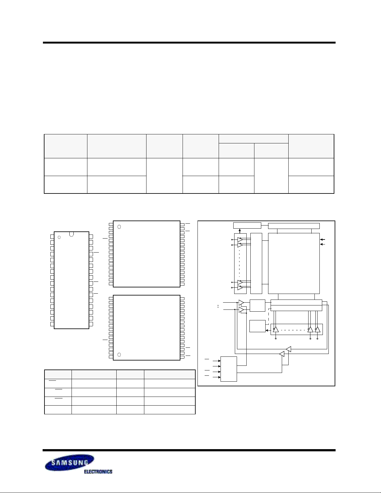
FEATURES
• Process Technology: TFT
• Organization: 128K x8
• Power Supply Voltage: 4.5~5.5V
• Low Data Retention Voltage: 2V(Min)
• Three state output and TTL Compatible
• Package Type: 32-DIP-600, 32-SOP-525,
32-TSOP1-0820F/R
PRODUCT FAMILY
Product Family Operating Temperature Vcc Range Speed
K6T1008C2C-L
K6T1008C2C-B
K6T1008C2C-P
Commercial(0~70°C)
55/70ns
4.5~5.5V
Industrial(-40~85°C) 70ns
K6T1008C2C-F
PIN DESCRIPTION
A11
1
A9
2
A8
3
A13
N.C
A16
A14
A12
I/O1
I/O2
I/O3
VSS
VCC
1
2
3
4
A7
5
6
A6
A5
7
8
9
10
11
12
13
14
15
16
32-DIP
32-SOP
A4
A3
A2
A1
A0
32
A15
31
CS2
30
WE
29
A13
28
A8
27
A9
26
25
A11
24
OE
23
A10
22
CS1
21
I/O8
20
I/O7
19
I/O6
18
I/O5
17
I/O4
CS2
A15
VCC
N.C
A16
A14
A12
A12
A14
A16
N.C
VCC
A15
CS2
A13
A11
4
WE
5
6
7
8
9
10
11
12
A7
13
A6
14
A5
15
A4
16
16
A4
15
A5
14
A6
13
A7
12
11
10
9
8
7
6
5
WE
4
3
A8
2
A9
1
32-TSOP
Type1 - Forward
32-TSOP
Type1 - Reverse
Name Function Name Function
CS1,CS2 Chip Select Inputs I/O1~I/O8 Data Inputs/Outputs
OE Output Enable Vcc Power
WE Write Enable Input Vss Ground
A0~A16 Address Inputs N.C No Connection
32
OE
A10
31
CS1
30
29
I/O8
I/O7
28
27
I/O6
26
I/O5
25
I/O4
24
VSS
23
I/O3
22
I/O2
21
I/O1
20
A0
19
A1
18
A2
17
A3
A3
17
A2
18
19
A1
20
A0
21
I/O1
22
I/O2
23
I/O3
24
VSS
25
I/O4
26
I/O5
27
I/O6
28
I/O7
29
I/O8
30
CS1
31
A10
32
OE
GENERAL DESCRIPTION
The K6T1008C2C families are fabricated by SAMSUNG′s
advanced CMOS process technology. The families support
various operating temperature ranges and have various
package types for user flexibility of system design. The families also support low data retention voltage for battery backup operation with low data retention current.
Power Dissipation
Standby
(ISB1, Max)
50µA
10µA
Operating
(ICC2, Max)
PKG Type
32-DIP, 32-SOP
32-TSOP1-F/R
60mA
50µA
15µA
32-SOP
32-TSOP1-F/R
FUNCTIONAL BLOCK DIAGRAM
CS1
CS2
WE
OE
I/O1
I/O8
A4
A5
A6
A7
A8
A12
A13
A14
A15
A16
Control
logic
Clk gen.
Row
select
Data
cont
Data
cont
Precharge circuit.
Memory array
1024 rows
128×8 columns
I/O Circuit
Column select
A0 A1 A2 A3 A9 A11A10
VCC
VSS
SAMSUNG ELECTRONICS CO., LTD. reserves the right to change products and specifications without notice.
2
Revision 2.0
November 1997
PRELIMINARY
K6T1008C2C Family CMOS SRAM
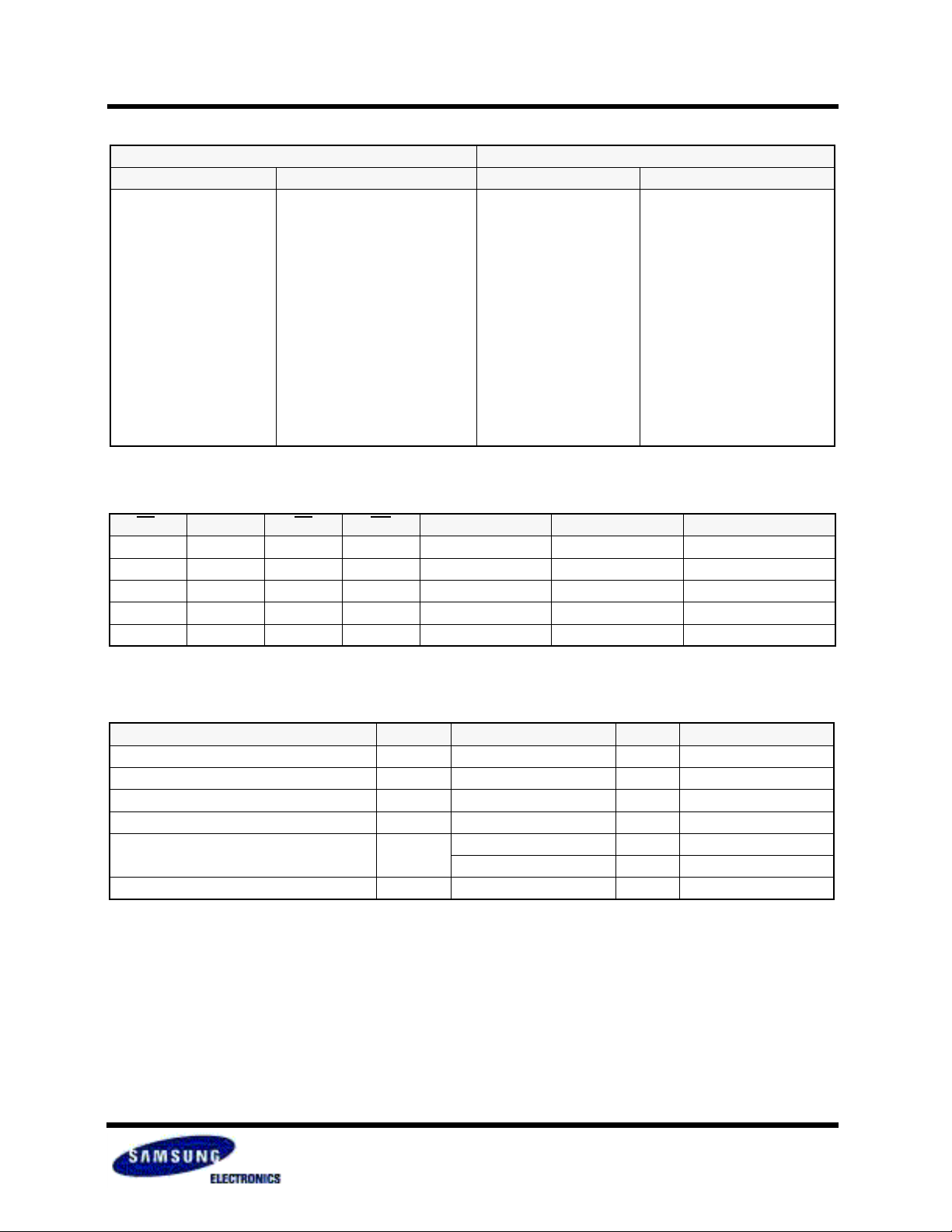
PRODUCT LIST
Commercial Temperature Products(0~70°C) Industrial Temperature Products(-40~85°C)
Part Name Function Part Name Function
K6T1008C2C-DL55
K6T1008C2C-DL70
K6T1008C2C-DB55
K6T1008C2C-DB70
K6T1008C2C-GL55
K6T1008C2C-GL70
K6T1008C2C-GB55
K6T1008C2C-GB70
K6T1008C2C-TB55
K6T1008C2C-TB70
32-DIP, 55ns, L-pwr
32-DIP, 70ns, L-pwr
32-DIP, 55ns, LL-pwr
32-DIP, 70ns, LL-pwr
32-SOP, 55ns, L-pwr
32-SOP, 70ns, L-pwr
32-SOP, 55ns, LL-pwr
32-SOP, 70ns, LL-pwr
32-TSOP1-F, 55ns, LL-pwr
32-TSOP1-F, 70ns, LL-pwr
K6T1008C2C-GP70
K6T1008C2C-GF70
K6T1008C2C-TF70
K6T1008C2C-RF70
32-SOP, 70ns, L-pwr
32-SOP, 70ns, LL-pwr
32-TSOP1-F, 70ns, LL-pwr
32-TSOP1-R, 70ns, LL-pwr
K6T1008C2C-RB55
K6T1008C2C-RB70
32-TSOP1-R, 55ns, LL-pwr
32-TSOP1-R, 70ns, LL-pwr
FUNCTIONAL DESCRIPTION
CS1 CS2 OE WE I/O Pin Mode Power
H
1)
X
1)
X
L
L H H H High-Z Output Disable Active
L H L H Dout Read Active
L H
1. X means don′t care(Must be in high or low status.)
ABSOLUTE MAXIMUM RATINGS
Item Symbol Ratings Unit Remark
Voltage on any pin relative to Vss VIN, VOUT -0.5 to 7.0 V Voltage on Vcc supply relative to Vss VCC -0.5 to 7.0 V Power Dissipation PD 1.0 W Storage temperature TSTG -65 to 150 °C -
Operating Temperature TA
Soldering temperature and time TSOLDER 260°C, 10sec (Lead Only) - -
1. Stresses greater than those listed under "Absolute Maximum Ratings" may cause permanent damage to the device. Functional operation should be
restricted to recommended operating condition. Exposure to absolute maximum rating conditions for extended periods may affect reliability.
1)
X
1)
X
1)
X
1)
X
1)
X
High-Z Deselected Standby
High-Z Deselected Standby
L Din Write Active
1)
0 to 70 °C K6T1008C2C-L
-40 to 85 °C K6T1008C2C-P
3
Revision 2.0
November 1997
 Loading...