

SAMSUNG K6E0808C1E-C Technical data

K6E0808C1E-C/E-L, K6E0808C1E-I/E-P
Document Title
32Kx8 Bit High-Speed CMOS Static RAM(5V Operating).
Operated at Commercial and Industrial Temperature Ranges.
Revision History
For Cisco
CMOS SRAM
Rev .No.
Rev. 0.0
Rev. 1.0
Rev. 2.0
History
Initial release with Preliminary.
Release to Final Data Sheet.
2.1. Add Low Power Version.
2.2. Add data retention charactoristic.
Draft Data
Aug. 1. 1998
Nov. 2. 1998
Feb. 25. 1999
Remark
Preliminary
Final
Final
The attached data sheets are prepared and approved by SAMSUNG Electronics. SAMSUNG Electronics CO., LTD. reserve the right to change the
specifications. SAMSUNG Electronics will evaluate and reply to your requests and questions on the parameters of this device. If you have any questions, please contact the SAMSUNG branch office near your office, call or contact Headquarters.
- 1 -
Revision 2.0
Feburary 1999
K6E0808C1E-C/E-L, K6E0808C1E-I/E-P
32K x 8 Bit High-Speed CMOS Static RAM
GENERAL DESCRIPTIONFEATURES
• Fast Access Time 10, 12, 15ns(Max.)
• Low Power Dissipation
Standby (TTL) : 20mA(Max.)
(CMOS) : 2mA(Max.)
0.6mA(Max.) L-ver. Only
Operating K6E0808C1E-10 : 80mA(Max.)
K6E0808C1E-12 : 80mA(Max.)
K6E0808C1E-15 : 80mA(Max.)
• Single 5.0V±10% Power Supply
• TTL Compatible Inputs and Outputs
• I/O Compatible with 3.3V Device
• Fully Static Operation
- No Clock or Refresh required
• Three State Outputs
• 2V Minimum Data Retention : L-Ver. only
• Standard Pin Configuration
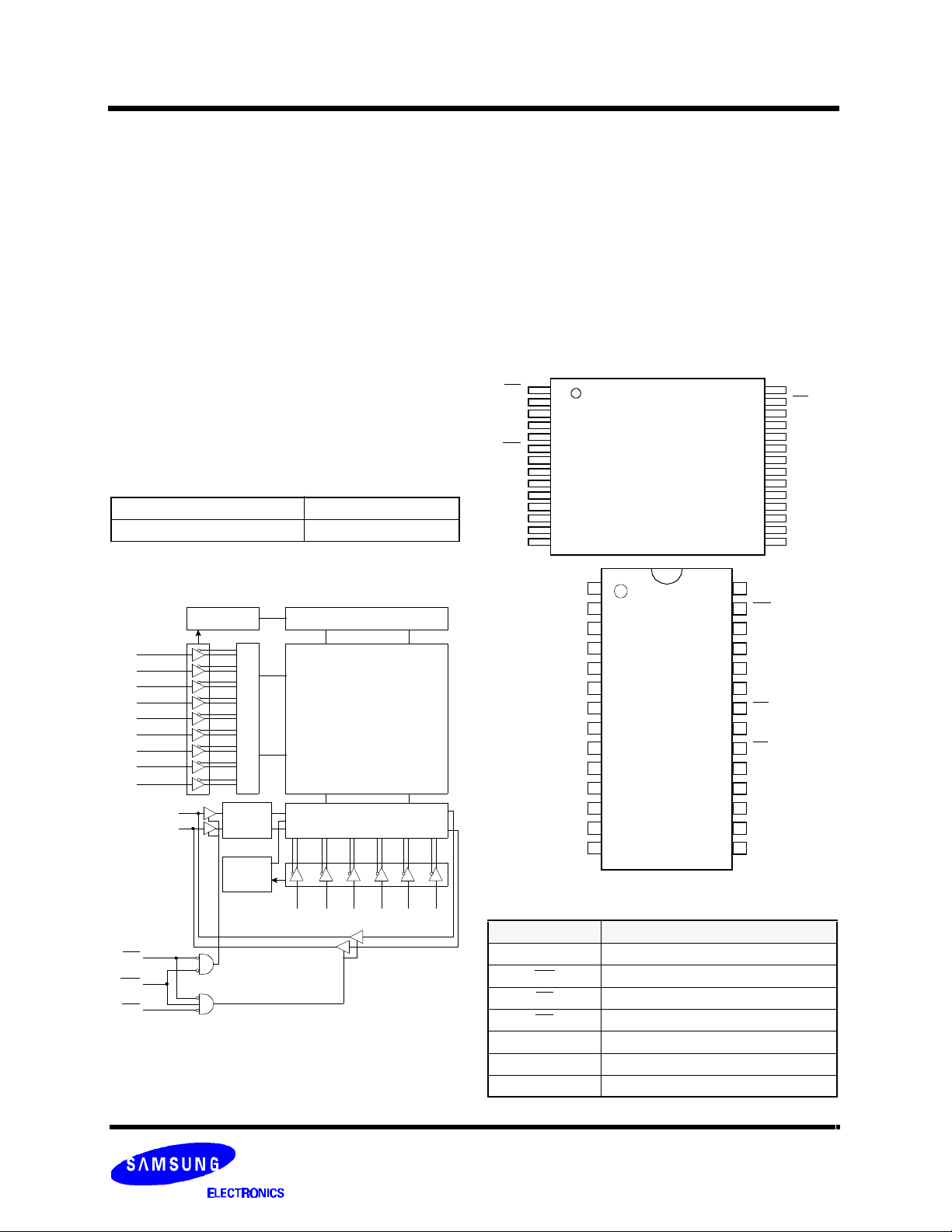
K6E0808C1E-J : 28-SOJ-300
K6E0808C1E-T : 28-TSOP1-0813. 4F
ORDERING INFORMATION
K6E0808C1E-C10/C12/C15 Commercial Temp.
K6E0808C1E-I10/I12/I15 Industrial Temp.
The K6E0808C1E is a 262,144-bit high-speed Static Random
Access Memory organized as 32,768 words by 8 bits. The
K6E0808C1E uses 8 common input and output lines and has
an output enable pin which operates faster than address access
time at read cycle. The device is fabricated using SAMSUNG′s
advanced CMOS process and designed for high-speed circuit
technology. It is particularly well suited for use in high-density
high-speed system applications. The K6E0808C1E is packaged
in a 300mil 28-pin plastic SOJ or TSOP1 forward.
OE
A11
A9
A8
A13
WE
Vcc
A14
A12
A7
A6
A5
A4
A3
For Cisco
CMOS SRAM
PIN CONFIGURATION(Top View)
1
2
3
4
5
6
7
8
9
10
11
12
13
14
TSOP1
28
27
26
25
24
23
22
21
20
19
18
17
16
15
A10
CS
I/O8
I/O7
I/O6
I/O5
I/O4
Vss
I/O3
I/O2
I/O1
A0
A1
A2
FUNCTIONAL BLOCK DIAGRAM
A0
A1
A2
A3
A4
A5
A6
A7
A8
CS
WE
OE
I/O1~I/O8
Clk Gen.
Row Select
Data
Cont.
CLK
Gen.
Pre-Charge-Circuit
Memory Array
512 Rows
64x8 Columns
I/O Circuit
Column Select
A9 A10 A11 A12 A13 A14
1
A14
2
A12
3
A7
4
A6
5
A5
6
A4
7
I/O1
I/O2
I/O3
Vss
A3
8
A2
9
A1
10
A0
11
12
13
14
SOJ
PIN FUNCTION
Pin Name Pin Function
A0 - A14 Address Inputs
WE Write Enable
CS Chip Select
OE Output Enable
I/O1 ~ I/O8 Data Inputs/Outputs
VCC Power(+5.0V)
VSS Ground
28
Vcc
27
WE
26
A13
25
A8
24
A9
23
A11
22
OE
21
A10
20
CS
19
I/O8
18
I/O7
17
I/O6
16
I/O5
15
I/O4
- 2 -
Revision 2.0
Feburary 1999
For Cisco
K6E0808C1E-C/E-L, K6E0808C1E-I/E-P
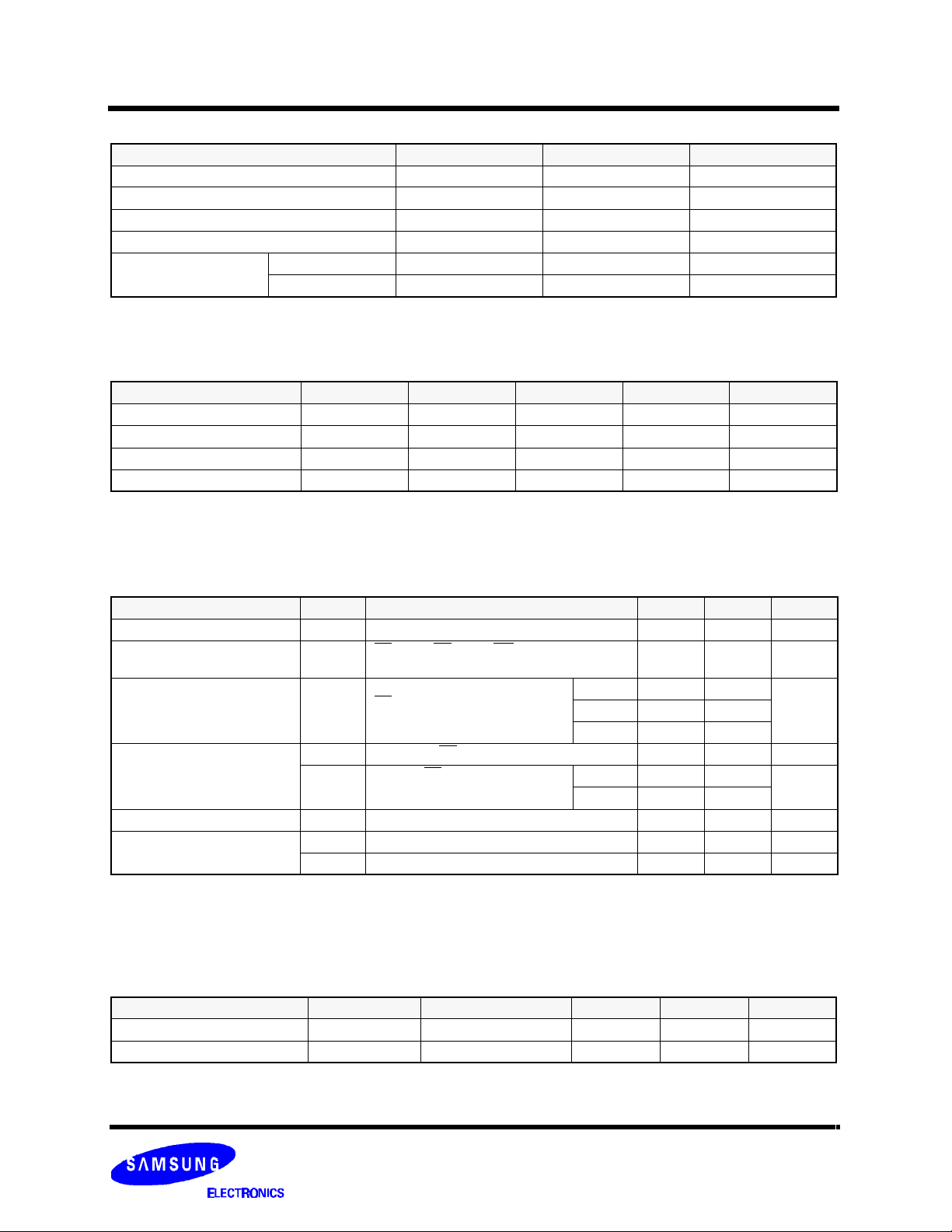
ABSOLUTE MAXIMUM RATINGS*
Parameter Symbol Rating Unit
Voltage on Any Pin Relative to VSS VIN, VOUT -0.5 to 7.0 V
Voltage on VCC Supply Relative to VSS VCC -0.5 to 7.0 V
Power Dissipation PD 1.0 W
Storage Temperature TSTG -65 to 150 °C
Operating Temperature Commercial TA 0 to 70 °C
Industrial TA -40 to 85 °C
* Stresses greater than those listed under "Absolute Maximum Ratings" may cause permanent damage to the device. This is a stress rating only and
functional operation of the device at these or any other conditions above those indicated in the operating sections of this specification is not implied.
Exposure to absolute maximum rating conditions for extended periods may affect reliability.
RECOMMENDED DC OPERATING CONDITIONS*(TA=0 to 70°C)
Parameter Symbol Min Typ Max Unit
Supply Voltage VCC 4.5 5.0 5.5 V
Ground VSS 0 0 0 V
Input High Voltage VIH 2.2 - VCC+0.5***
Input Low Voltage VIL -0.5** - 0.8
* The above parameters are also guaranteed at industrial temperature range.
** VIL(Min) = -2.0(Pulse Width≤7ns) for I≤20mA.
*** VIH(Max) = VCC+2.0V(Pulse Width≤7ns) for I≤20mA.
CMOS SRAM
V
V
DC AND OPERATING CHARACTERISTICS*(TA=0 to 70°C,VCC=5.0V±10% unless otherwise specified)
Parameter Symbol Test Conditions
Input Leakage Current ILI VIN = VSS to VCC -2 2 µA
Output Leakage Current ILO CS=VIH or OE=VIH or WE=VIL
Operating Current ICC Min. Cycle, 100% Duty
Standby Current ISB Min. Cycle, CS=VIH - 20 mA
ISB1 f=0MHz, CS≥VCC-0.2V,
Output Low Voltage Level VOL IOL=8mA - 0.4 V
Output High Voltage Level VOH IOH=-4mA 2.4 - V
VOH1** IOH1=0.1mA - 3.95 V
* The above parameters are also guaranteed at industrial temperature range.
** VCC=5.0V±5%, Temp.=25°C.
VOUT = VSS to VCC
CS=VIL, VIN = VIH or VIL,
IOUT=0mA
VIN≥VCC-0.2V or VIN≤0.2V
10ns - 80 mA
12ns - 80
15ns - 80
Normal - 2 mA
L-Ver - 0.6
Min Max
-2 2 µA
Unit
CAPACITANCE*(TA=25°C, f=1.0MHz)
Item Symbol Test Conditions MIN Max Unit
Input/Output Capacitance CI/O VI/O=0V - 8 pF
Input Capacitance CIN
* Capacitance is sampled and not 100% tested.
VIN=0V
- 7 pF
- 3 -
Revision 2.0
Feburary 1999
 Loading...