SAMSUNG K5T6432YTBM Technical data

现货库存、技术资料、百科信息、热点资讯,精彩尽在鼎好!
Document Title
Multi-Chip Package MEMORY
64M Bit (4Mx16) Four Bank NOR Flash Memory / 32M Bit (2Mx16) UtRAM
Revision History
MCP MEMORYK5T6432YT(B)M
Revision No.
1.0
History
Final Specification
Draft Date
November 27, 2001
Remark
Final
The attached datasheets are provided by SAMSUNG Electronics. SAMSUNG Electronics CO., LTD. reserve the right to change the specifications and
products. SAMSUNG Electronics will answer to your questions about device. If you have any questions, please contact the SAMSUNG branch offices.
- 1 -
Revision 1.0
November 2001
Multi-Chip Package MEMORY
64M Bit (4Mx16) Four Bank NOR Flash Memory / 32M Bit (2Mx16) UtRAM
MCP MEMORYK5T6432YT(B)M
FEATURES
• Power Supply voltage : 2.7 to 3.3 V
• Organization
- Flash : 4,194,304 x 16 bit
- UtRAM : 2,097,152 x 16 bit
• Access Time (@2.7V)
- Flash : 85 ns, UtRAM : 100 ns
• Power Consumption (typical value)
- Flash Read Current : 20 mA (@5MHz)
Sequential Page Read Current : 5 mA (@5MHz)
Program/Erase Current : 35 mA (Max.)
Standby mode/Deep Power mode : 0.1 µA
- UtRAM Operating Current : 18 mA
Standby Current :120 µA
Deep Power Down : 5 µA
• Secode(Security Code) Block : Extra 32KW Block (Flash)
• Block Group Protection / Unprotection (Flash)
• 128 words Page Program (Flash)
• Flash Bank Size : 4Mb / 4Mb / 28Mb / 28Mb
• Flash Endurance : 100,000 Program/Erase Cycles
GENERAL DESCRIPTION
The K5T6432YT(B)M featuring single 3.0V power supply is a
Multi Chip Package Memory which combines 64Mbit Four Bank
Flash and 32Mbit UtRAM.
The 64Mbit Flash memory is organized as 4M x16 bit and 32Mbit
UtRAM is organized as 2M x16 bit. The 64Mbit Flash memory is
the high performance non-volatile memory fabricated by CMOS
technology for peripheral circuit and DINOR IV(Diveded bit-line
NOR IV) architecture for the memory cell. All memory blocks are
locked and can be programmed or erased, when F-WP is low.
Using Software Lock Release function, program erase operation
can be executed.
The 32Mbit UtRAM is fabricated by SAMSUNG’s advanced
CMOS technology using one transistor memory cell.
The device also supports deep power down mode for low standby
current. The K5T6432YT(B)M is suitable for use in program and
data memory of mobile communication system to reduce mount
area. This device is available in 81-ball TBGA Type package.
• Ambient Temperature : -25°C ~ 85°C
• Endurance : 100,000 Program/Erase Cycles
• Package :81 - ball TBGA Type - 10.8 x 10.4 mm, 0.8 mm pitch
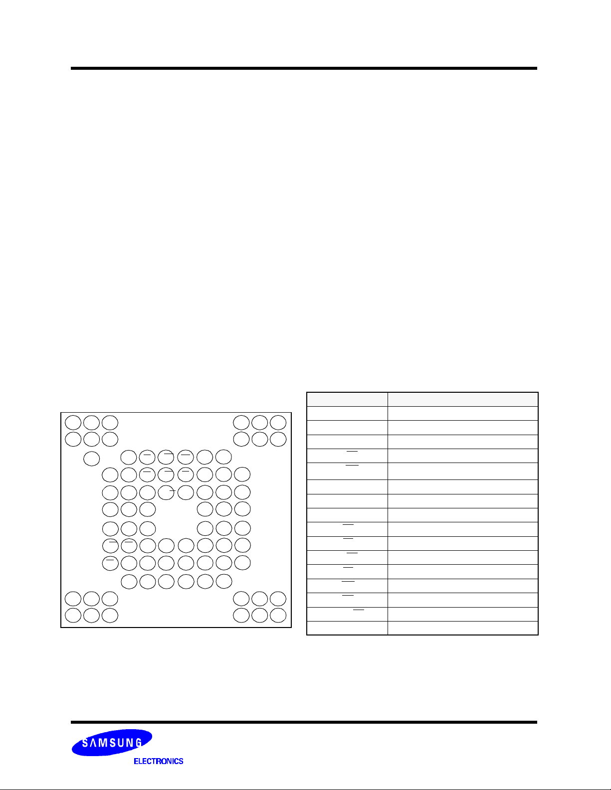
BALL CONFIGURATION BALL DESCRIPTION
1
N.C
N.C
N
A16
F-Vcc
Vss
N.C
N.C
1
.
C
1
N.CN.
N.CN.
N.CN.
N.CN.
1
2
C
C
C
C
7
8
A
8
A19
A10
DQ6
1
12DQ7
DQ5
DQ1
3
DQ1
910
A11
12A15
A
A13A2
A14
N.C
5
4
5
2
3
1
N.CN.
N.C
A
N.C
B
C
N.C
N.C
D
E
F
G
H
J
K
L
N.C
N.CN.
N.CN.
N.C
M
4
C
N.C
A
7
A3A
6
A2A5A18
A
1
A
4
V
S
S
A
0
F-CEO
E
DQ0DQ10
C
S
DQ8DQ2D
C
C
6
F-W
P
L
B
U
B
A17
DQ1
DQ9DQ3DQ4DQ
F-R
F
-RY/B
F-Vcc
Q
P
Y
1
1
W
E
Z
Z
A20A9
VccDQ
N.C
Ball Name Description
A0 to A20 Address Input Balls (Common)
A21 Address Input Ball (Flash Memory)
DQ0 to DQ15 Data Input/Output Balls (Common)
F-RP Hardware Reset (Flash Memory)
F-WP Write Protect (Flash Memory)
F-Vcc Power Supply (Flash Memory)
Vcc Power Supply (UtRAM))
Vss Ground (Common)
UB Upper Byte Enable (UtRAM)
LB Lower Byte Enable (UtRAM)
F-CE Chip Enable (Flash Memory)
ZZ Deep Power Down (UtRAM)
WE Write Enable (Common)
OE Output Enable (Common)
F-RY/BY Ready/Busy (Flash memory)
N.C No Connection
81 Ball TBGA , 0.8mm Pitch
Top View (Ball Down)
SAMSUNG ELECTRONICS CO., LTD. reserves the right to change products and specifications without notice.
- 2 -
November 2001
Revision 1.0
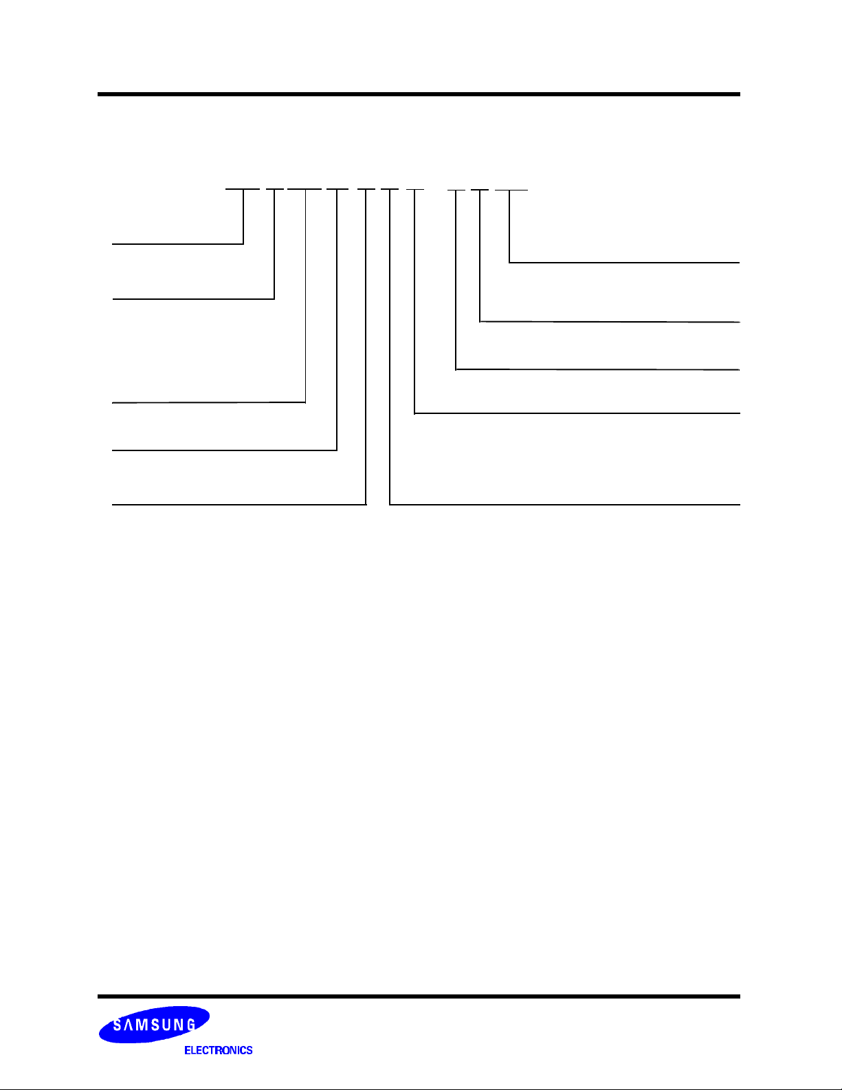
ORDERING INFORMATION
K 5 T 64 32 Y T M - T 3 10
Samsung
MCP Memory
Device Type
Mitsubishi NOR Flash
+ UtRAM
MCP MEMORYK5T6432YT(B)M
UtRAM Access Time
10 = 100 ns
Flash Access Time
3 = 85 ns
NOR Flash Density
(Organization) , (BankSize)
64 : 64Mbit (x16 Selectable)
(4Mb, 4Mb, 28Mb,2 8Mb)
UtRAM Density , Organization
32Mbit , x16 Selectable
Operating Voltage Range
2.7V to 3.3V
Package
T = 81 TBGA
Version
M = 1st Generation
Block Architecture
T = Top Boot Block
B = Bottom Boot Block
- 3 -
Revision 1.0
November 2001
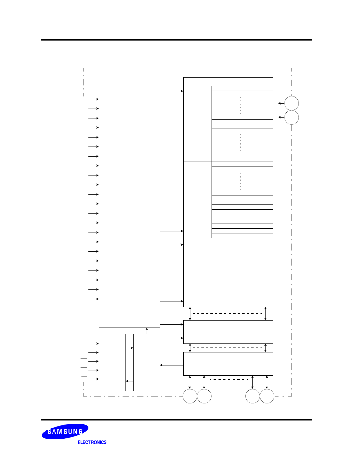
Flash Memory Part
MCP MEMORYK5T6432YT(B)M
128-word Page Buffer
Main Block 134 32K-word
Address
Input
A21
A20
A19
A18
A17
A16
A15
A14
A13
A12
A11
A10
A9
A8
A7
A6
A5
A4
A3
A2
A1
A0
X-decorder
Y-Decorder
Bank4
56 blocks
Bank3
56 blocks
Bank2
8 blocks
Bank1
15 blocks
Main Block 79 32K-word
Main Block 78 32K-word
Main Block 23 32K-word
Main Block 22 32K-word
Main Block 15 32K-word
Main Block 14 32K-word
Main Block 8 32K-word
Parameter Block 7 4K-word
Parameter Block 2 4K-word
Boot Block 1 4K-word
Bppt Block 0 4K-word
Y-Gate / Sense Amp.
F-Vcc
Vss
Chip Enable
Output Enable
Write Enable
Write Protect
Reset
/PowerDown
Status/ ID Register
Multi Plexer
F-CE
OE
WE
F-WP
F-RP
Command
User
Interface
Write
State
Machine
I/O Buffer
DQ15 DQ14 DQ1 DQ0
Data I/O
FUNCTIONAL BLOCK DIAGRAM (64Mbit Flash Memory)
- 4 -
Revision 1.0
November 2001

Table 1. Flash Memory Top Boot Block Address (K5T6432YT)
K5T6432YT Block Block Size
BA134 4 Kwords 3FF000H-3FFFFFH
BA133 4 Kwords 3FE000H-3FEFFFH
BA132 4 Kwords 3FD000H-3FDFFFH
BA131 4 Kwords 3FC000H-3FCFFFH
BA130 4 Kwords 3FB000H-3FBFFFH
BA129 4 Kwords 3FA000H-3FAFFFH
Bank4
Bank3
Bank2
BA128 4 Kwords 3F9000H-3F9FFFH
BA127 4 Kwords 3F8000H-3F8FFFH
BA126 32 Kwords 3F0000H-3F7FFFH
BA125 32 Kwords 3E8000H-3EFFFFH
BA124 32 Kwords 3E0000H-3E7FFFH
BA123 32 Kwords 3D8000H-3DFFFFH
BA122 32 Kwords 3D0000H-3D7FFFH
BA121 32 Kwords 3C8000H-3CFFFFH
BA120 32 Kwords 3C0000H-3C7FFFH
BA119 32 Kwords 3B8000H-3BFFFFH
BA118 32 Kwords 3B0000H-3B7FFFH
BA117 32 Kwords 3A8000H-3AFFFFH
BA116 32 Kwords 3A0000H-3A7FFFH
BA115 32 Kwords 398000H-39FFFFH
BA114 32 Kwords 390000H-397FFFH
BA113 32 Kwords 388000H-38FFFFH
BA112 32 Kwords 380000H-387FFFH
BA111 32 Kwords 378000H-37FFFFH
BA110 32 Kwords 370000H-377FFFH
BA109 32 Kwords 368000H-36FFFFH
BA108 32 Kwords 360000H-367FFFH
BA107 32 Kwords 358000H-35FFFFH
BA106 32 Kwords 350000H-357FFFH
BA105 32 Kwords 348000H-34FFFFH
BA104 32 Kwords 340000H-347FFFH
BA103 32 Kwords 338000H-33FFFFH
BA102 32 Kwords 330000H-337FFFH
BA101 32 Kwords 328000H-32FFFFH
BA100 32 Kwords 320000H-327FFFH
BA99 32 Kwords 318000H-31FFFFH
BA98 32 Kwords 310000H-317FFFH
BA97 32 Kwords 208000H-20FFFFH
BA96 32 Kwords 300000H-307FFFH
BA95 32 Kwords 2F8000H-2FFFFFH
BA94 32 Kwords 2F0000H-2F7FFFH
BA93 32 Kwords 2E8000H-2EFFFFH
BA92 32 Kwords 2E0000H-2E7FFFH
BA91 32 Kwords 2D8000H-2DFFFFH
BA90 32 Kwords 2D0000H-2D7FFFH
MCP MEMORYK5T6432YT(B)M
Address Range
Word Mode (x16)
- 5 -
Revision 1.0
November 2001

Table 1. Flash Memory Top Boot Block Address (K5T6432YT)
K5T6432YT Block Block Size
BA89 32 Kwords 2C8000H-2CFFFFH
BA88 32 Kwords 2C0000H-2C7FFFH
BA87 32 Kwords 2B8000H-2BFFFFH
BA86 32 Kwords 2B0000H-2B7FFFH
BA85 32 Kwords 2A8000H-2AFFFFH
BA84 32 Kwords 2A0000H-2A7FFFH
BA83 32 Kwords 298000H-29FFFFH
BA82 32 Kwords 290000H-297FFFH
BA81 32 Kwords 288000H-28FFFFH
BA80 32 Kwords 280000H-287FFFH
BA79 32 Kwords 278000H-27FFFFH
BA78 32 Kwords 270000H-277FFFH
BA77 32 Kwords 268000H-26FFFFH
Bank2
Bank1
BA76 32 Kwords 260000H-267FFFH
BA75 32 Kwords 258000H-25FFFFH
BA74 32 Kwords 250000H-257FFFH
BA73 32 Kwords 248000H-24FFFFH
BA72 32 Kwords 240000H-247FFFH
BA71 32 Kwords 238000H-23FFFFH
BA70 32 Kwords 230000H-237FFFH
BA69 32 Kwords 228000H-22FFFFH
BA68 32 Kwords 220000H-227FFFH
BA67 32 Kwords 218000H-21FFFFH
BA66 32 Kwords 210000H-217FFFH
BA65 32 Kwords 208000H-20FFFFH
BA64 32 Kwords 200000H-207FFFH
BA63 32 Kwords 1F8000H-1FFFFFH
BA62 32 Kwords 1F0000H-1F7FFFH
BA61 32 Kwords 1E8000H-1EFFFFH
BA60 32 Kwords 1E0000H-1E7FFFH
BA59 32 Kwords 1D8000H-1DFFFFH
BA58 32 Kwords 1D0000H-1D7FFFH
BA57 32 Kwords 1C8000H-1CFFFFH
BA56 32 Kwords 1C0000H-1C7FFFH
BA55 32 Kwords 1B8000H-1BFFFFH
BA54 32 Kwords 1B0000H-1B7FFFH
BA53 32 Kwords 1A8000H-1AFFFFH
BA52 32 Kwords 1A0000H-1A7FFFH
BA51 32 Kwords 198000H-19FFFFH
BA50 32 Kwords 190000H-197FFFH
BA49 32 Kwords 188000H-18FFFFH
BA48 32 Kwords 180000H-187FFFH
BA47 32 Kwords 178000H-17FFFFH
BA46 32 Kwords 170000H-177FFFH
BA45 32 Kwords 168000H-16FFFFH
MCP MEMORYK5T6432YT(B)M
Address Range
Word Mode (x16)
- 6 -
Revision 1.0
November 2001

Table 1. Flash Memory Top Boot Block Address (K5T6432YT)
K5T6432YT Block Block Size
BA44 32 Kwords 160000H-167FFFH
BA43 32 Kwords 158000H-15FFFFH
BA42 32 Kwords 150000H-157FFFH
BA41 32 Kwords 148000H-14FFFFH
BA40 32 Kwords 140000H-147FFFH
BA39 32 Kwords 138000H-13FFFFH
BA38 32 Kwords 130000H-137FFFH
BA37 32 Kwords 128000H-12FFFFH
BA36 32 Kwords 120000H-127FFFH
BA35 32 Kwords 118000H-11FFFFH
BA34 32 Kwords 110000H-117FFFH
BA33 32 Kwords 108000H-10FFFFH
BA32 32 Kwords 100000H-107FFFH
BA31 32 Kwords F8000H-FFFFFH
BA30 32 Kwords F0000H-F7FFFH
BA29 32 Kwords E8000H-EFFFFH
BA28 32 Kwords E0000H-E7FFFH
BA27 32 Kwords D8000H-DFFFFH
Bank1
BA26 32 Kwords D0000H-D7FFFH
BA25 32 Kwords C8000H-CFFFFH
BA24 32 Kwords C0000H-C7FFFH
BA23 32 Kwords B8000H-BFFFFH
BA22 32 Kwords B0000H-B7FFFH
BA21 32 Kwords A8000H-AFFFFH
BA20 32 Kwords A0000H-A7FFFH
BA19 32 Kwords 98000H-9FFFFH
BA18 32 Kwords 90000H-97FFFH
BA17 32 Kwords 88000H-8FFFFH
BA16 32 Kwords 80000H-87FFFH
BA15 32 Kwords 78000H-7FFFFH
BA14 32 Kwords 70000H-77FFFH
BA13 32 Kwords 68000H-6FFFFH
BA12 32 Kwords 60000H-67FFFH
BA11 32 Kwords 58000H-5FFFFH
BA10 32 Kwords 50000H-57FFFH
BA9 32 Kwords 48000H-4FFFFH
BA8 32 Kwords 40000H-47FFFH
BA7 32 Kwords 38000H-3FFFFH
BA6 32 Kwords 30000H-37FFFH
BA5 32 Kwords 28000H-2FFFFH
BA4 32 Kwords 20000H-27FFFH
BA3 32 Kwords 18000H-1FFFFH
BA2 32 Kwords 10000H-17FFFH
BA1 32 Kwords 08000H-0FFFFH
BA0 32 Kwords 00000H-07FFFH
MCP MEMORYK5T6432YT(B)M
Address Range
Word Mode (x16)
- 7 -
Revision 1.0
November 2001

Table 2. Flash Memory Bottom Boot Block Address (K5T6432YB)
K5T6432YB Block Block Size
BA134 32 Kwords 3F8000H-3FFFFFH
BA133 32 Kwords 3F0000H-3F7FFFH
BA132 32 Kwords 3E8000H-3EFFFFH
BA131 32 Kwords 3E0000H-3E7FFFH
BA130 32 Kwords 3D8000H-3DFFFFH
BA129 32 Kwords 3D0000H-3D7FFFH
BA128 32 Kwords 3C8000H-3CFFFFH
BA127 32 Kwords 3C0000H-3C7FFFH
BA126 32 Kwords 3B8000H-3BFFFFH
BA125 32 Kwords 3B0000H-3B7FFFH
BA124 32 Kwords 3A8000H-3AFFFFH
BA123 32 Kwords 3A0000H-3A7FFFH
BA122 32 Kwords 398000H-39FFFFH
BA121 32 Kwords 390000H-397FFFH
BA120 32 Kwords 388000H-38FFFFH
BA119 32 Kwords 380000H-387FFFH
BA118 32 Kwords 378000H-37FFFFH
BA117 32 Kwords 370000H-377FFFH
BA116 32 Kwords 368000H-36FFFFH
BA115 32 Kwords 360000H-367FFFH
BA114 32 Kwords 358000H-35FFFFH
Bank4
BA113 32 Kwords 350000H-357FFFH
BA112 32 Kwords 348000H-34FFFFH
BA111 32 Kwords 340000H-347FFFH
BA110 32 Kwords 338000H-33FFFFH
BA109 32 Kwords 330000H-337FFFH
BA108 32 Kwords 328000H-32FFFFH
BA107 32 Kwords 320000H-327FFFH
BA106 32 Kwords 318000H-31FFFFH
BA105 32 Kwords 310000H-317FFFH
BA104 32 Kwords 208000H-20FFFFH
BA103 32 Kwords 300000H-307FFFH
BA102 32 Kwords 2F8000H-2FFFFFH
BA101 32 Kwords 2F0000H-2F7FFFH
BA100 32 Kwords 2E8000H-2EFFFFH
BA99 32 Kwords 2E0000H-2E7FFFH
BA98 32 Kwords 2D8000H-2DFFFFH
BA97 32 Kwords 2D0000H-2D7FFFH
BA96 32 Kwords 2C8000H-2CFFFFH
BA95 32 Kwords 2C0000H-2C7FFFH
BA94 32 Kwords 2B8000H-2BFFFFH
BA93 32 Kwords 2B0000H-2B7FFFH
BA92 32 Kwords 2A8000H-2AFFFFH
BA91 32 Kwords 2A0000H-2A7FFFH
BA90 32 Kwords 298000H-29FFFFH
MCP MEMORYK5T6432YT(B)M
Address Range
Word Mode (x16)
- 8 -
Revision 1.0
November 2001

Table 2. Flash Memory Bottom Boot Block Address (K5T6432YB)
K5T6432YB Block Block Size
BA89 32 Kwords 290000H-297FFFH
BA88 32 Kwords 288000H-28FFFFH
BA87 32 Kwords 280000H-287FFFH
BA86 32 Kwords 278000H-27FFFFH
Bank4
Bank3
BA85 32 Kwords 270000H-277FFFH
BA84 32 Kwords 268000H-26FFFFH
BA83 32 Kwords 260000H-267FFFH
BA82 32 Kwords 258000H-25FFFFH
BA81 32 Kwords 250000H-257FFFH
BA80 32 Kwords 248000H-24FFFFH
BA79 32 Kwords 240000H-247FFFH
BA78 32 Kwords 238000H-23FFFFH
BA77 32 Kwords 230000H-237FFFH
BA76 32 Kwords 228000H-22FFFFH
BA75 32 Kwords 220000H-227FFFH
BA74 32 Kwords 218000H-21FFFFH
BA73 32 Kwords 210000H-217FFFH
BA72 32 Kwords 208000H-20FFFFH
BA71 32 Kwords 200000H-207FFFH
BA70 32 Kwords 1F8000H-1FFFFFH
BA69 32 Kwords 1F0000H-1F7FFFH
BA68 32 Kwords 1E8000H-1EFFFFH
BA67 32 Kwords 1E0000H-1E7FFFH
BA66 32 Kwords 1D8000H-1DFFFFH
BA65 32 Kwords 1D0000H-1D7FFFH
BA64 32 Kwords 1C8000H-1CFFFFH
BA63 32 Kwords 1C0000H-1C7FFFH
BA62 32 Kwords 1B8000H-1BFFFFH
BA61 32 Kwords 1B0000H-1B7FFFH
BA60 32 Kwords 1A8000H-1AFFFFH
BA59 32 Kwords 1A0000H-1A7FFFH
BA58 32 Kwords 198000H-19FFFFH
BA57 32 Kwords 190000H-197FFFH
BA56 32 Kwords 188000H-18FFFFH
BA55 32 Kwords 180000H-187FFFH
BA54 32 Kwords 178000H-17FFFFH
BA53 32 Kwords 170000H-177FFFH
BA52 32 Kwords 168000H-16FFFFH
BA51 32 Kwords 160000H-167FFFH
BA50 32 Kwords 158000H-15FFFFH
BA49 32 Kwords 150000H-157FFFH
BA48 32 Kwords 148000H-14FFFFH
BA47 32 Kwords 140000H-147FFFH
BA46 32 Kwords 138000H-13FFFFH
BA45 32 Kwords 130000H-137FFFH
MCP MEMORYK5T6432YT(B)M
Address Range
Word Mode (x16)
- 9 -
Revision 1.0
November 2001
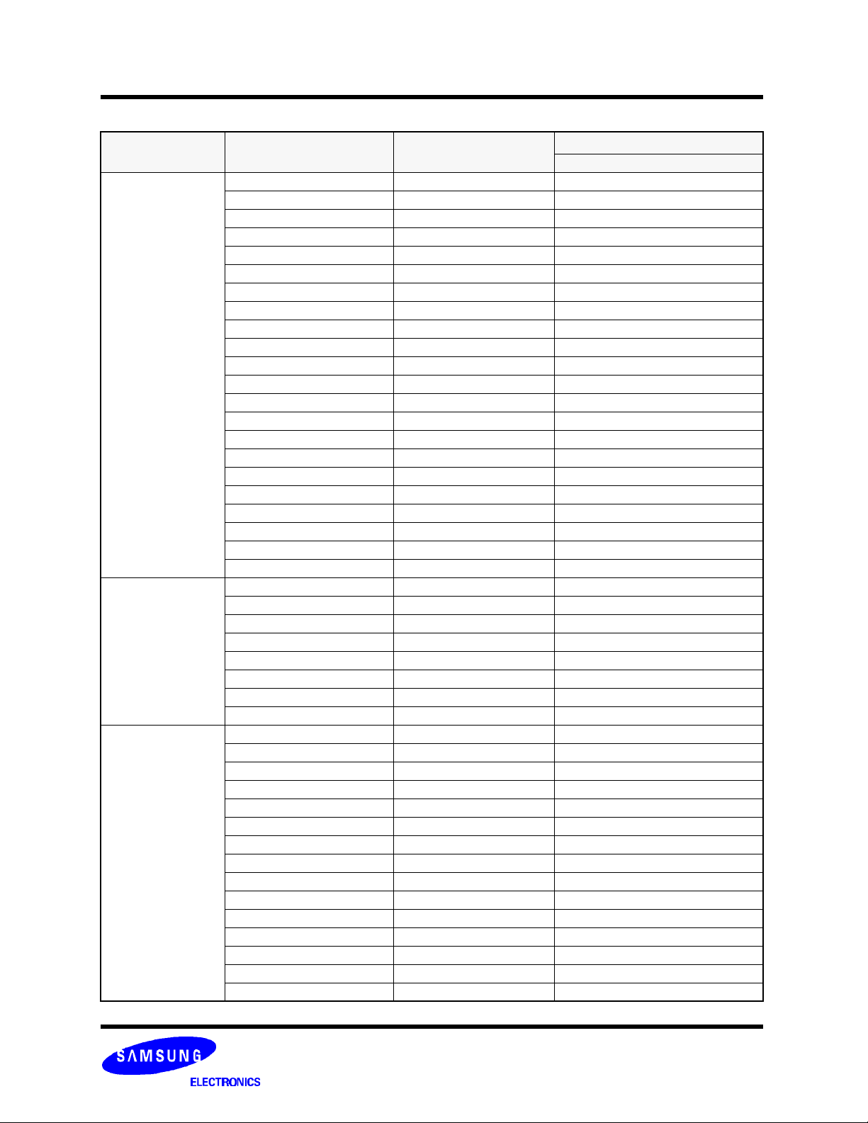
Table 2. Flash Memory Bottom Boot Block Address (K5T6432YB)
K5T6432YB Block Block Size
BA44 32 Kwords 128000H-12FFFFH
BA43 32 Kwords 120000H-127FFFH
BA42 32 Kwords 118000H-11FFFFH
BA41 32 Kwords 110000H-117FFFH
BA40 32 Kwords 108000H-10FFFFH
BA39 32 Kwords 100000H-107FFFH
BA38 32 Kwords F8000H-FFFFFH
BA37 32 Kwords F0000H-F7FFFH
BA36 32 Kwords E8000H-EFFFFH
Bank3
Bank2
Bank1
BA35 32 Kwords E0000H-E7FFFH
BA34 32 Kwords D8000H-DFFFFH
BA33 32 Kwords D0000H-D7FFFH
BA32 32 Kwords C8000H-CFFFFH
BA31 32 Kwords C0000H-C7FFFH
BA30 32 Kwords B8000H-BFFFFH
BA29 32 Kwords B0000H-B7FFFH
BA28 32 Kwords A8000H-AFFFFH
BA27 32 Kwords A0000H-A7FFFH
BA26 32 Kwords 98000H-9FFFFH
BA25 32 Kwords 90000H-97FFFH
BA24 32 Kwords 88000H-8FFFFH
BA23 32 Kwords 80000H-87FFFH
BA22 32 Kwords 78000H-7FFFFH
BA21 32 Kwords 70000H-77FFFH
BA20 32 Kwords 68000H-6FFFFH
BA19 32 Kwords 60000H-67FFFH
BA18 32 Kwords 58000H-5FFFFH
BA17 32 Kwords 50000H-57FFFH
BA16 32 Kwords 48000H-4FFFFH
BA15 32 Kwords 40000H-47FFFH
BA14 32 Kwords 38000H-3FFFFH
BA13 32 Kwords 30000H-37FFFH
BA12 32 Kwords 28000H-2FFFFH
BA11 32 Kwords 20000H-27FFFH
BA10 32 Kwords 18000H-1FFFFH
BA9 32 Kwords 10000H-17FFFH
BA8 32 Kwords 08000H-0FFFFH
BA7 4 Kwords 07000H-07FFFH
BA6 4 Kwords 06000H-06FFFH
BA5 4 Kwords 05000H-05FFFH
BA4 4 Kwords 04000H-04FFFH
BA3 4 Kwords 03000H-03FFFH
BA2 4 Kwords 02000H-02FFFH
BA1 4 Kwords 01000H-01FFFH
BA0 4 Kwords 00000H-00FFFH
MCP MEMORYK5T6432YT(B)M
Address Range
Word Mode (x16)
- 10 -
Revision 1.0
November 2001
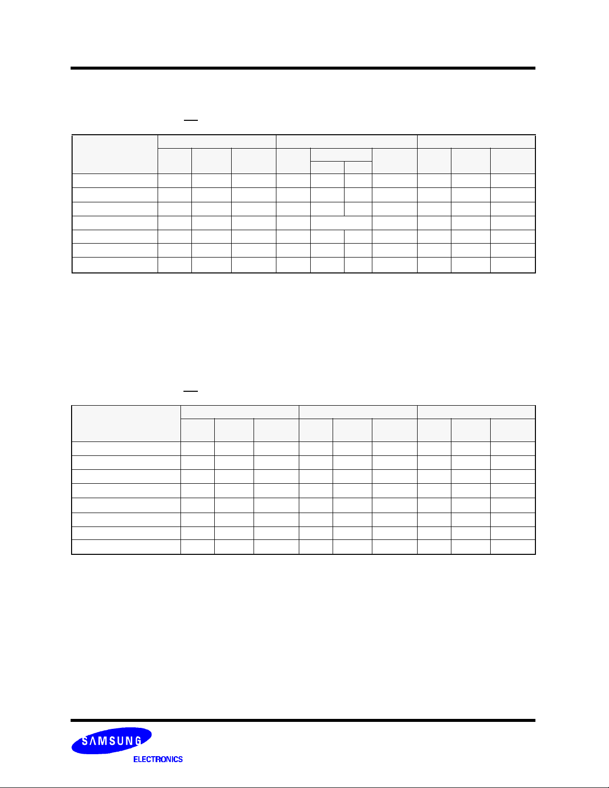
Flash MEMORY COMMAND DEFINITION
Table 3. Command List (F-WP = VIH or VIL)
1st Cycle 2nd Cycle 3rd Cycle
Command
Mode Address
Read Array Write
Sequential Page Read Write
Device Identifier Write
Read Status Register Write
X
X
Bank
Bank
2)
2)
1)
Data
(DQ0-15)
FFH
F3H Read
90H Read
70H Read
Mode
Clear Status Register Write X 50H
Suspend Write
Resume Write
Bank
Bank
2)
B0H
2)
D0H
Notes : 1. Upper byte data (DQ15-DQ8) is ignored.
2. Bank=Bank address (bank1-Bank4:A21-18)
3. IA=ID code address:A0=VIL (Manufacture’s code):A0=VIH (Device code), ID=ID code
4. SRD=Status Register Data
5. SA=Sequential page Address:A21-A3, A2-A0:0h
6. SA+i;A21-A3 must be flxed and A2-A0 must be incremented from 0h to 7h.
Address
A21-A18 A0
5)
SA
2)
Bank
IA
2)
Bank
3)
1)
Data
(DQ0-15)
RD0 Read
ID
4)
SRD
MCP MEMORYK5T6432YT(B)M
Mode Address
6)
SA+i
1)
Data
(DQ0-15)
RDi
Table 4. Command List (F-WP = VIH)
1st Cycle 2nd Cycle 3rd Cycle
Command
Mode Address
Word Program Write Bank 40H Write
Page Program Write Bank 41H Write
Page Buffer to Flash Write Bank 0EH Write
Block Erase / Confirm Write Bank 20H Write
Erase All Unlocked Blocks Write X A7H Write X
Clear Page Buffer Write X 55H Write X
Single Date Load to Page Buffer Write Bank 74H Write WA WD
Flash to Page Buffer Write Bank F1H Write
Notes : 1. Upper byte data (DQ15-DQ8) is ignored.
2. WA=Write Address, WD=Write Data
3. WA0, WAn=Write Address, WD0, WDn=Write Data, Write address and write data must be provided sequentially from 00H to 7FH
for A6-A0. Page size is 128 words (128-word x 16-bit), and also A21-A7(block address, page address) must be valid.
4. WA=Write Address:A21-A7 (block address, page address) must be valid.
5. BA=Block Address:A21-A12(Bank1), A21-A15(Bank2, Bank3, Bank4)
6. RA=Read Address:A21-A7 (block address, page address) must be valid.
1)
Data
(DQ0-15)
Mode Address
WA
WA0
WA
BA
RA
1)
Data
(DQ0-15)
2)
4)
5)
WD
3)
WD0
D0
D0
D0
D0
6)
D0
2)
3)
1)
1)
1)
1)
1)
Mode Address
Write
WAn
Data
(DQ0-15)
3)
WDn
1)
3)
- 11 -
Revision 1.0
November 2001
MCP MEMORYK5T6432YT(B)M
Flash MEMORY COMMAND DEFINITION
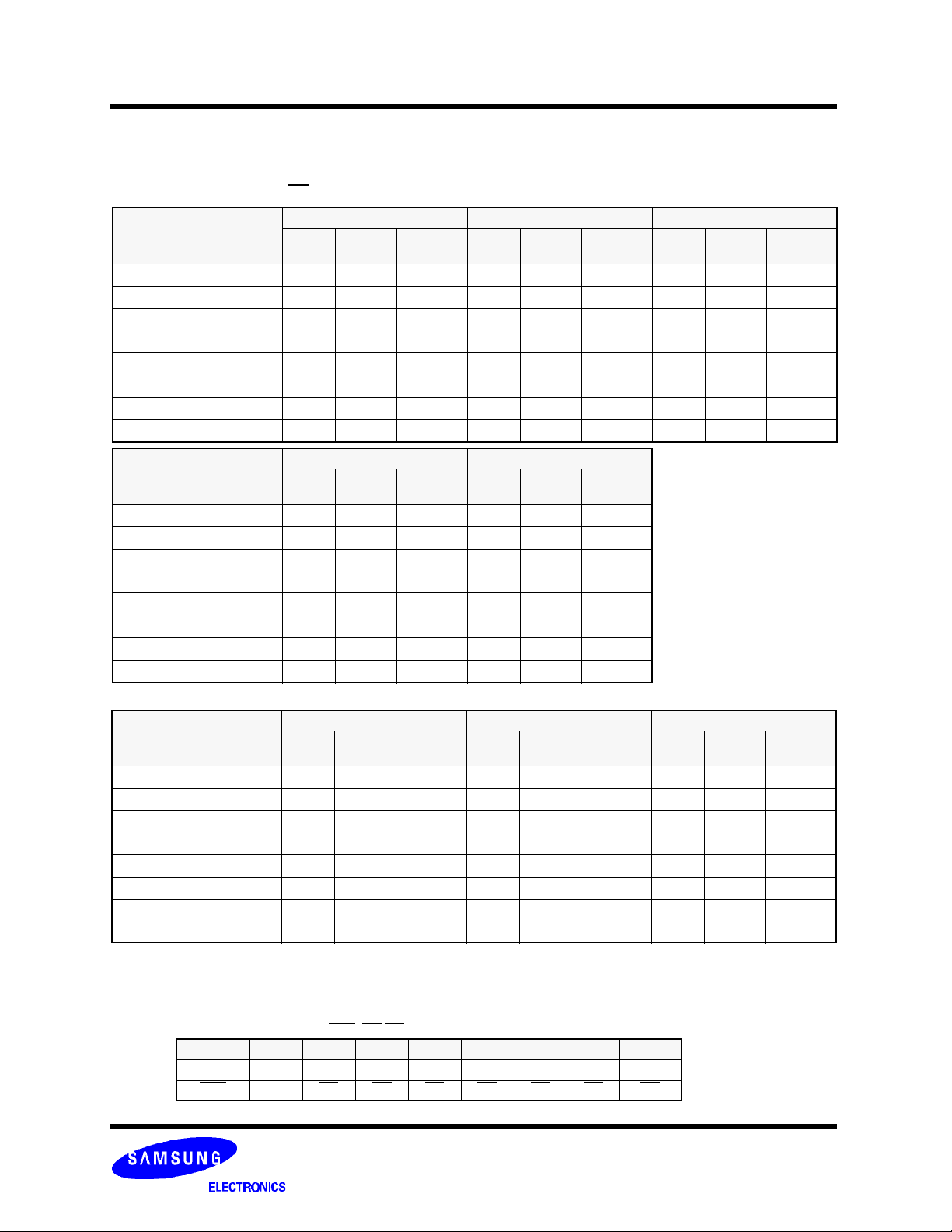
Software lock release operation needs following consecutive 7bus cycles. Moreover, additional 127 bus cycles are needed for page
program operation.
Table 5. Command List (F-WP = VIH or VIL)
Setup Command for
Software Lock Release
Mode Address
Word Program Write Bank 60H Write Bank
Page Program
3)
Write Bank 60H Write Bank
Page Buffer to Flash Write Bank 60H Write Bank
Block Erase / Confirm Write Bank 60H Write Bank
Erase All Unlocked Blocks Write Bank 60H Write Bank
Clear Page Buffer Write Bank 60H Write Bank
Single Data Load to Page Buffer Write Bank 60H Write Bank
Flash to Page Buffer Write Bank 60H Write Bank
1st Cycle 2nd Cycle 3rd Cycle
1)
Data
(DQ0-15)
Mode Address
1)
Data
(DQ0-15)
Block
Block
Block
Block
Block
Block
Block
Block
Mode Address
6)
Write Bank ACH
6)
Write Bank ACH
6)
Write Bank ACH
6)
Write Bank ACH
6)
Write Bank ACH
6)
Write Bank ACH
6)
Write Bank ACH
6)
Write Bank ACH
1)
Data
(DQ0-15)
Setup Command for
Software Lock Release
Mode Address
Word Program Write Bank
Page Program
3)
Write Bank
Page Buffer to Flash Write Bank
Block Erase / Confirm Write Bank
Erase All Unlocked Blocks Write Bank
Clear Page Buffer Write Bank
Single Data Load to Page Buffer Write Bank
Flash to Page Buffer Write Bank
Setup Command for
Software Lock Release
Mode Address
Word Program Write Bank 40h Write
Page Program
3)
Write Bank 41h Write
Page Buffer to Flash Write Bank 0Eh Write
Block Erase / Confirm Write Bank 20H Write
Erase All Unlocked Blocks Write X A7H Write X
Clear Page Buffer Write X 55H Write X
4th Cycle 5th Cycle
1)
Data
(DQ0-15)
6)
Block
6)
Block
6)
Block
6)
Block
6)
Block
6)
Block
6)
Block
6)
Block
Mode Address
Write Bank 78H
Write Bank 78H
Write Bank 78H
Write Bank 78H
Write Bank 78H
Write Bank 78H
Write Bank 78H
Write Bank 78H
1)
Data
(DQ0-15)
6th Cycle 7th Cycle 8th-134th Cycle
1)
Data
(DQ0-15)
Mode Address
WA
WA0
WA
BA
2)
3)
4)
5)
1)
Data
(DQ0-15)
2)
WD
3)
WD0
1)
D0
1)
D0
1)
D0
1)
D0
Mode Address
Write
WAn
3)
Data
(DQ0-15)
WDn
Single Data Load to Page Buffer Write Bank 74H Write WA WD
Flash to Page Buffer Write Bank F1H Write
Notes : 1. Upper byte data (DQ15-DQ8) is ignored.
2. WA=Write Address, WD=Write Data
3. WA0, WAn=Write Address, WD0, WDn=Write Data, Write address and write data must be provided sequentially from 00H to 7FH
for A6-A0. Page size is 128 words (128 word x 16 bit), and also A21-A7(block address, page address) must be valid.
4. WA=Write Address:A21-A7 (block address, page address) must be valid.
5. BA=Block Address:A21-A12(Bank1), A21-A15(Bank2, Bank3, Bank4)
6. Block=Block Address:A21-A15, Block=A21-A15
RA
7)
D0
1)
Address DQ7 DQ6 DQ5 DQ4 DQ3 DQ2 DQ1 DQ0
Block Fixed0 A21 A20 A19 A18 A17 A16 A15
Block Fixed0 A21 A20 A19 A18 A17 A16 A15
7. RA=Read Address: A21-A7 (block address, page address) must be valid.
- 12 -
Revision 1.0
November 2001
1)
3)
 Loading...