

SAMSUNG K4S643233F-S Technical data
现货库存、技术资料、百科信息、热点资讯,精彩尽在鼎好!
K4S643233F-S(D)E/N/I/P
Mobile SDRAM
(VDD/VDDQ 3.0V/3.0V or 3.3V/3.3V)
CMOS SDRAM
2Mx32
90FBGA
Revision 1.5
December 2002
Rev. 1.5 Dec. 2002
K4S643233F-S(D)E/N/I/P
512K x 32Bit x 4 Banks SDRAM
• 3.0V & 3.3 power supply.
• LVCMOS compatible with multiplexed address.
• Four banks operation.
• MRS cycle with address key programs.
-. CAS latency (1, 2 & 3).
-. Burst length (1, 2, 4, 8 & Full page).
-. Burst type (Sequential & Interleave).
• All inputs are sampled at the positive going edge of the system
clock .
• Burst read single-bit write operation.
• DQM for masking.
• Auto & self refresh.
• 64ms refresh period (4K cycle).
• Extended temperature operation (-25°C to 85°C).
Industrial temperature operation ( -40°C to 85°C).
• 90balls FBGA(-SXXX -Pb, -DXXX -Pb Free).
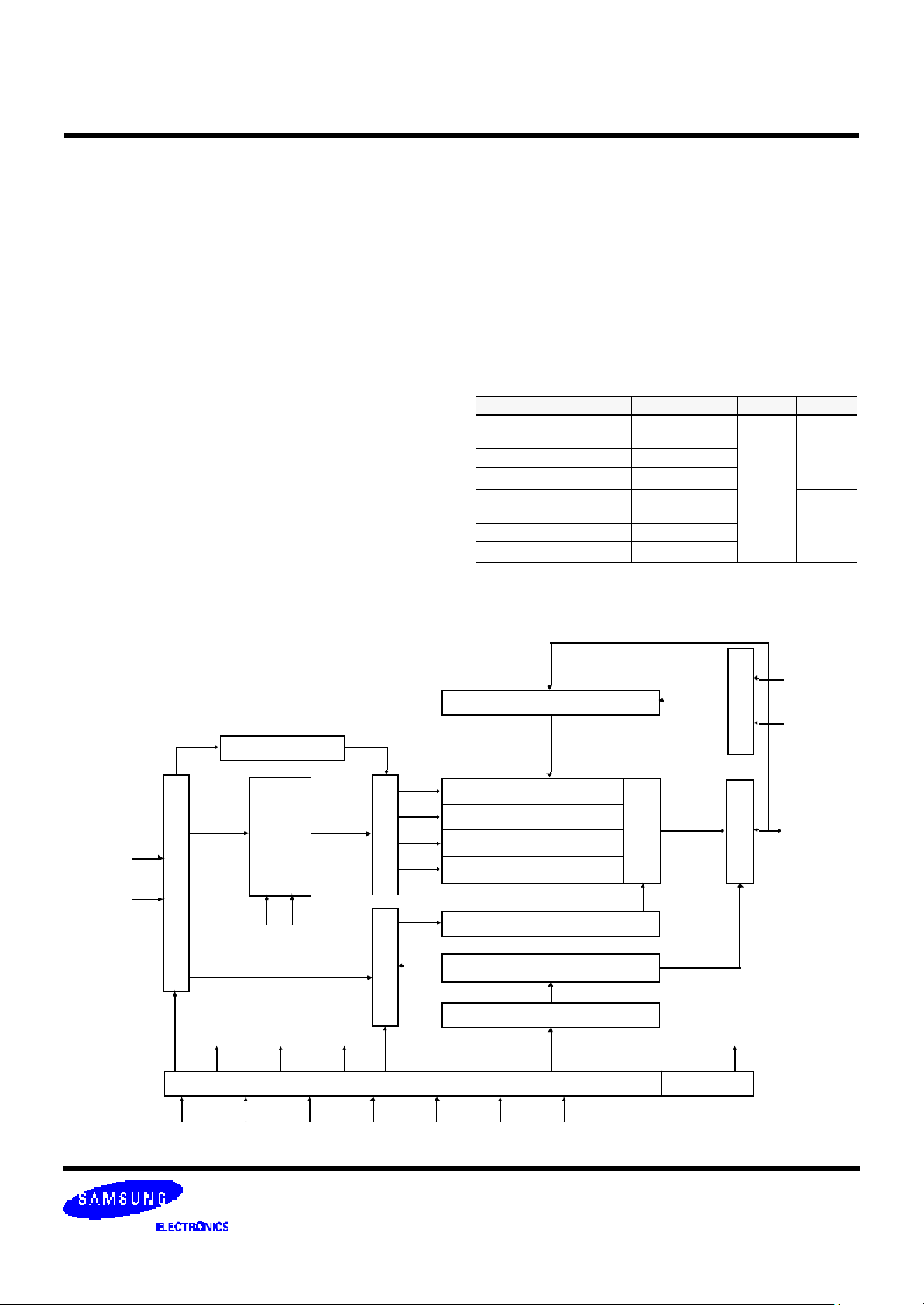
FUNCTIONAL BLOCK DIAGRAM
CMOS SDRAM
GENERAL DESCRIPTIONFEATURES
The K4S643233F is 67,108,864 bits synchronous high data rate
Dynamic RAM organized as 4 x 524,288 words by 32 bits, fabricated with SAMSUNG′s high performance CMOS technology.
Synchronous design allows precise cycle control with the use of
system clock. I/O transactions are possible on every clock cycle.
Range of operating frequencies, programmable burst lengths and
programmable latencies allow the same device to be useful for a
variety of high bandwidth and high performance memory system
applications.
ORDERING INFORMATION
Part No. Max Freq. Interface Package
K4S643233F-SE/N/I/P75
K4S643233FSE/N/I/P1H 105MHz(CL=2)
K4S643233F-SE/N/I/P1L
K4S643233F-DE/N/I/P75
K4S643233F-DE/N/I/P1H 105MHz(CL=2)
K4S643233F-DE/N/I/P1L
-S(D)E/N ; Normal/Low Power, Temp : -25°C ~ 85°C.
-S(D)I/P ; Normal/Low Power, Temp : -40°C ~ 85°C.
Note :
1. In case of 40MHz Frequency, CL1 can be supported.
133MHz(CL=3)
105MHz(CL=2)
105MHz(CL=3)
133MHz(CL=3)
105MHz(CL=2)
105MHz(CL=3)
90FBGA
Pb
*1
LVCMOS
90FBGA
Pb Free
*1
CLK
ADD
LCKE
Data Input Register
Bank Select
Refresh Counter
Row Buffer
Address Register
LRAS
LCBR
LRAS LCBR LWE LDQM
Row Decoder Col. Buffer
LCAS LWCBR
Timing Register
512K x 32
512K x 32
512K x 32
512K x 32
Column Decoder
Latency & Burst Length
Programming Register
Sense AMP
LWE
LDQM
Output BufferI/O Control
DQi
CLK CKE CS RAS CAS WE DQM
*Samsung Electronics reserves the right to change products or specification without notice.
Rev. 1.5 Dec. 2002
K4S643233F-S(D)E/N/I/P
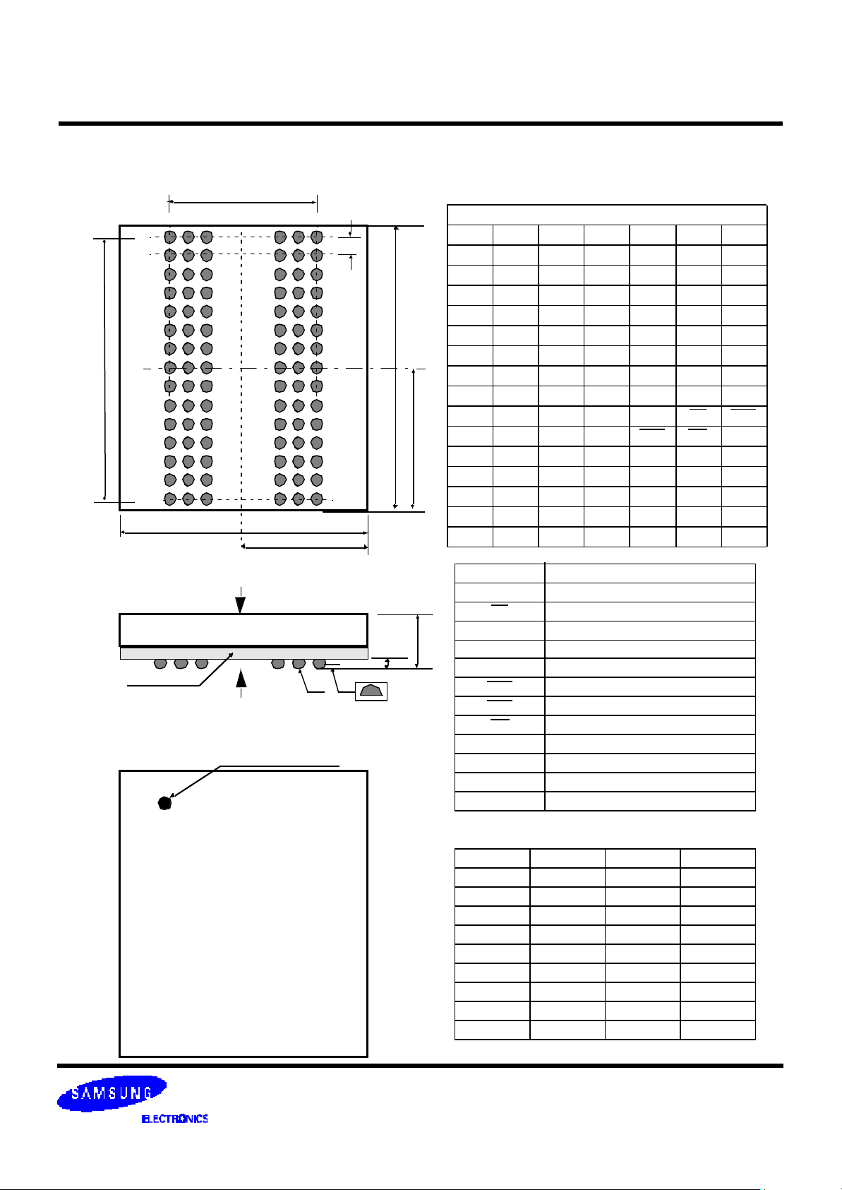
90-Ball FBGA Package Dimension and Pin Configuration
CMOS SDRAM
1
D
Substrate(4Layer)
< Bottom View*1 >
E
1
5 2 16 3489 7
A
B
C
D
E
F
G
H
J
K
L
M
N
P
R
E
*2: Top View
*1: Bottom View
< Top View*2 >
#A1 Ball Origin Indicator
K4S643233F-XXXX
E/2
< Top View*2 >
90Ball(6x15) CSP
e
D
D/2
A
A1
z
b
A DQ26 DQ24 VSS VDD DQ23 DQ21
B DQ28 VDDQ VSSQ VDDQ VSSQ DQ19
C VSSQ DQ27 DQ25 DQ22 DQ20 VDDQ
D VSSQ DQ29 DQ30 DQ17 DQ18 VDDQ
E VDDQ DQ31 NC NC DQ16 VSSQ
F VSS DQM3 A3 A2 DQM2 VDD
G A4 A5 A6 A10 A0 A1
H A7 A8 NC NC BA1 NC
J CLK CKE A9 BA0 CS RAS
K DQM1 NC NC CAS WE DQM0
L VDDQ DQ8 VSS VDD DQ7 VSSQ
M VSSQ DQ10 DQ9 DQ6 DQ5 VDDQ
N VSSQ DQ12 DQ14 DQ1 DQ3 VDDQ
P DQ11 VDDQ VSSQ VDDQ VSSQ DQ4
R DQ13 DQ15 VSS VDD DQ0 DQ2
DQM0 ~ DQM3 Data Input/Output Mask
SAMS UNG Week
VDDQ/VSSQ Data Output Power/Ground
1 2 3 7 8 9
Pin Name Pin Function
CLK System Clock
CS Chip Select
CKE Clock Enable
A0 ~ A10 Address
BA0 ~ BA1 Bank Select Address
RAS Row Address Strobe
CAS Column Address Strobe
WE Write Enable
DQ 0 ~ 31 Data Input/Output
VDD /VSS Power Supply/Ground
[Unit:mm]
Symbol Min Typ Max
A - 1.30 1.40
A
1
E - 11.00 -
E
1
D - 13.00 -
D
1
e - 0.80 b 0.40 0.45 0.50
z - - 0.10
0.30 0.35 0.40
- 6.40 -
- 11.20 -
Rev. 1.5 Dec. 2002
 Loading...