

Samsung K4S643232E-TN50, K4S643232E-TE70, K4S643232E-TE60, K4S643232E-TE50, K4S643232E-TN70 Datasheet
...
K4S643232E-TE/N CMOS SDRAM
2M x 32 SDRAM
512K x 32bit x 4 Banks
Synchronous DRAM
LVTTL(3.3V)
Extended Temperature
86-TSOP
Revision 1.4
December 2001
Samsung Electronics reserves the right to change products or specification without notice.
- 1 -
Rev. 1.4 (Dec. 2001)
K4S643232E-TE/N CMOS SDRAM
Revision History
Revision 1.4 (December 4, 2001)
• Not supported 90-Ball FBGA
Revision 1.3 (October 24, 2001)
• Removed CAS Latency 1 from the spec.
Revision 1.2 (August 7, 2001) - Target
• Added CAS Latency 1
Revision 1.1 (July 6, 2001)
• Added K4S643232E-T/S(E/N)50
Revision 1.0 (April 6, 2001)
Revision 0.0 (March 21, 2001)
• Initial draft
• Extended temperature (-25°c ~ 85°c )
• 3.3V Power supply (VDD &VDDQ)
• Supported 90-ball FBGA as well as 86 - TSOP
- 2 -
Rev. 1.4 (Dec. 2001)
K4S643232E-TE/N CMOS SDRAM
512K x 32Bit x 4 Banks Synchronous DRAM
GENERAL DESCRIPTIONFEATURES
• 3.3V power supply
• LVTTL compatible with multiplexed address
• Four banks operation
• MRS cycle with address key programs
-. CAS latency (2 & 3)
-. Burst length (1, 2, 4, 8 & Full page)
-. Burst type (Sequential & Interleave)
• All inputs are sampled at the positive going edge of the system
clock
• Burst read single-bit write operation
• DQM for masking
• Auto & self refresh
• 15.6us refresh duty cycle(4K/64ms)
• Extended Temperature range : -25oC to +85oC
The K4S643232E is 67,108,864 bits synchronous high data
rate Dynamic RAM organized as 4 x 524,288 words by 32 bits,
fabricated with SAMSUNG′s high performance CMOS technology. Synchronous design allows precise cycle control with the
use of system clock. I/O transactions are possible on every
clock cycle. Range of operating frequencies, programmable
burst length and programmable latencies allow the same device
to be useful for a variety of high bandwidth, high performance
memory system applications.
ORDERING INFORMATION
Part NO. Max Freq. Interface Package
K4S643232E-TE/N50 200MHz
K4S643232E-TE/N60 166MHz
K4S643232E-TE/N70 143MHz
• - E/N : Extended temperature (-25oC - 85oC)
LVTTL
86
TSOP(II)
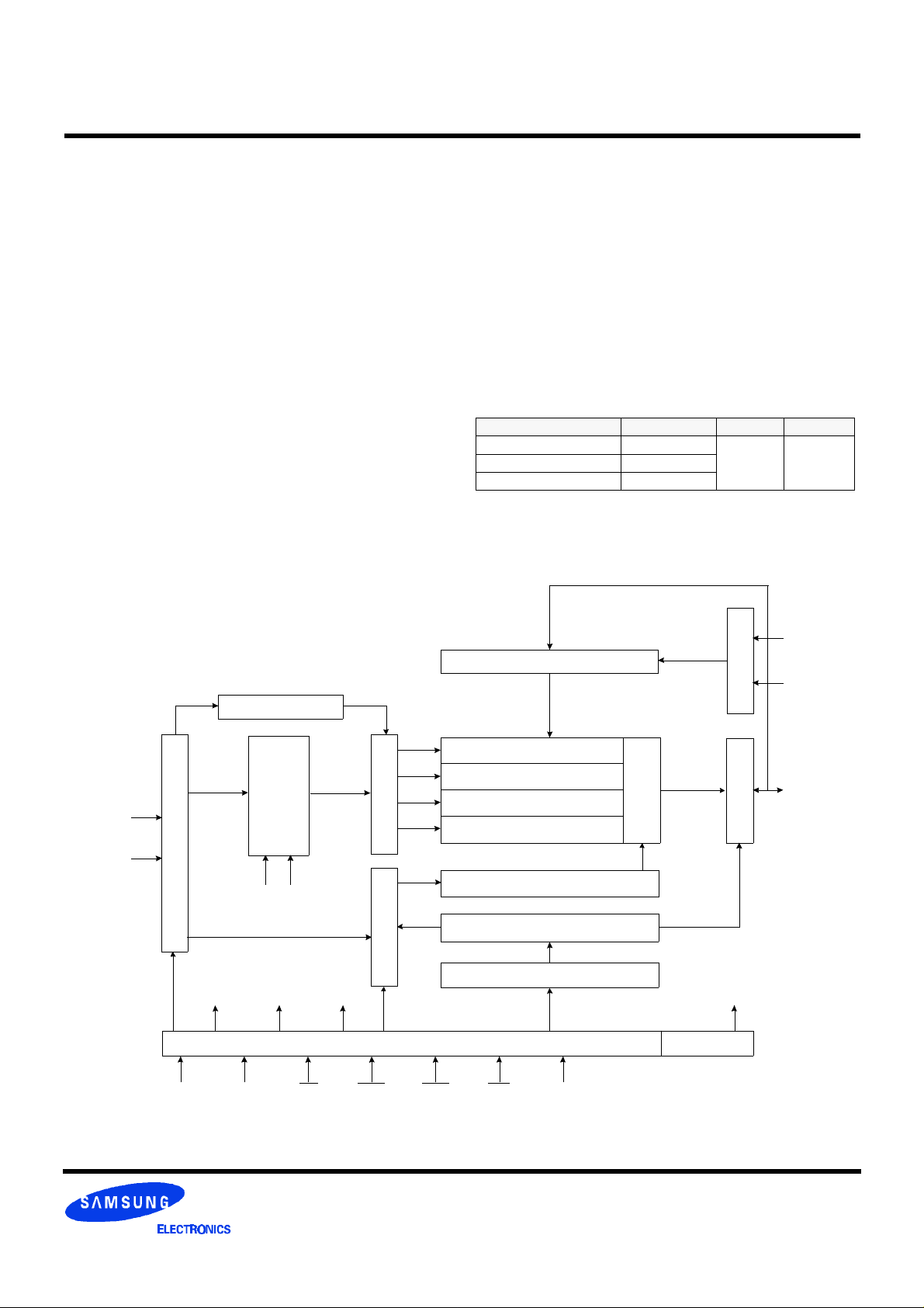
FUNCTIONAL BLOCK DIAGRAM
Bank Select
Refresh Counter
Row Buffer
Address Register
CLK
ADD
LRAS
LCBR
LCKE
LRAS LCBR LWE LDQM
Data Input Register
Row Decoder Col. Buffer
LCAS LWCBR
512K x 32
512K x 32
512K x 32
512K x 32
Column Decoder
Latency & Burst Length
Programming Register
LWE
LDQM
Sense AMP
Output BufferI/O Control
DQi
Timing Register
CLK CKE CS RAS CAS WE DQM
- 3 -
Samsung Electronics reserves the right to
*
change products or specification without
notice.
Rev. 1.4 (Dec. 2001)
K4S643232E-TE/N CMOS SDRAM
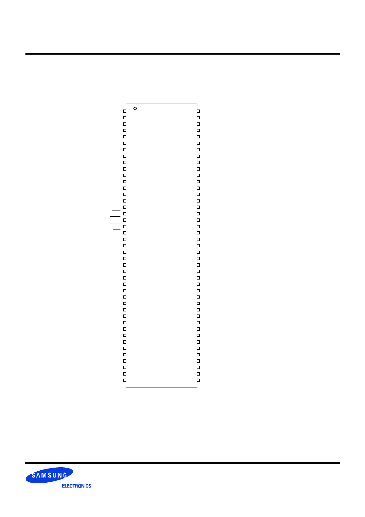
PIN CONFIGURATION (Top view)
86 - TSOP
VDD
DQ0
VDDQ
DQ1
DQ2
VSSQ
DQ3
DQ4
VDDQ
DQ5
DQ6
VSSQ
DQ7
N.C
VDD
DQM0
WE
CAS
RAS
CS
N.C
BA0
BA1
A10/AP
A0
A1
A2
DQM2
VDD
N.C
DQ16
VSSQ
DQ17
DQ18
VDDQ
DQ19
DQ20
VSSQ
DQ21
DQ22
VDDQ
DQ23
VDD
1
2
3
4
5
6
7
8
9
10
11
12
13
14
15
16
17
18
19
20
21
22
23
24
25
26
27
28
29
30
31
32
33
34
35
36
37
38
39
40
41
42
43
86
85
84
83
82
81
80
79
78
77
76
75
74
73
72
71
70
69
68
67
66
65
64
63
62
61
60
59
58
57
56
55
54
53
52
51
50
49
48
47
46
45
44
VSS
DQ15
VSSQ
DQ14
DQ13
VDDQ
DQ12
DQ11
VSSQ
DQ10
DQ9
VDDQ
DQ8
N.C
VSS
DQM1
N.C
N.C
CLK
CKE
A9
A8
A7
A6
A5
A4
A3
DQM3
VSS
N.C
DQ31
VDDQ
DQ30
DQ29
VSSQ
DQ28
DQ27
VDDQ
DQ26
DQ25
VSSQ
DQ24
VSS
86Pin TSOP (II)
(400mil x 875mil)
(0.5 mm Pin pitch)
- 4 -
Rev. 1.4 (Dec. 2001)
 Loading...