

Samsung K4S643232C-TL55, K4S643232C-TL10, K4S643232C-TC80, K4S643232C-TC70, K4S643232C-TC60 Datasheet
...
K4S643232C CMOS SDRAM
2M x 32 SDRAM
512K x 32bit x 4 Banks
Synchronous DRAM
LVTTL
Revision 1.1
November 1999
Samsung Electronics reserves the right to change products or specification without notice.
- 1 -
REV. 1.1 Nov. '99

K4S643232C CMOS SDRAM
Revision History
Revision 1.1 (November 17th, 1999)
• Corrected typo in ordering information on page 3
Revision 1.0 (October, 1999)
• Changed part number from KM432S2030CT-G/F to K4S643232C-TC/TL according to re-organized code system
- 2 -
REV. 1.1 Nov. '99
K4S643232C CMOS SDRAM
512K x 32Bit x 4 Banks Synchronous DRAM
GENERAL DESCRIPTIONFEATURES
• 3.3V power supply
• LVTTL compatible with multiplexed address
• Four banks operation
• MRS cycle with address key programs
-. CAS latency (2 & 3)
-. Burst length (1, 2, 4, 8 & Full page)
-. Burst type (Sequential & Interleave)
• All inputs are sampled at the positive going edge of the system
clock
• Burst read single-bit write operation
• DQM for masking
• Auto & self refresh
• 15.6us refresh duty cycle
The K4S643232C is 67,108,864 bits synchronous high data
rate Dynamic RAM organized as 4 x 524,288 words by 32 bits,
fabricated with SAMSUNG′s high performance CMOS technology. Synchronous design allows precise cycle control with the
use of system clock. I/O transactions are possible on every
clock cycle. Range of operating frequencies, programmable
burst length and programmable latencies allow the same device
to be useful for a variety of high bandwidth, high performance
memory system applications.
ORDERING INFORMATION
Part NO. Max Freq. Interface Package
K4S643232C-TC/L55 183MHz
K4S643232C-TC/L60 166MHz
K4S643232C-TC/L70 143MHz
K4S643232C-TC/L80 125MHz
K4S643232C-TC/L10 100MHz
LVTTL
86
TSOP(II)
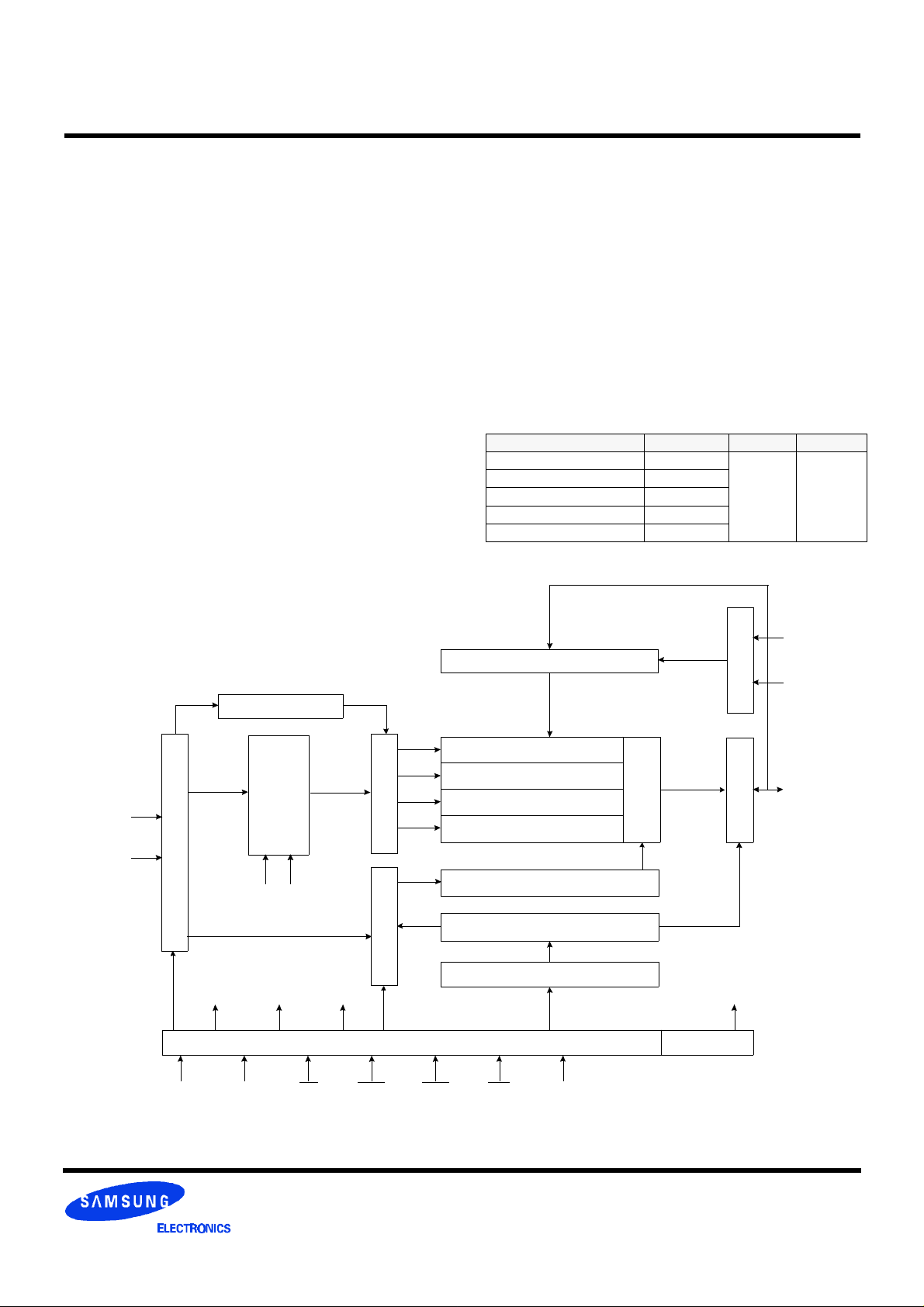
FUNCTIONAL BLOCK DIAGRAM
Bank Select
Refresh Counter
Row Buffer
Address Register
CLK
ADD
LRAS
LCBR
LCKE
LRAS LCBR LWE LDQM
Data Input Register
Row Decoder Col. Buffer
LCAS LWCBR
512K x 32
512K x 32
512K x 32
512K x 32
Column Decoder
Latency & Burst Length
Programming Register
LWE
LDQM
Sense AMP
Output BufferI/O Control
DQi
Timing Register
CLK CKE CS RAS CAS WE DQM
- 3 -
Samsung Electronics reserves the right to
*
change products or specification without
notice.
REV. 1.1 Nov. '99
K4S643232C CMOS SDRAM
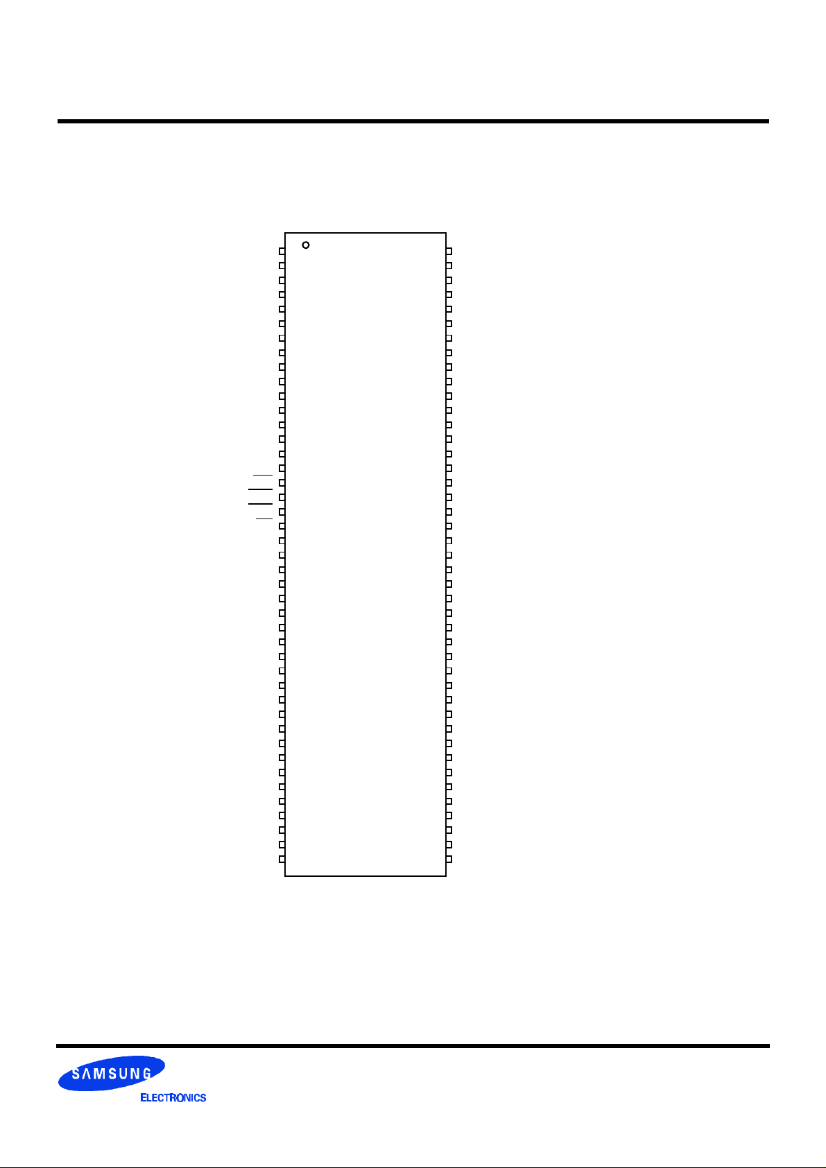
PIN CONFIGURATION (Top view)
VDD
DQ0
VDDQ
DQ1
DQ2
VSSQ
DQ3
DQ4
VDDQ
DQ5
DQ6
VSSQ
DQ7
N.C
VDD
DQM0
WE
CAS
RAS
CS
N.C
BA0
BA1
A10/AP
A0
A1
A2
DQM2
VDD
N.C
DQ16
VSSQ
DQ17
DQ18
VDDQ
DQ19
DQ20
VSSQ
DQ21
DQ22
VDDQ
DQ23
VDD
1
2
3
4
5
6
7
8
9
10
11
12
13
14
15
16
17
18
19
20
21
22
23
24
25
26
27
28
29
30
31
32
33
34
35
36
37
38
39
40
41
42
43
86
85
84
83
82
81
80
79
78
77
76
75
74
73
72
71
70
69
68
67
66
65
64
63
62
61
60
59
58
57
56
55
54
53
52
51
50
49
48
47
46
45
44
VSS
DQ15
VSSQ
DQ14
DQ13
VDDQ
DQ12
DQ11
VSSQ
DQ10
DQ9
VDDQ
DQ8
N.C
VSS
DQM1
N.C
N.C
CLK
CKE
A9
A8
A7
A6
A5
A4
A3
DQM3
VSS
N.C
DQ31
VDDQ
DQ30
DQ29
VSSQ
DQ28
DQ27
VDDQ
DQ26
DQ25
VSSQ
DQ24
VSS
86Pin TSOP (II)
(400mil x 875mil)
(0.5 mm Pin pitch)
- 4 -
REV. 1.1 Nov. '99
K4S643232C CMOS SDRAM
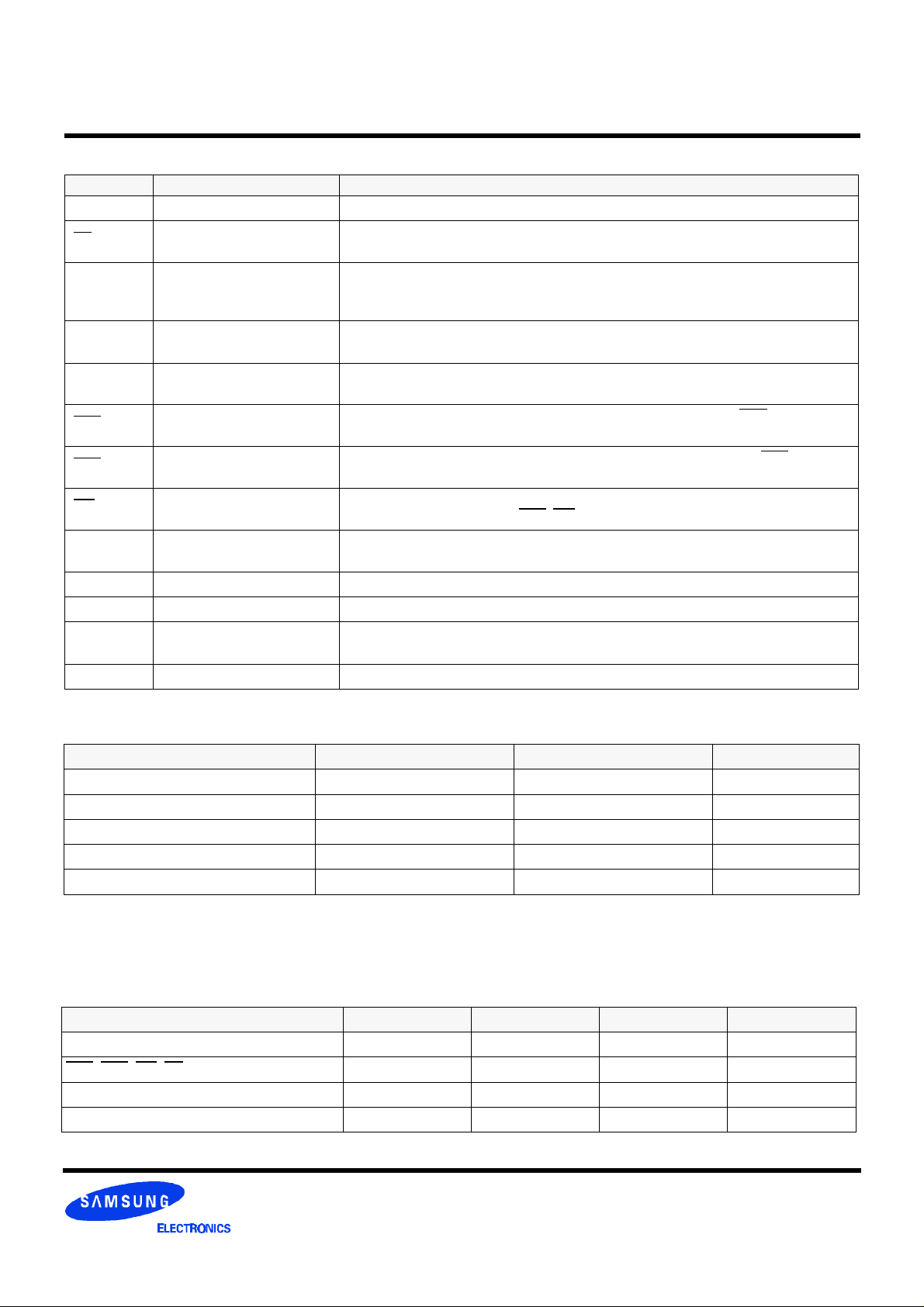
PIN FUNCTION DESCRIPTION
Pin Name Input Function
CLK System clock Active on the positive going edge to sample all inputs.
CS Chip select
CKE Clock enable
A0 ~ A10 Address
BA0,1 Bank select address
RAS Row address strobe
CAS Column address strobe
WE Write enable
DQM0 ~ 3 Data input/output mask
DQ0 ~ 31 Data input/output Data inputs/outputs are multiplexed on the same pins.
VDD/VSS Power supply/ground Power and ground for the input buffers and the core logic.
VDDQ/VSSQ Data output power/ground
NC No Connection This pin is recommended to be left No connection on the device.
Disables or enables device operation by masking or enabling all inputs except
CLK, CKE and DQM.
Masks system clock to freeze operation from the next clock cycle.
CKE should be enabled at least one cycle prior to new command.
Disables input buffers for power down mode.
Row/column addresses are multiplexed on the same pins.
Row address : RA0 ~ RA10, Column address : CA0 ~ CA7
Selects bank to be activated during row address latch time.
Selects bank for read/write during column address latch time.
Latches row addresses on the positive going edge of the CLK with RAS low.
Enables row access & precharge.
Latches column addresses on the positive going edge of the CLK with CAS low.
Enables column access.
Enables write operation and row precharge.
Latches data in starting from CAS, WE active.
Makes data output Hi-Z, tSHZ after the clock and masks the output.
Blocks data input when DQM active.
Isolated power supply and ground for the output buffers to provide improved noise
immunity.
ABSOLUTE MAXIMUM RATINGS
Parameter Symbol Value Unit
Voltage on any pin relative to Vss VIN, VOUT -1.0 ~ 4.6 V
Voltage on VDD supply relative to Vss VDD, VDDQ -1.0 ~ 4.6 V
Storage temperature TSTG -55 ~ +150 °C
Power dissipation PD 1 W
Short circuit current IOS 50 mA
Note :
Permanent device damage may occur if "ABSOLUTE MAXIMUM RATINGS" are exceeded.
Functional operation should be restricted to recommended operating condition.
Exposure to higher than recommended voltage for extended periods of time could affect device reliability.
CAPACITANCE (VDD = 3.3V, TA = 23°C, f = 1MHz, VREF = 1.4V ± 200 mV)
Pin Symbol Min Max Unit
Clock CCLK 2.5 4 pF
RAS, CAS, WE, CS, CKE, DQM CIN 2.5 4.5 pF
Address CADD 2.5 4.5 pF
DQ0 ~ DQ31 COUT 4.0 6.5 pF
- 5 -
REV. 1.1 Nov. '99
K4S643232C CMOS SDRAM
DC OPERATING CONDITIONS
Recommended operating conditions (Voltage referenced to VSS = 0V, TA = 0 to 70°C)
Parameter Symbol Min Typ Max Unit Note
Supply voltage VDD, VDDQ 3.0 3.3 3.6 V 4
Input logic high voltage VIH 2.0 3.0 VDDQ+0.3 V 1
Input logic low voltage VIL -0.3 0 0.8 V 2
Output logic high voltage VOH 2.4 - - V IOH = -2mA
Output logic low voltage VOL - - 0.4 V IOL = 2mA
Input leakage current ILI -10 - 10 uA 3
Notes :
1. VIH (max) = 5.6V AC.The overshoot voltage duration is ≤ 3ns.
2. VIL (min) = -2.0V AC. The undershoot voltage duration is ≤ 3ns.
3. Any input 0V ≤ VIN ≤ VDDQ,
Input leakage currents include Hi-Z output leakage for all bi-directional buffers with Tri-State outputs.
4. The VDD condition of K4S643232C-55/60 is 3.135V~3.6V.
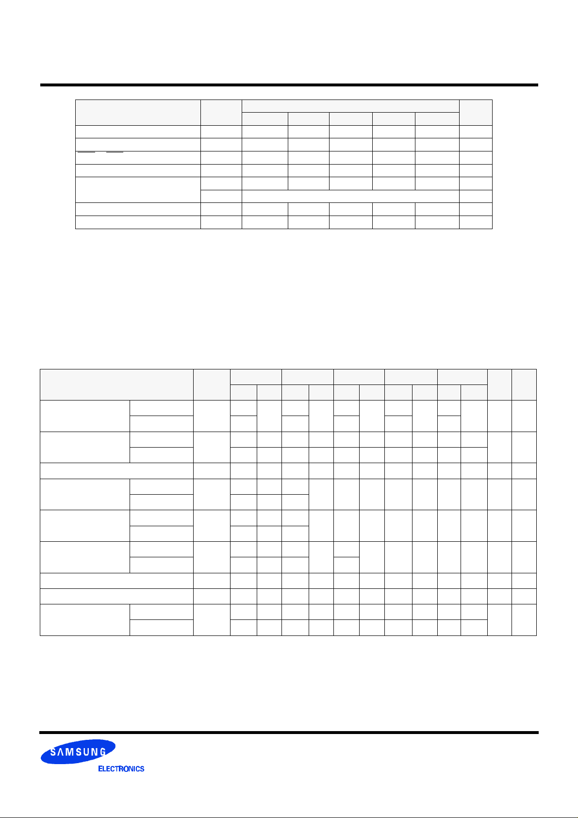
DC CHARACTERISTICS
(Recommended operating condition unless otherwise noted, TA = 0 to 70°C)
Parameter Symbol Test Condition
Operating current
(One bank active)
Precharge standby current
in power-down mode
Precharge standby current
in non power-down mode
Active standby current in
power-down mode
Active standby current in
non power-down mode
(One bank active)
Operating current
(Burst mode)
Refresh current ICC5 tRC ≥ tRC(min)
Self refresh current ICC6 CKE ≤ 0.2V
Notes :
1. Unless otherwise notes, Input level is CMOS(VIH/VIL=VDDQ/VSSQ) in LVTTL.
2. Measured with outputs open.
3. Refresh period is 64ms.
4. K4S643232C-TC**
5. K4S643232C-TL**
ICC2P CKE ≤ VIL(max), tCC = 15ns 2
ICC2PS CKE & CLK ≤ VIL(max), tCC = ∞ 2
ICC2N
ICC2NS
ICC3P CKE ≤ VIL(max), tCC = 15ns 3
ICC3PS CKE & CLK ≤ VIL(max), tCC = ∞ 3
ICC3N
ICC3NS
Burst length = 1
ICC1
tRC ≥ tRC(min)
Io = 0 mA
CKE ≥ VIH(min), CS ≥ VIH(min), tCC = 15ns
Input signals are changed one time during 30ns
CKE ≥ VIH(min), CLK ≤ VIL(max), tCC = ∞
Input signals are stable
CKE ≥ VIH(min), CS ≥ VIH(min), tCC = 15ns
Input signals are changed one time during 30ns
CKE ≥ VIH(min), CLK ≤ VIL(max), tCC = ∞
Input signals are stable
Io = 0 mA
Page burst
ICC4
2 Banks activated
CAS
Latency
-55 -60 -70 -80 -10
3 140 140 130 130 115
2 - - - 130 115
3 220 200 180 150 130
2 - - - 130 110
3 200 200 180 160 150
2 - - - 160 150
Version
20 mA
10 mA
30 mA
20 mA
2 mA 4
450 uA 5
Unit Note
mA 2
mA
mA
mA 2
mA 3
- 6 -
REV. 1.1 Nov. '99
K4S643232C CMOS SDRAM
AC OPERATING TEST CONDITIONS (VDD = 3.3V ± 0.3V, TA = 0 to 70°C)
Parameter Value Unit
AC input levels (Vih/Vil) 2.4/0.4 V
Input timing measurement reference level 1.4 V
Input rise and fall time tr/tf = 1/1 ns
Output timing measurement reference level 1.4 V
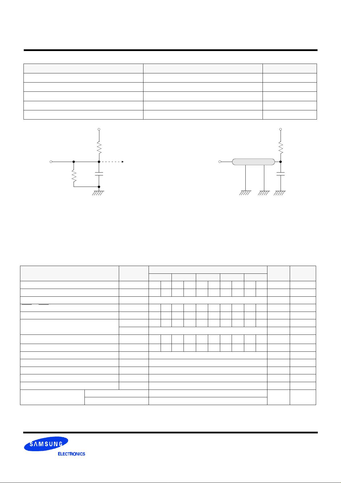
Output load condition See Fig. 2
3.3V
1200Ω
Output
870Ω
Note :
1. The DC/AC Test Output Load of K4S643232C-55/60/70 is 30pF.
2. The VDD condition of K4S643232C-55/60 is 3.135V~3.6V.
50pF
VOH (DC) = 2.4V, IOH = -2mA
VOL (DC) = 0.4V, IOL = 2mA
*1
Output
Z0 = 50Ω
(Fig. 2) AC output load circuit (Fig. 1) DC output load circuit
Vtt = 1.4V
50Ω
*1
50pF
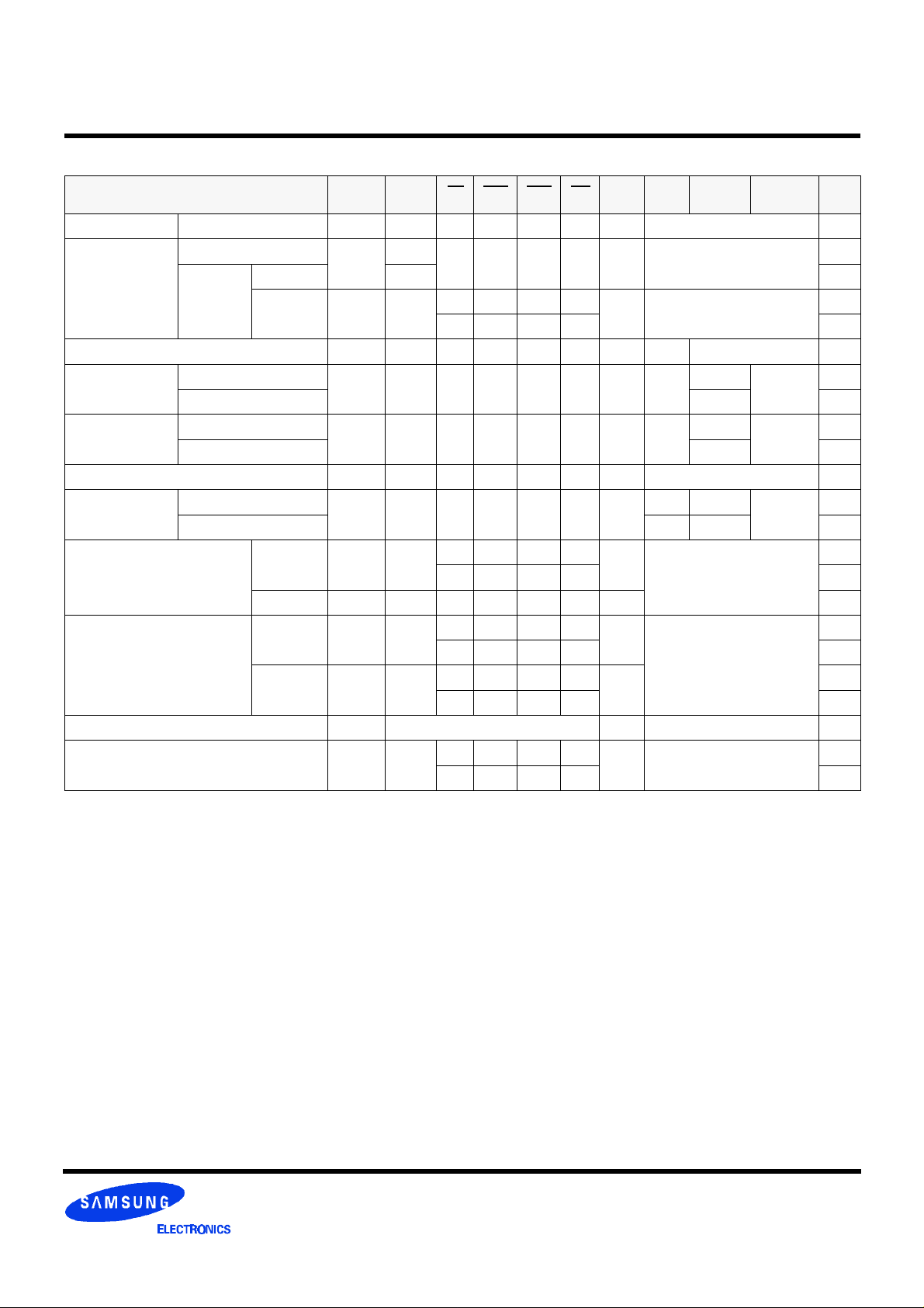
OPERATING AC PARAMETER
(AC operating conditions unless otherwise noted)
Parameter Symbol
CAS Latency CL 3 2 3 2 3 2 3 2 3 2 CLK
CLK cycle time tCC(min) 5.5 - 6 - 7 - 8 10 10 12 ns
Row active to row active delay tRRD(min) 2 CLK 1
RAS to CAS delay tRCD(min) 3 - 3 - 3 - 3 2 2 2 CLK 1
Row precharge time tRP(min) 3 - 3 - 3 - 3 2 2 2 CLK 1
Row active time
Row cycle time
Row cycle time in Auto refresh tRFC(min) 12 - 12 - 10 - 9 7 7 6 CLK 1,6
Last data in to row precharge tRDL(min) 2 CLK 2, 5
Last data in to new col.address delay tCDL(min) 1 CLK 2
Last data in to burst stop tBDL(min) 1 CLK 2
Col. address to col. address delay tCCD(min) 1 CLK
Mode Register Set cycle time tMRS(min) 2 CLK
Number of valid output data
CAS Latency=3 2
CAS Latency=2 1
tRAS(min) 7 - 7 - 7 - 6 5 5 4 CLK 1
tRAS(max) 100 us
tRC(min) 10 - 10 - 10 - 9 7 7 6 CLK 1
-55 -60 -70 -80 -10
Version
Unit Note
ea 4
Note :
1. The minimum number of clock cycles is determined by dividing the minimum time required with clock cycle time and then
rounding off to the next higher integer. Refer to the following ns-unit based AC table.
- 7 -
REV. 1.1 Nov. '99
K4S643232C CMOS SDRAM
Parameter Symbol
CLK cycle time tCC(min) 5.5 6 7 8 10 ns
Row active to row active delay tRRD(min) 11 12 14 16 20 ns
RAS to CAS delay tRCD(min) 16.5 18 21 20 20 ns
Row precharge time tRP(min) 16.5 18 21 20 20 ns
Row active time
Row cycle time tRC(min) 55 60 70 70 70 ns
Row cycle time in Auto refresh tRFC(min) 66 72 70 70 70 ns
2. Minimum delay is required to complete write.
3. All parts allow every cycle column address change.
4. In case of row precharge interrupt, auto precharge and read burst stop.
5. For -55/60/70/80/10, tRDL=1CLK product can be supported within restricted amounts and it will be distinguished by bucket
code "NV". From the next generation, tRDL will be only 2CLK for every clock frequency.
6. A new command should be issued after self refersh exit followed by tRFC.
tRAS(min) 38.5 42 49 48 48 ns
tRAS(max) 100 us
-55 -60 -70 -80 -10
Version
Unit
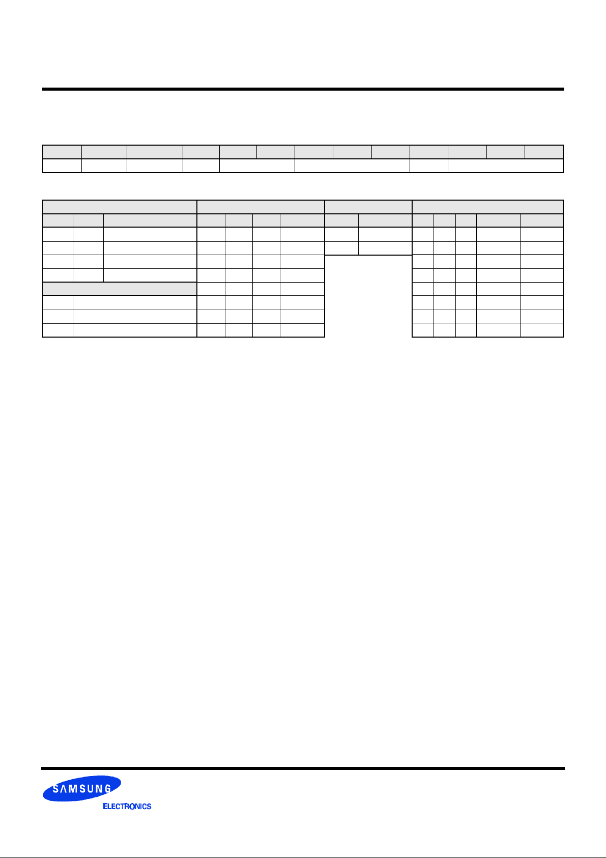
AC CHARACTERISTICS (AC operating conditions unless otherwise noted)
Parameter Symbol
CLK cycle time
CLK to valid
output delay
Output data tOH 2 - 2.5 - 2.5 - 2.5 - 2.5 - ns 2
CLK high pulse width
CLK low pulse width
Input setup time
Input hold time tSH 1 - 1 - 1 - 1 - 1 - ns 3
CLK to output in Low-Z tSLZ 1 - 1 - 1 - 1 - 1 - ns 2
CLK to output
in Hi-Z
CAS Latency=3
CAS Latency=2 - - - 10 12
CAS Latency=3
CAS Latency=2 - - - - - - - 6 - 8
CAS Latency=3
CAS Latency=2 - CAS Latency=3
CAS Latency=2 - CAS Latency=3
CAS Latency=2 - -
CAS Latency=3
CAS Latency=2 - - - - - - - 6 - 8
tCC
tSAC
tCH
tCL
tSS
tSHZ
-55 -60 -70 -80 -10
Min Max Min Max Min Max Min Max Min Max
5.5
1000
- 5 - 5.5 - 5.5 - 6 - 6
2 - 2.5
2 - 2.5
1.5 - 1.5
- 5 - 5.5 - 5.5 - 6 - 6
6
1000
-
-
-
7
1000
- 3 - 3 - 3.5 - ns 3
- 3 - 3 - 3.5 - ns 3
1.75
-
-
8
- 2 - 2.5 - ns 3
1000
10
1000 ns 1
Unit Note
ns 1, 2
ns
Note :
1. Parameters depend on programmed CAS latency.
2. If clock rising time is longer than 1ns, (tr/2-0.5)ns should be added to the parameter.
3. Assumed input rise and fall time (tr & tf)=1ns.
If tr & tf is longer than 1ns, transient time compensation should be considered,
i.e., [(tr + tf)/2-1]ns should be added to the parameter.
- 8 -
REV. 1.1 Nov. '99
K4S643232C CMOS SDRAM
SIMPLIFIED TRUTH TABLE
Command CKEn-1 CKEn CS RAS CAS WE DQM BA0,1 A10/AP
Register Mode register set H X L L L L X OP code 1,2
Auto refresh
Refresh
Bank active & row addr. H X L L H H X V Row address
Read &
column address
Write &
column address
Burst Stop H X L H H L X X 6
Precharge
Clock suspend or
active power down
Precharge power down mode
DQM H V X 7
No operation command H X
(V=Valid, X=Don′t care, H=Logic high, L=Logic low)
Notes :
1. OP Code : Operand code
A0 ~ A10 & BA0 ~ BA1 : Program keys. (@ MRS)
2. MRS can be issued only at all banks precharge state.
A new command can be issued after 2 CLK cycles of MRS.
3. Auto refresh functions are as same as CBR refresh of DRAM.
The automatical precharge without row precharge command is meant by "Auto".
Auto/self refresh can be issued only at all banks precharge state.
4. BA0 ~ BA1 : Bank select addresses.
If both BA0 and BA1 are "Low" at read, write, row active and precharge, bank A is selected.
If both BA0 is "Low" and BA1 is "High" at read, write, row active and precharge, bank B is selected.
If both BA0 is "High" and BA1 is "Low" at read, write, row active and precharge, bank C is selected.
If both BA0 and BA1 are "High" at read, write, row active and precharge, bank D is selected.
If A10/AP is "High" at row precharge, BA0 and BA1 is ignored and all banks are selected.
5. During burst read or write with auto precharge, new read/write command can not be issued.
Another bank read/write command can be issued after the end of burst.
New row active of the associated bank can be issued at tRP after the end of burst.
6. Burst stop command is valid at every burst length.
7. DQM sampled at positive going edge of a CLK and masks the data-in at the very CLK (Write DQM latency is 0),
but makes Hi-Z state the data-out of 2 CLK cycles after. (Read DQM latency is 2)
Self
refresh
Auto precharge disable
Auto precharge enable H 4,5
Auto precharge disable
Auto precharge enable H 4,5
Bank selection
All banks X H
Entry L 3
Exit L H
Entry H L
Exit L H X X X X X
Entry H L
Exit L H
H
H X L H L H X V
H X L H L L X V
H X L L H L X
H
L L L H X X
L H H H
H X X X 3
H X X X
L V V V
H X X X
L H H H
H X X X
L V V V
X
H X X X
L H H H
X X
L
L
V L
X
X
X
X
X
X X
,
A9 ~ A0
Column
address
(A0 ~ A7)
Column
address
(A0 ~ A7)
X
Note
3
3
4
4
- 9 -
REV. 1.1 Nov. '99
K4S643232C CMOS SDRAM
MODE REGISTER FIELD TABLE TO PROGRAM MODES
Register Programmed with MRS
Address
Function
A8 A7 A6 A5 A4 A3 A2 A1 A0 BT = 0
A9
BA0 ~ BA1
RFU
Test Mode
0
0
1
1
0
1
0
1
0
1
Write Burst Length
A10/AP
RFU
Type
Mode Register Set
Reserved
Reserved
Reserved
Length
Burst
Single Bit
A9
W.B.L
0
0
0
0
1
1
1
1
A8 A7
TM
CAS Latency
0
0
0
1
1
0
1
1
0
0
0
1
1
0
1
1
A6 A5 A4 A3 A2 A1 A0
CAS Latency BT Burst Length
Latency
Reserved
Reserved
2
3
Reserved
Reserved
Reserved
Reserved
Burst Type
0
Sequential
1
Interleave
Type
0
0
0
0
1
1
1
1
Burst Length
0
0
0
1
1
0
1
1
0
0
1
1
Full Page Length : x32 (256)
Reserved
0
Reserved
1
Reserved
0
Full Page
1
POWER UP SEQUENCE
SDRAMs must be powered up and initialized in a predefined manner to prevent undefined operations.
1. Apply power and start clock. Must maintain CKE= "H", DQM= "H" and the other pins are NOP condition at the inputs.
2. Maintain stable power, stable clock and NOP input condition for a minimum of 200us.
3. Issue precharge commands for all banks of the devices.
4. Issue 2 or more auto-refresh commands.
5. Issue a mode register set command to initialize the mode register.
cf.) Sequence of 4 & 5 is regardless of the order.
1
2
4
8
BT = 1
1
2
4
8
Reserved
Reserved
Reserved
Reserved
The device is now ready for normal operation.
Note : 1. If A9 is high during MRS cycle, "Burst Read Single Bit Write" function will be enabled.
2. RFU (Reserved for future use) should stay "0" during MRS cycle.
- 10
REV. 1.1 Nov. '99
K4S643232C CMOS SDRAM
BURST SEQUENCE (BURST LENGTH = 4)
Initial Address
A1 A0
0
0
1
1
0
1
0
1
0
1
2
3
BURST SEQUENCE (BURST LENGTH = 8)
Initial Address
A1 A0A2
0
0
0
0
1
1
1
1
0
0
1
1
0
0
1
1
0
1
0
1
0
1
0
1
0
1
1
2
2
3
3
4
4
5
5
6
6
7
7
0
Sequential Interleave
1
2
3
0
Sequential Interleave
2
3
3
4
4
5
5
6
6
7
7
0
0
1
1
2
2
3
0
1
4
5
5
6
6
7
7
0
0
1
1
2
2
3
3
4
3
0
1
2
6
7
7
0
0
1
1
2
2
3
3
4
4
5
5
6
0
1
2
3
0
1
2
3
4
5
6
7
2
1
3
0
0
3
1
2
6
5
7
4
4
7
5
6
1
0
3
2
3
2
1
0
7
6
5
4
2
3
0
1
4
5
5
4
6
7
7
6
0
1
1
0
2
3
3
2
3
2
1
0
6
7
7
6
4
5
5
4
2
3
3
2
0
1
1
0
- 11
REV. 1.1 Nov. '99
K4S643232C CMOS SDRAM
DEVICE OPERATIONS
CLOCK (CLK)
The clock input is used as the reference for all SDRAM operations. All operations are synchronized to the positive going edge
of the clock. The clock transitions must be monotonic between
VIL and VIH. During operation with CKE high all inputs are
assumed to be in a valid state (low or high) for the duration of
set-up and hold time around positive edge of the clock in order
to function well Q perform and ICC specifications.
CLOCK ENABLE (CKE)
The clock enable(CKE) gates the clock onto SDRAM. If CKE
goes low synchronously with clock (set-up and hold time are thesame as other inputs), the internal clock is suspended from the
next clock cycle and the state of output and burst address is frozen as long as the CKE remains low. All other inputs are ignored
from the next clock cycle after CKE goes low. When all banks
are in the idle state and CKE goes low synchronously with clock,
the SDRAM enters the power down mode from the next clock
cycle. The SDRAM remains in the power down mode ignoring
the other inputs as long as CKE remains low. The power down
exit is synchronous as the internal clock is suspended. When
CKE goes high at least "1CLK + tSS" before the high going edge
of the clock, then the SDRAM becomes active from the same
clock edge accepting all the input commands.
NOP and DEVICE DESELECT
When RAS, CAS and WE are high, the SDRAM performs no
operation (NOP). NOP does not initiate any new operation, but
is needed to complete operations which require more than single clock cycle like bank activate, burst read, auto refresh, etc.
The device deselect is also a NOP and is entered by asserting
CS high. CS high disables the command decoder so that RAS,
CAS, WE and all the address inputs are ignored.
POWER-UP
SDRAMs must be powered up and initialized in a predefined manner to prevent undefined operations.
1. Apply power and start clock. Must maintain CKE= "H", DQM=
"H" and the other pins are NOP condition at the inputs.
2. Maintain stable power, stable clock and NOP input condition
for a minimum of 200us.
3. Issue precharge commands for both banks of the devices.
4. Issue 2 or more auto-refresh commands.
5. Issue a mode register set command to initialize the mode reg ister.
cf.) Sequence of 4 & 5 is regardless of the order.
BANK ADDRESSES (BA0 ~ BA1)
This SDRAM is organized as four independent banks of 524,288
words x 32 bits memory arrays. The BA0 ~ BA1 inputs are
latched at the time of assertion of RAS and CAS to select the
bank to be used for the operation. The bank addresses BA0 ~
BA1 are latched at bank active, read, write, mode register set
and precharge operations.
ADDRESS INPUTS (A0 ~ A10)
The 19 address bits are required to decode the 524,288 word
locations are multiplexed into 11 address input pins (A0 ~ A10).
The 11 bit row addresses are latched along with RAS and BA0 ~
BA1 during bank activate command. The 8 bit column addresses
are latched along with CAS, WE and BA0 ~ BA1 during read or
write command.
The device is now ready for normal operation.
- 12
REV. 1.1 Nov. '99

K4S643232C CMOS SDRAM
DEVICE OPERATIONS (Continued)
MODE REGISTER SET (MRS)
The mode register stores the data for controlling the various
operating modes of SDRAM. It programs the CAS latency, burst
type, burst length, test mode and various vendor specific options
to make SDRAM useful for variety of different applications. The
default value of the mode register is not defined, therefore the
mode register must be written after power up to operate the
SDRAM. The mode register is written by asserting low on CS,
RAS, CAS and WE (The SDRAM should be in active mode with
CKE already high prior to writing the mode register). The state of
address pins A0 ~ A10 and BA0 ~ BA1 in the same cycle as CS,
RAS, CAS and WE going low is the data written in the mode
register. Two clock cycles is required to complete the write in the
mode register. The mode register contents can be changed
using the same command and clock cycle requirements during
operation as long as all banks are in the idle state. The mode
register is divided into various fields depending on the fields of
functions. The burst length field uses A0 ~ A2, burst type uses
A3, CAS latency (read latency from column address) use A4 ~
A6, vendor specific options or test mode use A7 ~ A8, A10/AP
and BA0 ~ BA1. The write burst length is programmed using A9.
A7 ~ A8, A10/AP and BA0 ~ BA1 must be set to low for normal
SDRAM operation. Refer to the table for specific codes for various burst length, burst type and CAS latencies.
BANK ACTIVATE
The bank activate command is used to select a random row in
an idle bank. By asserting low on RAS and CS with desired row
and bank address, a row access is initiated. The read or write
operation can occur after a time delay of tRCD(min) from the time
of bank activation. tRCD is an internal timing parameter of
SDRAM, therefore it is dependent on operating clock frequency.
The minimum number of clock cycles required between bank
activate and read or write command should be calculated by
dividing tRCD(min) with cycle time of the clock and then rounding
off the result to the next higher integer. The SDRAM has four
internal banks in the same chip and shares part of the internal
circuitry to reduce chip area, therefore it restricts the activation
of four banks simultaneously. Also the noise generated during
sensing of each bank of SDRAM is high, requiring some time for
power supplies to recover before another bank can be sensed
reliably. tRRD(min) specifies the minimum time required between
activating different bank. The number of clock cycles required
between different bank activation must be calculated similar to
tRCD specification. The minimum time required for the bank to be
active to initiate sensing and restoring the complete row of
dynamic cells is determined by tRAS(min). Every SDRAM bank
activate command must satisfy tRAS(min) specification before a
precharge command to that active bank can be asserted. The
maximum time any bank can be in the active state is determined
by tRAS(max). The number of cycles for both tRAS(min) and
tRAS(max) can be calculated similar to tRCD specification.
BURST READ
The burst read command is used to access burst of data on consecutive clock cycles from an active row in an active bank. The
burst read command is issued by asserting low on CS and CAS
with WE being high on the positive edge of the clock. The bank
must be active for at least tRCD(min) before the burst read command is issued. The first output appears in CAS latency number
of clock cycles after the issue of burst read command. The burst
length, burst sequence and latency from the burst read command is determined by the mode register which is already programmed. The burst read can be initiated on any column
address of the active row. The address wraps around if the initial
address does not start from a boundary such that number of outputs from each I/O are equal to the burst length programmed in
the mode register. The output goes into high-impedance at the
end of the burst, unless a new burst read was initiated to keep
the data output gapless. The burst read can be terminated by
issuing another burst read or burst write in the same bank or the
other active bank or a precharge command to the same bank.
The burst stop command is valid at every page burst length.
BURST WRITE
The burst write command is similar to burst read command and
is used to write data into the SDRAM on consecutive clock
cycles in adjacent addresses depending on burst length and
burst sequence. By asserting low on CS, CAS and WE with valid
column address, a write burst is initiated. The data inputs are
provided for the initial address in the same clock cycle as the
burst write command. The input buffer is deselected at the end
of the burst length, even though the internal writing can be completed yet. The writing can be completed by issuing a burst read
and DQM for blocking data inputs or burst write in the same or
another active bank. The burst stop command is valid at every
burst length. The write burst can also be terminated by using
DQM for blocking data and procreating the bank tRDL after the
last data input to be written into the active row. See DQM
OPERATION also.
- 13
REV. 1.1 Nov. '99
 Loading...