

SAMSUNG K4S641633H Technical data
查询K4S641633H-C供应商
K4S641633H - R(B)E/N/G/C/L/F
1M x 16Bit x 4 Banks Mobile SDRAM in 54FBGA
FEATURES
• 3.0V & 3.3V power supply.
• LVCMOS compatible with multiplexed address.
• Four banks operation.
• MRS cycle with address key programs.
-. CAS latency (1, 2 & 3).
-. Burst length (1, 2, 4, 8 & Full page).
-. Burst type (Sequential & Interleave).
• EMRS cycle with address key programs.
• All inputs are sampled at the positive going edge of the system
clock.
• Burst read single-bit write operation.
• Special Function Support.
-. PASR (Partial Array Self Refresh).
-. Internal TCSR (Temperature Compensated Self Refresh)
• DQM for masking.
• Auto refresh.
• 64ms refresh period (4K cycle).
• Commercial Temperature Operation (-25°C ~ 70°C).
• Extended Temperature Operation (-25°C ~ 85°C).
• 54Balls FBGA with 0.8mm ball pitch
( -RXXX : Leaded, -BXXX : Lead Free).
Mobile-SDRAM
GENERAL DESCRIPTION
The K4S641633H is 67,108,864 bits synchronous high data
rate Dynamic RAM organized as 4 x 1,048,576 words by 16 bits,
fabricated with SAMSUNG’s high performance CMOS technology. Synchronous design allows precise cycle control with the
use of system clock and I/O transactions are possible on every
clock cycle. Range of operating frequencies, programmable
burst lengths and programmable latencies allow the same
device to be useful for a variety of high bandwidth and high performance memory system applications.
ORDERING INFORMATION
Part No. Max Freq. Interface Package
K4S641633H-R(B)E/N/G/C/L/F75 133MHz(CL=3)
K4S641633H-R(B)E/N/G/C/L/F1H 105MHz(CL=2)
K4S641633H-R(B)E/N/G/C/L/F1L
- R(B)E/N/G : Normal / Low / Low Power, Extended Temperature(-25°C ~ 85°C)
- R(B)C/L/F : Normal / Low / Low Power, Commercial Temperature(-25°C ~ 70°C)
NOTES :
1. In case of 40MHz Frequency , CL1 can be supported.
2. Samsung are not designed or manufactured for use in a device or system that is used under circumstance in which human life is potentially at stake.
Please contact to the memory marketing team in samsung electronics when considering the use of a product contained herein for any specific
purpose, such as medical, aerospace, nuclear, military, vehicular or undersea repeater use.
105MHz(CL=3)
*1
LVCMOS
54 FBGA
Leaded (Lead Free)
February 2004
K4S641633H - R(B)E/N/G/C/L/F
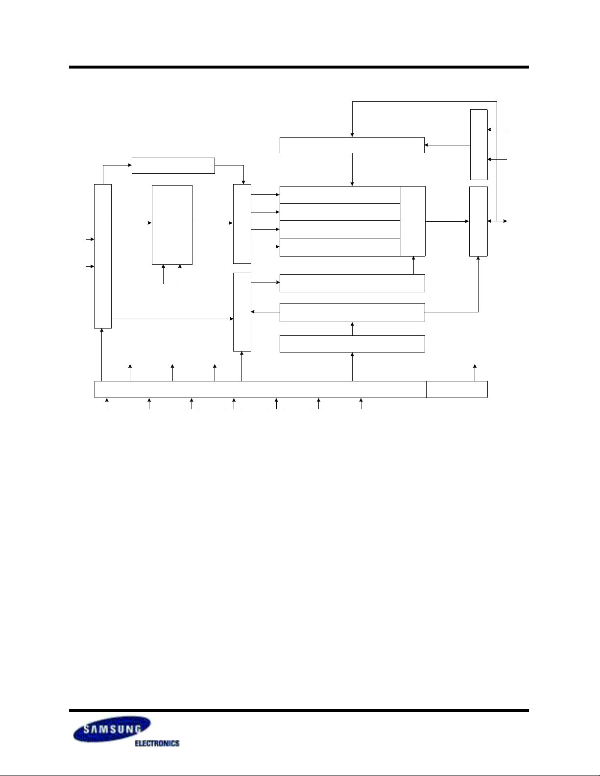
FUNCTIONAL BLOCK DIAGRAM
Bank Select
Mobile-SDRAM
LWE
Data Input Register
LDQM
CLK
ADD
LCKE
Refresh Counter
Row Buffer
Address Register
LRAS
LCBR
LRAS LCBR LWE LDQM
CLK CKE CS
Row Decoder Col. Buffer
LCAS LWCBR
Timing Register
RAS CAS WE L(U)DQM
1M x 16
1M x 16
1M x 16
1M x 16
Column Decoder
Latency & Burst Length
Programming Register
Sense AMP
Output BufferI/O Control
DQi
February 2004
K4S641633H - R(B)E/N/G/C/L/F
Package Dimension and Pin Configuration
E
1
Mobile-SDRAM
< Top View
*2
>< Bottom View*1 >
521634897
A
B
C
D
1
D
E
F
G
H
J
E
E/2
e
D
D/2
*2: Top V iew
A
A1
z
b
*1: Bottom View
< Top View*2 >
#A1 Ball Origin Indicator
K4S641633H
SEC Week
XXXX
123789
A VSS DQ15 VSSQ VDDQ DQ0 VDD
B DQ14 DQ13 VDDQ VSSQ DQ2 DQ1
C DQ12 DQ11 VSSQ VDDQ DQ4 DQ3
D DQ10 DQ9 VDDQ VSSQ DQ6 DQ5
E DQ8 NC VSS VDD LDQM DQ7
F UDQM CLK CKE CAS
G NC A11 A9 BA0 BA1 CS
HA8A7A6A0A1A10
J VSS A5 A4 A3 A2 VDD
Pin Name Pin Function
CLK System Clock
CS
CKE Clock Enable
A
0 ~ A11 Address
BA
0 ~ BA1 Bank Select Address
RAS
CAS
WE
L(U)DQM Data Input/Output Mask
0 ~ 15 Data Input/Output
DQ
V
DD/VSS Power Supply/Ground
V
DDQ/VSSQ Data Output Power/Ground
Symbol Min Typ Max
A 0.80 0.90 1.00
A
1
E - 8.00 -
E
1
D - 8.00 -
D
1
e - 0.80 b 0.40 0.45 0.50
z--0.10
54Ball(6x9) FBGA
RAS WE
Chip Select
Row Address Strobe
Column Address Strobe
Write Enable
[Unit:mm]
0.27 0.32 0.37
-6.40-
-6.40-
February 2004
K4S641633H - R(B)E/N/G/C/L/F
Mobile-SDRAM
ABSOLUTE MAXIMUM RATINGS
Parameter Symbol Value Unit
Voltage on any pin relative to V
Voltage on V
DD supply relative to Vss VDD, VDDQ -1.0 ~ 4.6 V
ss VIN, VOUT -1.0 ~ 4.6 V
Storage temperature T
Power dissipation P
Short circuit current I
NOTES:
Permanent device damage may occur if ABSOLUTE MAXIMUM RATINGS are exceeded.
Functional operation should be restricted to recommended operating condition.
Exposure to higher than recommended voltage for extended periods of time could affect device reliability.
STG -55 ~ +150 °C
D 1.0 W
OS 50 mA
DC OPERATING CONDITIONS
Recommended operating conditions (Voltage referenced to VSS = 0V, TA = -25 to 85°C for Extended, -25 to 70°C for Commercial)
Parameter Symbol Min Typ Max Unit Note
Supply voltage
Input logic high voltage VIH 2.2 3.0 VDDQ + 0.3 V 1
Input logic low voltage VIL -0.3 0 0.5 V 2
Output logic high voltage VOH 2.4 - - V IOH = -0.1mA
Output logic low voltage VOL - - 0.4 V IOL = 0.1mA
Input leakage current ILI -10 - 10 uA 3
NOTES :
1. VIH (max) = 5.3V AC.The overshoot voltage duration is ≤ 3ns.
2. VIL (min) = -2.0V AC. The undershoot voltage duration is ≤ 3ns.
3. Any input 0V ≤ VIN ≤ VDDQ.
Input leakage currents include Hi-Z output leakage for all bi-directional buffers with tri-state outputs.
4. Dout is disabled, 0V ≤ VOUT ≤ VDDQ.
VDD 2.7 3.0 3.6 V
VDDQ 2.7 3.0 3.6 V
CAPACITANCE (VDD = 3.0V & 3.3V, TA = 23°C, f = 1MHz, VREF =0.9V ± 50 mV)
Pin Symbol Min Max Unit Note
Clock CCLK 2.0 4.0 pF
RAS, CAS, WE, CS, CKE, DQM CIN 2.0 4.0 pF
Address CADD 2.0 4.0 pF
DQ0 ~ DQ15 COUT 3.5 6.0 pF
February 2004
 Loading...