

Samsung K4S641632H-TC60, K4S641632H-TL75, K4S641632H-TL70, K4S641632H-TC75, K4S640832H-TL75 Datasheet
...
SDRAM 64Mb H-die (x4, x8, x16)
64Mb H-die SDRAM Specification
CMOS SDRAM
Revision 1.4
November 2003
* Samsung Electronics reserves the right to change products or specification without notice.
Rev. 1.4 November 2003
SDRAM 64Mb H-die (x4, x8, x16)
Revision History
CMOS SDRAM
Revision 0.0 (May, 2003)
• Target spec release
Revision 0.1 (July, 2003)
• Preliminary spec release
Revision 0.2 (August, 2003)
• Modified IBIS characteristic.
Revision 1.0 (September, 2003)
• Finalized
Revision 1.1 (September, 2003)
• Corrected IBIS Specification.
Revision 1.2 (October, 2003)
• Deleted speed 7C at x4/x8.
Revision 1.3 (October, 2003)
• Deleted AC parameter notes 5.
Revision 1.4 (November, 2003)
• Modified Pin Function description.
Rev. 1.4 November 2003
SDRAM 64Mb H-die (x4, x8, x16)
CMOS SDRAM
4M x 4Bit x 4 / 2M x 8Bit x 4 / 1M x 16Bit x 4 Banks Synchronous DRAM
FEATURES
• JEDEC standard 3.3V power supply
• LVTTL compatible with multiplexed address
• Four banks operation
• MRS cycle with address key programs
-. CAS latency (2 & 3)
-. Burst length (1, 2, 4, 8 & Full page)
-. Burst type (Sequential & Interleave)
• All inputs are sampled at the positive going edge of the system
clock
• Burst read single-bit write operation
• DQM (x4,x8) & L(U)DQM (x16) for masking
• Auto & self refresh
• 64ms refresh period (4K cycle)
GENERAL DESCRIPTION
The K4S640432H / K4S640832H / K4S641632H is 67,108,864 bits synchronous high data rate Dynamic RAM organized as 4 x
4,194,304 words by 4 bits, / 4 x 2,097,152 words by 8 bits, / 4 x 1,048,576 words by 16 bits, fabricated with SAMSUNG′s high performance CMOS technology. Synchronous design allows precise cycle control with the use of system clock I/O transactions are possible
on every clock cycle. Range of operating frequencies, programmable burst length and programmable latencies allow the same device to
be useful for a variety of high bandwidth, high performance memory system applications.
Ordering Information
Part No. Orgainization Max Freq. Interface Package
K4S640432H-TC(L)75 16Mb x 4 133MHz(CL=3)
K4S640832H-TC(L)75 8Mb x 8 133MHz(CL=3)
K4S641632H-TC(L)60
K4S641632H-TC(L)70 143MHz(CL=3)
K4S641632H-TC(L)75 133MHz(CL=3)
4Mb x 16
166MHz(CL=3)
LVTTL 54pin TSOP(II)
Rev. 1.4 November 2003
SDRAM 64Mb H-die (x4, x8, x16)
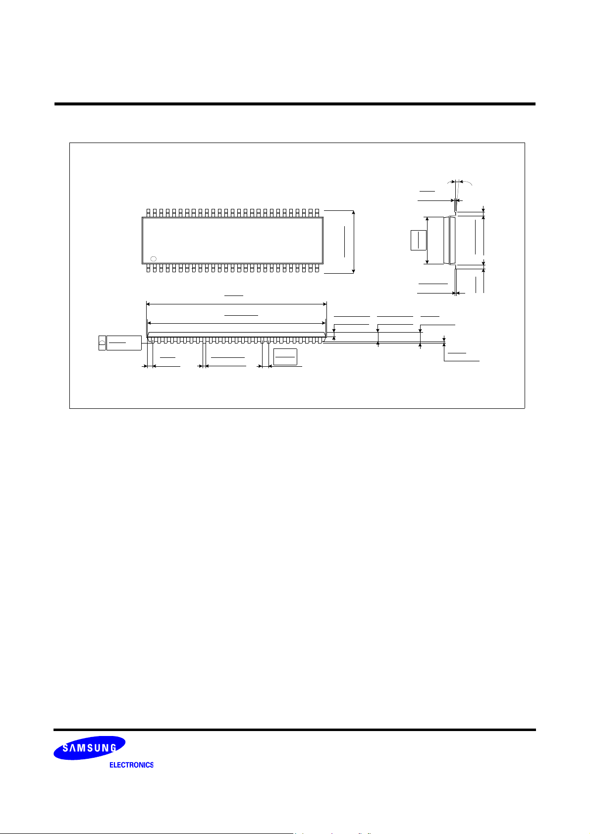
Package Physical Dimension
CMOS SDRAM
0.10
0.004
MAX
#54
#1
0.71
( )
0.028
#28
11.76±0.20
0.463±0.008
#27
22.62
MAX
0.891
22.22
0.30
0.012
0.875
+0.10
-0.05
+0.004
-0.002
± 0.10
± 0.004
0.80
0.0315
0.21
0.008
± 0.05
± 0.002
54Pin TSOP(II) Package Dimension
1.00
0.039
± 0.10
± 0.004
0.25
0.010
10.16
0.125
0.005
0.047
0.400
1.20
TYP
+0.075
-0.035
+0.003
-0.001
MAX
0.05
0.002
0~8°C
0.45~0.75
0.50
MIN
0.018~0.030
)
0.020
(
Rev. 1.4 November 2003
SDRAM 64Mb H-die (x4, x8, x16)
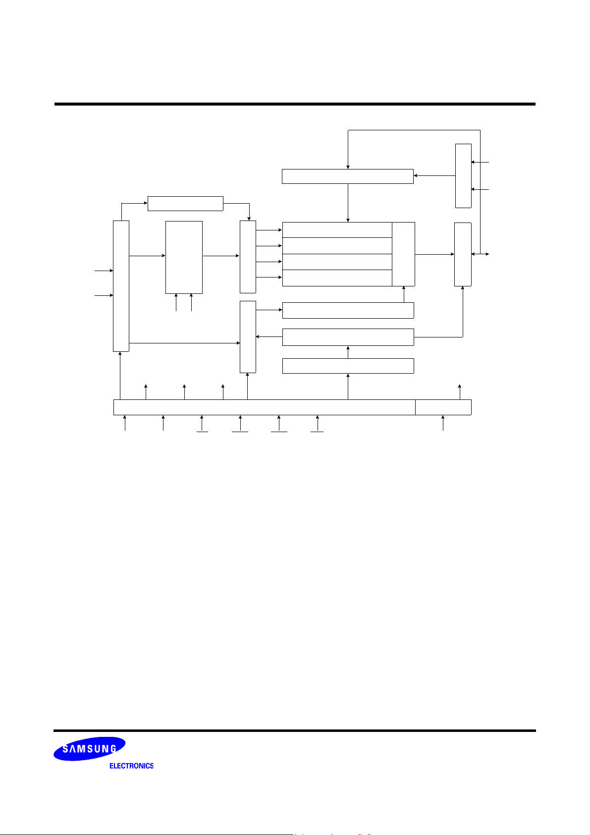
FUNCTIONAL BLOCK DIAGRAM
Bank Select
CMOS SDRAM
LWE
Data Input Register
LDQM
CLK
ADD
Refresh Counter
Row Buffer
Address Register
LRAS
LCBR
LCKE
LRAS LCBR LWE LDQM
CLK CKE CS
Samsung Electronics reserves the right to change products or specification without notice.
*
Row Decoder Col. Buffer
LCAS LWCBR
Timing Register
RAS CAS WE L(U)DQM
4M x 4 / 2M x 8 / 1M x 16
4M x 4 / 2M x 8 / 1M x 16
4M x 4 / 2M x 8 / 1M x 16
4M x 4 / 2M x 8 / 1M x 16
Column Decoder
Latency & Burst Length
Programming Register
Sense AMP
Output BufferI/O Control
DQi
Rev. 1.4 November 2003
 Loading...