

Samsung SM-G531F, Galaxy Grand Prime 4G Schematics TSHOO
8. Level 3 Repair
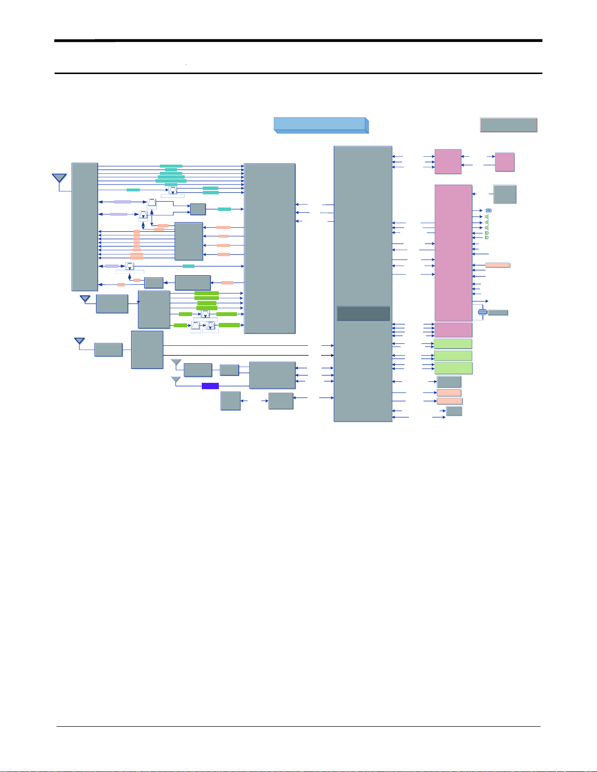
8-1. Block Diagram
(VIETMOBILE.VN)
FEM I D
LMSWK DGP- G55
LTE_B28_TRx_A
LTE_B28_TRx_B
LTE_B7_TRx
B40_Tx
Diversity LNA
SFMR3L0K001
SFMG2XAB002
LTE_B40_Rx
GSM_ HB_ Tx
GSM_LB_ Tx
SAYFH2G53CC0F0AR05
B8532
B1_Tx
B2_Tx
B3_Tx
B5_Tx
B8_Tx
B20_Tx
B7_Tx
Diversity FEM
SFMR6D0K001
GPS
88L200R
LTE_WCDMA_B1_Rx
LTE_WCDMA_B5_Rx
WCDMA_B2_GSMHB_Rx
LTE_W CD M A_B 8 _ GSM LB_Rx
B8531
B28_A_Tx
B28_B_Tx
SW
BGS12PL6
LTE_B3_Rx
LTE_B20_Rx
SAFFB2G35FB0F3K
MMMB
SKY77621
LTE_B7_Rx
LTE B7 / 0 PA
SKY77778
DRX_B40
DRX_B2 8
SAFEA2G45MB0F3K
LTE_B40_Rx_P
LTE_B40_Rx_N
SW
RF1624
DRX_B1_B3_P/N
DRX_B5_B8_P/N
DRX_B7_P/N
DRX_B20_ P/ N
SAFFB2G35FB0F3K
HHM1942A3
B8323
FILTER
FM AN T
LTE_B28_Rx
B1/B2/ B3_Tx
B5/ B8_ Tx
GSM_HB_ Tx
GSM_LB_ Tx
B7_B40_Tx
DRX_B40_ P/ N
DRX_B4 0_P/ N
SW
RDA SW2 5
BATT
2600mA
RF P A RT
TRANSCEIV ER
88RF858
BT/WIFI/FM
88W8777
NFC_ANT
NFC
S3F W RN5
SM - G 5 3 1 F
DIGRF_EN
RF_RST
TX_DI GRF_D_ P/ N
GLN_P/ N
GPS_P/ N
FM_ DA TA
BT_DATA
WLAN_DATA
NFC_I2C
PXA1908
1.2GHz Quad
Cort ex-A53
512KB L2 Cach
6Gb LPDDR3 @2 00M Hz
MUIC_I2C/ INT
USB_AP_D_P/N
UART_T/ RXD
VBUS_SW
PMIC_INT_N
PMIC_RST_OUT_N
I2S_D_IN/OUT
I2S_BCK
VCXO_EN
PMU_I2C_1P8
DVC1/ 2/ 3
DDR3_CA0:9
DDR_DQ0:3 1
EMMC_D0:7
DATA/CLK/CMD
MIPI_4Lane
AF/EEP/ CAM I2C
MIPI 2 lane
VTCAM I 2C
MIPI_3LANE
TSP_I2C/ IN T
SENSOR _ I 2 C / I NT
MOTOR_EN
VOL_UP/DN
SIM _ R ST/ Cl K / D A T/ D ET
T_FLASH_D0:3
MUIC
SM5504
PM I C
88PM886
6Gb+4GB eMCP
8M M AIN CAM
5M CAM
5" WXGA LCD
+ TSP
ACCEL
(K2HHTR)
MOTOR
VOL U M E K EY
SI M
Confidential
USB_D_P/N
USB_ID
BATT_I D
EAR_ADC_3.5
EAR _ M I C_ DET
JIG_ON_N From MUI C
MAIN_THM
PA_ THERM 0
AP_THERM
IF CONN
BATT
2600mA
LED
SPK
RCV
EAR _SP K
MAIN MIC
EAR M I C
HPGND
POW ER KEY
VOL_DN
RFCLK1_19.2M
(TO WTR1605L)
32.768KHz
8-1
Confidential and proprietary-the contents in this service guide subject to change without prior notice.
Distribution, transmission, or infringement of any content or data from this document without Samsung’s written authorization is strictly prohibited.
Level 3 Repair
(VIETMOBILE.VN)
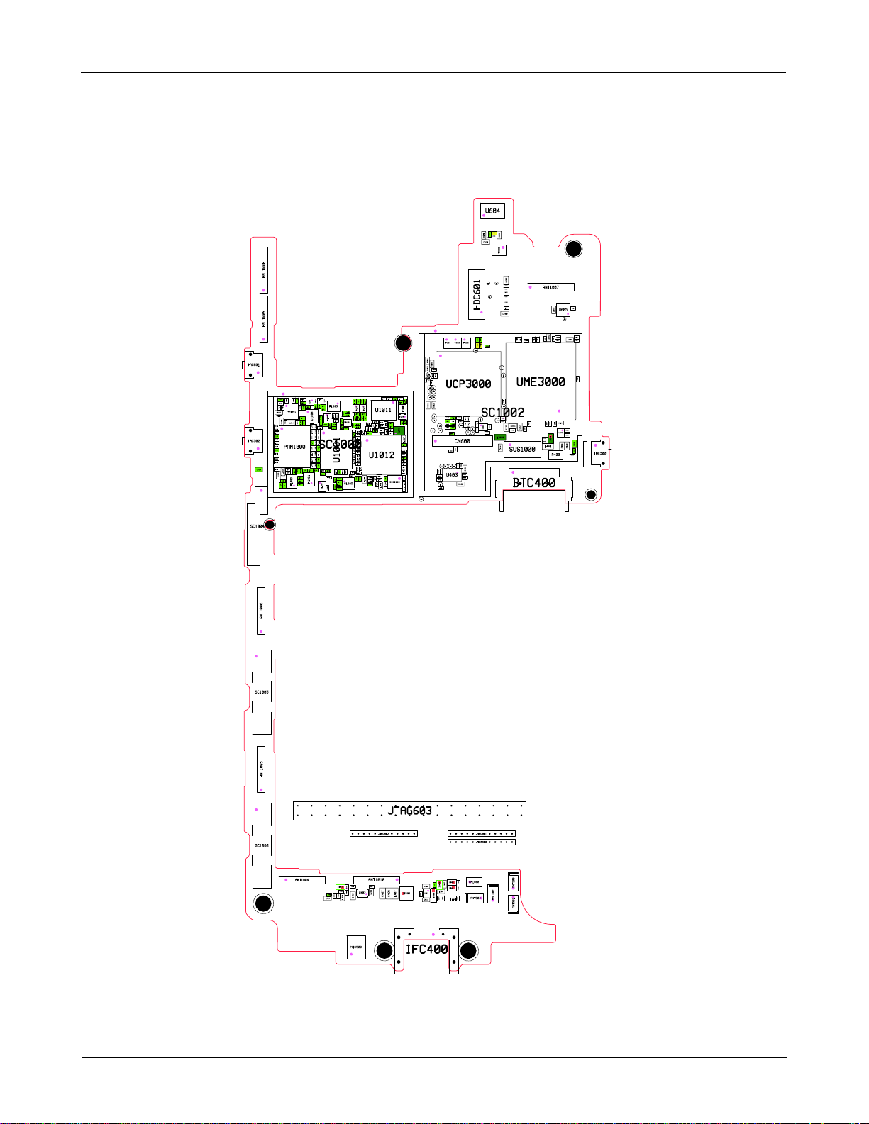
8-2. PCB Diagrams
8-2-1. Top
U604
R618
C634
R620
C637
C636
C635
TR500
BH400
TAC501
TAC502
SC1004
ANT1008ANT1009
R3034
R3035
C3028
R3036
TP_RF_CONT[3000
U3001
C3044
C3046
TP_TEST_PIN_PLLM
TP_PA_MODE
C3049
TP1000
UCP3000
TP1002
TP1001
TP1003
TP_TX_DIGRF_D_NTP_TX_DIGRF_D_P
R3033
R3032
TP202
R3020
TP200
R3024
R3023
TP402
R3021
TP401
TP201
TP405
TP406
C471
R3002
U403
R3001
TP_EXTON_N
R408
TP_UB
F600F601 F602
R3016
R3019
R3018
R3017
R602
CN600
C226
TP403TP404
R3008
R3007
TP_JTAG_SEL
R203
C472
R402
C465
C470
C469
BH406
C1117
C1126
L1072
C533
C1075
L1055
C1082
C1083
C1081
L1109
C1092
C1070
L1029
U1006
L1052
F1003
C1143
L1048
C1144
C1076
C1090
C1089
C1102
L1061
PAM1001
C1077
C1084
C1014
C1004
C1003
R1001
C1035
L1027
C1002
C1005
L1002
C1017
PAM1000
C1027
L1011
C1019
C1008
C1021
C1007
C536
L1042
C1006
L1062
C1025
L1047
F1002
C1058
C1060
C1049
L1028
U1004
L1037
C1044
C1015
C1037
C1039
L1060
C1146
L1110
C1114
L1069
L1093
L1046
C1061
C1062
C1047
C1029
SC1000
L1057
C1024
C1055
C1028
L1019
L1111 L1112
L1004
C1032
C1033
C1040
C1141
L1032
L1039L1040
C1045
L1005
L1043
C1053
C1020
C1052
L1036
F1001
C1051
CPL1000
C1111
L1051
F1004
L1050
L1108
L1059
L1049
U1001
L1008
L1107
C1022
C1001
C1065
C1064
C1063
L1044
C1059
L1045
R1000
L1076
L1077
L1074
C1116
F1006
C1048
L1070
C1043
C1042
L1071
L1073
L1024
F1000
L1023
C1057
L1017
L1021
C1036
L1033
L1038
L1034
L1006
L1007
L1012
L1000
L1001
L1003
L1053
L1054
L1056
L1013
L1015
U1012
L1016
L1020
L1022
L1025
L1026
L1031
C1038
L1010
C1026
L1030
C1041
C1054
C1056
U1005
L1103
C1145
F1007
F1008
U1011
L1075
F1009
C1123 C1124
C1125
L1078
L1083
L1104
L1105
C1133
L1087
L1085
L1086
C1134
L1079
L1081
C1132
L1088
L1089
L1092
L1082
L1091
U1003
C1130
L1099
L1035
L1090
L1113
C1112
C1080
C1095
C1103
C1113
C1096
C1120
C1079
L1094
C1087
C1109
C1069
C1072
C1086
C1104
C1108
R1003
OSC1000
L1106
C1107
C1066
C1085
L1058
C1071
TP_600
TP603
TP602
HDC601
C600
C609
R608
R606
C630
TP_GPS_CLK_N
SC1002
TP3000
R3022
R3025
TP_EMMC_CLK
C3019
R3011
R3012
C3020
SLEEP_IND
U3000
TP_SYS_CLK_EN
R3026
TP_ANT_SW3000
TP_RST
R3027
L3000
C466
C606
R605
ANT1007
R604
R603
C607
C605
L600
C608
C3010
C3011
C3018
R3013
R3000
TP_DDR_CA3000
TP_DDR_DQ3000
UME3000
R3028
TP_DOWNLOAD_MODE
VR402
C457
C3016
C3014
C437
C432
C429
C3015
C444
SUS1000
BTC400
C639
U605
C640
TP_ACC_INT
R3038
R3003
C3001
R3029
C3000
C3002
R3004
R3037
C3064
C3012
C3013
R3014
R3015
C259
U205
C260
C462
VR400
R404
C526
L408
C449
C464
C527
TAC500
C463
R400
BH405
BH401
SC1005
ANT1005 ANT1006
JTAG603
JTAG601JTAG602
SC1006
ANT1004
BH402
ANT1010
C532
R403
ZD512
VR401
C530
U402
C456
C528
L512
C458
C474
C531
C459
L514
MIC500
BH403 BH404
ZD403
L407
C467
C468
IFC400
C506
U501
R503
C511
JTAG600
ZD402
GA1000
R405R406
C473
R407
ZD400
ZD401
L500
D500
ANT503
C502
C535
C504
L515
ANT500ANT501
ANT502
8-2
Confidential and proprietary-the contents in this service guide subject to change without prior notice.
Distribution, transmission, or infringement of any content or data from this document without Samsung’s written authorization is strictly prohibited.
(VIETMOBILE.VN)
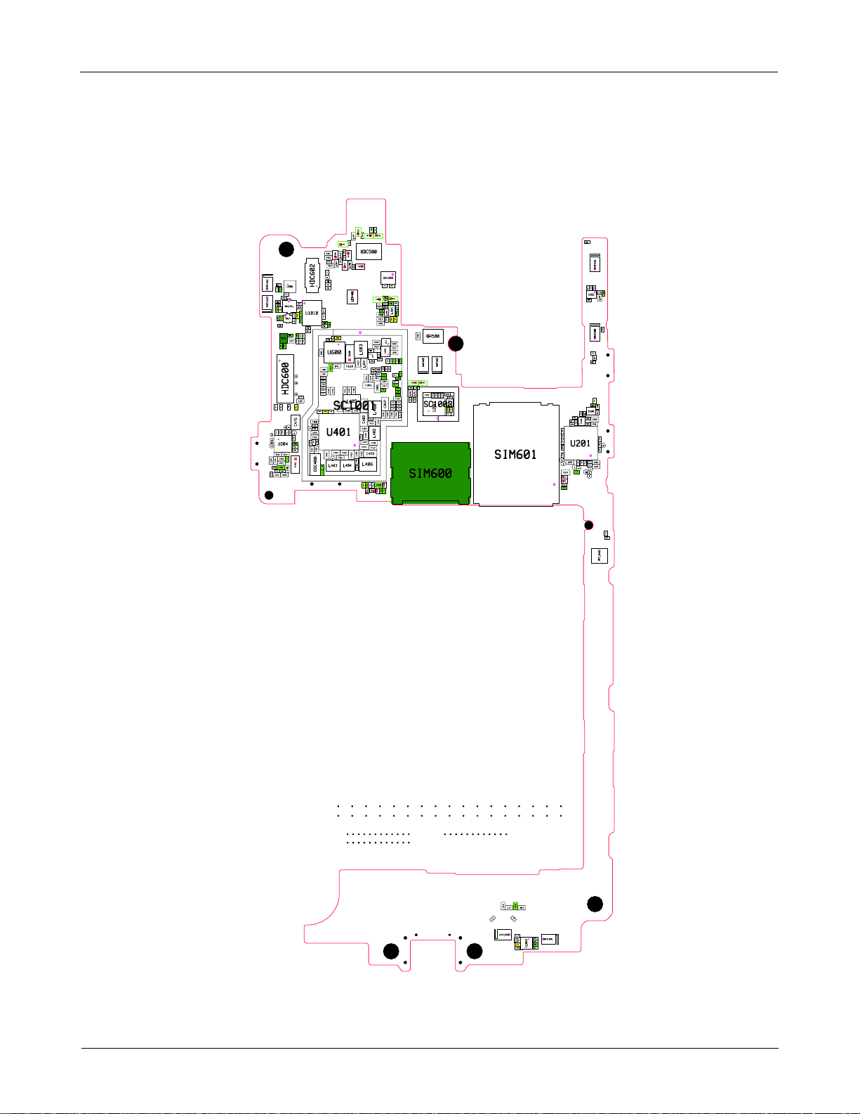
8-2-2. Bottom
Level 3 Repair
C507
C508
ZD510
ZD500ZD501
R511
L507
R514
ZD509
HDC500
C523
L511
L510
ZD508
ZD505
R515
C525
R516
C522
L509
R513
ZD506
L508
ZD507
C524
R607
TP604
C611
L1065
ANT1002ANT1003
C1099
C1105
C1098
L1101
C1128
RFS1001
C1129
C1140
L1080
C1127
L1084
TR600
R624
HDC600
R521
R522
C244
C245
C256
TP204 TP205
TP_NFC_EN
U204
TP_NFC_IRQ
L212L213
C250
C253
C254
C251
C255
C252
C460C461
C247
C246
R205
C612
HDC602
U606
C613
C643
C1097
L1063
L1064
U1010
C1121C1122
R1005
C1131C1135
C1106
U1013
C1118
C1119
C1115
C1110
L1066
R622
R600
R601
C601
R610
R611
R621
C443
C602
C603
C604
R623
U600
R609
L601
C644
C3006
C3007
TP600
C3003
C3009
TP601
C3008
C3005
C3004
C440
C442
C3063
TP_ERR
C407
C415
R517
R518
C476
TP_NFC_TCK
TP203
R206
R207
TP206
C243
C258
C257
C242
C249
D401
C248
SC1001
C426
C451
R520
C418
C417
TP407
C411
C420
U401
C419
C408
C409
C446
C427
C450
C404
C424
TP400
L403 L404
OSC400
C447 C448
C410
C414
OSC200
C237
C240
C521
ZD504
ZD511
C520
LED400
C518
C537
C534
C475
C529
L513
L504
R512
L505
R505
L506
R508
C519
R507
R509
R510
R506
C633
C619
C1101
L603
C1100
D600
U1007
R1002
C3048
C614
L602
C610
C3038
C3041
C3040
C3039
C3042
R3031
R3030
C3021
C3031
C438
C439
C441
L405
C422
C421
C406
L400
C401
C402
C412
C431
C403
L402
C425
C445
C452
C430
C454
C413
C405
C455
C453
C400
C423
C428
L406
C416
C628
C631
R613
R614
R617
ZD606
ZD604
ZD605
U603
C632
C617
C620
U602
C3051
C3052
C3053
C3055
C3058
C3061
C3059
C3026 C3027
C3032 C3033
C3024
C3036
C3034
C3035
C3025
C3023
C3029
C3022
C3030
C3057
C3062
C3043 C3045
C3037
C3056
C3060
C433
C434
C435
C436
SIM600
ZD601
C621
R615
C3050
C3054
C3047
GA500
C505
ANT505
ZD502 ZD503
C516 C517
L502
L501
C514
C515
SC1003
ANT504
L208
C229
C232
C233
C230
C231
L210
F201
C236
C234
U203
R204
SIM601
C212 C2 13C214
U201
L200
C202
TP_WLAN_CLK_EN
L205
TP_PCM_RXD
C629
ZD602
ZD600
C622
R612
L214
L209
L211
C235
C241
C238
U202
L207
L206
C210
ANT200 ANT201
C216
L216
L217
C261
L202
C208
F200
L201
C209
L215
C221
C222
C200
L204
U200
C220
C224
C201
L203
C206
TP_PCM_TXD
C215
C262
R200
C203
C204
C219
C211
R202
C205
TP3001
TP_PCM_SYNC
TP_WLAN_DAT_202
TP_WLAN_DAT_200
C263
TP_WLAN_DAT_203
TP_WLAN_DAT_201
C1011
L1009
RFS1000
C1013
C1012
C1010
C1142
L1067
L1068
ANT1000
C1136
L1041
ANT1001
C1046
L1096
C1137
C1050
R1004
U1002
L1095
C1138
8-3
Confidential and proprietary-the contents in this service guide subject to change without prior notice.
Distribution, transmission, or infringement of any content or data from this document without Samsung’s written authorization is strictly prohibited.

Level 3 Repair
8-3. Flow Chart of Troubleshooting
Equipments
Oscilloscope
Power Supply
Digital Multimeter
+ driver, ESD Safe Tweezer
8960 & Spectrum Analyzer
8-4
Confidential and proprietary-the contents in this service guide subject to change without prior notice.
Distribution, transmission, or infringement of any content or data from this document without Samsung’s written authorization is strictly prohibited.
Soldering iron
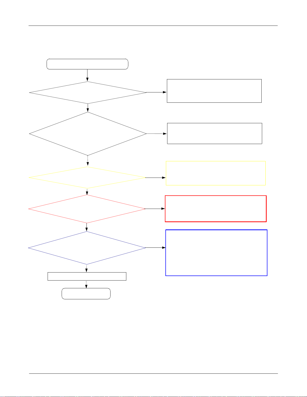
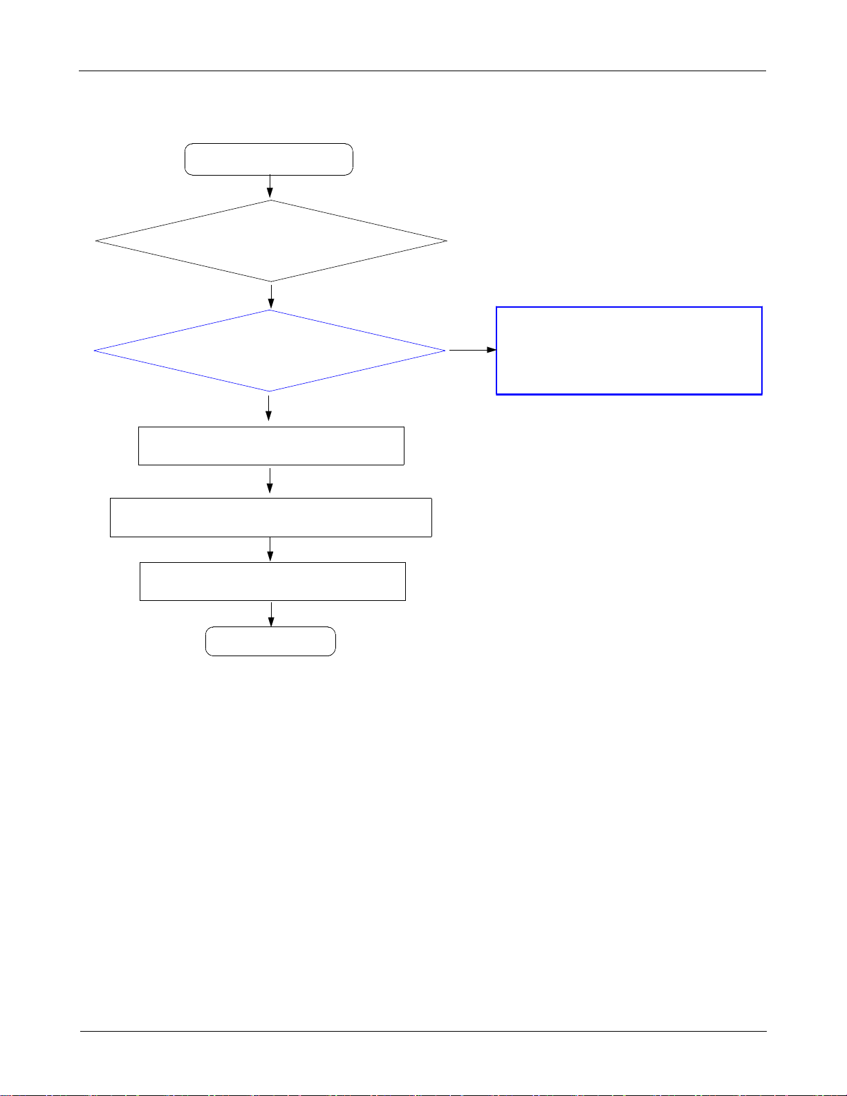
8-3-1. Power On
Mobile phone does not power on.
Level 3 Repair
Check the Battery Voltage.
Is it more than 3.8V?
Yes
Power-on the phone and
check the power-on sound
or motor Vibration.
No
Check the PWR_KEY
(soldering crack, open, etc)
Yes
Check the C401, C402, C403,
C404, C405, C406,
L400, L402, L403, L404. L405
Yes
Check the Clock OSC400
Is that frequency 32.768Khz?
No
Yes
Abnormal
No
No
Charging the battery by TA.
If its voltage level is extremely low(under 3.0V),
Change the battery.
Change the FRONT-LCD ASSY
Check TAC500
(Damaged or not)
If the output voltage is not satisfied with normal
condition, Replace U401
or find the de-cap related power
Each voltage level has ±10% margin.
※
Change the OSC4000
If OSC4000 does not still work, Change the U4000
This problem is internal oscillator of U4000
Test condition (Oscilloscope setting)
Yes
check the initial operation
Yes
END
※
: 20.0us.div (time division)
8-5
Confidential and proprietary-the contents in this service guide subject to change without prior notice.
Distribution, transmission, or infringement of any content or data from this document without Samsung’s written authorization is strictly prohibited.

Level 3 Repair
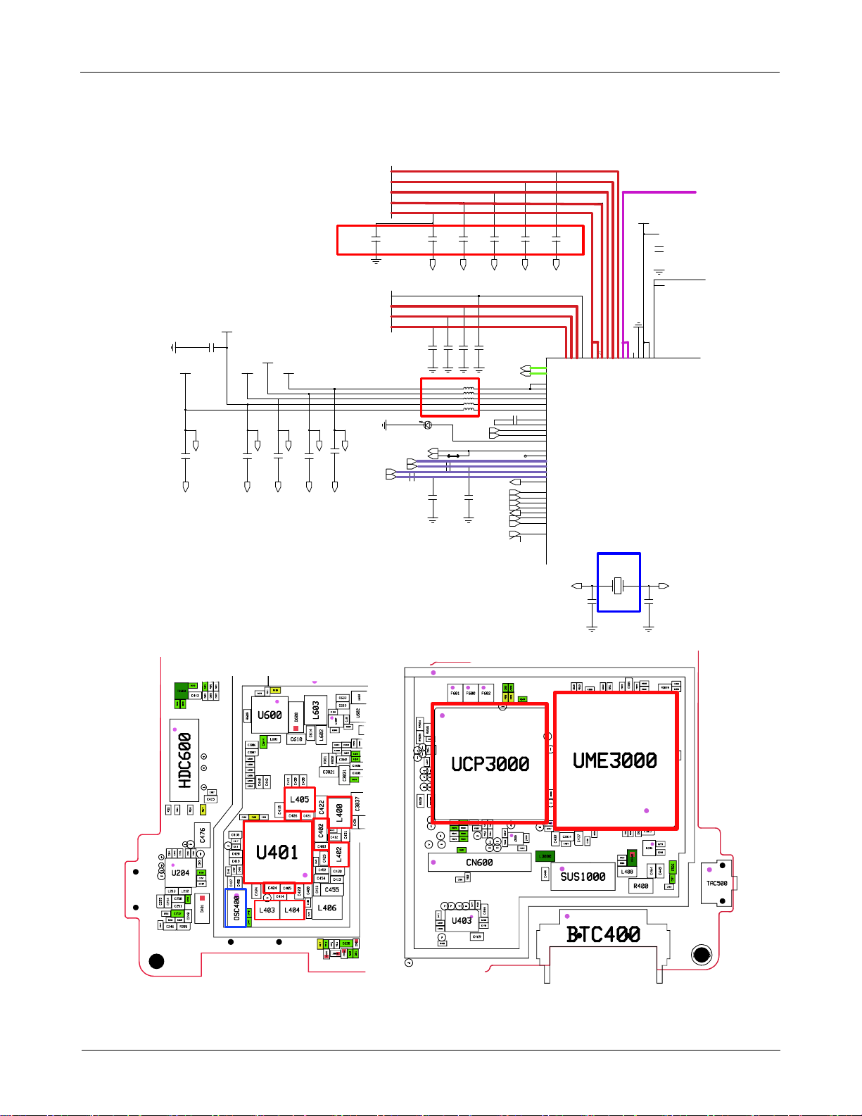
VREG_S5
APT_VOUT
C421
GND _S5
VRF_BUCK_1P8
C416
VSENSE_S5
TAC500
VREG_S3
C423
VREG_S2_1P8
1.2V
VSENSE_S4
GND _S4
7
VREG_S1
C424
GND _S3
Vcore 1.2V
VSENSE_S3
12
3456
VR EG _IN_S 5
VR EG _IN_S 4
VR EG _IN_S 3
VR EG _IN_S 2
VR EG _IN_S 1
C403
LED400
PMIC_CLK_32K
W LAN_SLEEP_CLK_32K
MAIN_MIC_N
MAIN_MIC_P
C475
C402
GND _S1
GND _S2
C414
C412
C413
L400
L402
L403
L404
L405
FLASH_EN
C474
C451
C401 C406
VREG_IN_L4
VREG_IN_L3
VREG_IN_L2
VREG_IN_L1
C422
C425
GND _S2
EA R_M IC_N
VSENSE_S1
VSENSE_S2
EAR_MIC_P
GND _S1
PA_EN
C426
C404
C415
EAR_G_DET
SPK_OUT_N
SPK_OUT_P
I2S_BCLK
VOL_DN
GPIO5V_1
APT_CTL0
I2S_D _IN
I2S_D _OU T
C405
GND _S3
GND _S4
GND _S5
J2
J8
G3
E9
D10
SPKN
SPKP
VX1
VX1
VX2
VX3
VX4
VX5
CFNLV
CFPLV
CF_EN
CF_MASK
CF_OUT
CLK32K1
CLK32K2
MICCLK12
MICD AT12
MICCLK34
MICD AT34
BCLK
GPIO0
GPIO1|DVC3
GPIO5V_1
GPIO5V_2
GPIO2|RF
DVC1
DVC2
SDO
SDI
G8
VIN2
VIN3
VIN1
VIN4
N8
N6
L1
L2
H1
A8
A6
N4
G15
C420
H15
K6
J5
A4
K7
G13
TP407
M13
N14
N13
N12
K14
N11
N10
DVC3
DVC1
DVC2
K5
J7
J6
L14
M15
PHONE_ON_N
C527
C526
XO_OU T XO_IN
B7
N5
K2
A7
K1
VINB3
VINB5
VINB1
VINB4
VINB1J1VINB2
U401
OSC400
2
C447
B3
A3
VBUS
VBUS
1
VREG_S2_1P8
B4
B6
D14
VDD18
VBUS_SNS
VBUS _G ATE
C407
VBAT_SYS
N9
L15
H11
VDDIO
VDD18
VDD_SPK
100mA Low Noise
100mA Low Noise
100mA Low Noise
10mA Low Noise
C448
8-6
Confidential and proprietary-the contents in this service guide subject to change without prior notice.
Distribution, transmission, or infringement of any content or data from this document without Samsung’s written authorization is strictly prohibited.
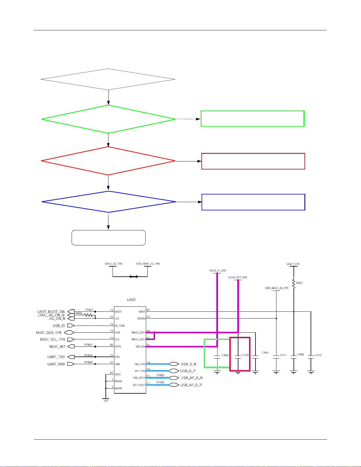
8-3-2. Initial
Level 3 Repair
Initial Failure
Yes
Re-download latest SW on the
Check the oscillator clock waveform.
Resoldering or Change UCP3000, U401, UME3000
mobile phone.
Abnormal
Check the Power On(8-3-1)
37.768KHz : OSC400
Normal
Try to boot recovety
Abnormal
Abnormal
Change PBA
Abnormal
Check the OSC400.
(Crack, open etc.)
Check the output clock waveforms and frequency.
Test condition (Oscilloscope setting)
※
: 20.0us.div (time division)
END
8-7
Confidential and proprietary-the contents in this service guide subject to change without prior notice.
Distribution, transmission, or infringement of any content or data from this document without Samsung’s written authorization is strictly prohibited.
Level 3 Repair
VREG_S5
C421
APT_VOUT
GND_S5
VRF_BUCK_1P8
C416
VSENSE_S5
VREG_S3
C423
VREG_S2_1P8
1.2V
VSENSE_S4
GND_S4
VREG_S1
C424
GND_S3
Vcore 1.2V
VSENSE_S3
VR EG _IN_S 5
VR EG _IN_S 4
VR EG _IN_S 3
VR EG _IN_S 2
VR EG _IN_S 1
C402
C401 C406
VR EG _IN_L4
VR EG _IN_L3
VR EG _IN_L2
VR EG _IN_L1
C403
GND _S1
C414
C412
C413
L400
L402
L403
L404
L405
LED400
PMIC_CLK_32K
W LAN _SLEEP _CLK_3 2K
C422
C425
VSENSE_S2
GND_S1
GND_S2
MAIN_MIC_N
MAIN_MIC_P
EA R_M IC_N
VSENSE_S1
EA R_M IC_P
C474
C475
C451
GND _S2
FLASH_EN
PA_EN
C426
C404
C415
EAR_G_DET
SPK_OUT_N
SPK_OUT_P
I2S_BCLK
VOL_DN
GPIO5V_1
APT_CTL0
I2S_D _IN
I2S_D_OU T
C405
GND _S5
GND _S4
GND _S3
J2
J8
G8
G3
N8
N6
L1
L2
H1
A8
A6
N4
G15
C420
H15
K6
J5
A4
K7
G13
TP407
M13
N14
N13
N12
K14
N11
N10
DVC3
DVC1
DVC2
E9
D10
K5
J7
J6
L14
M15
SPKN
SPKP
VX1
VX1
VX2
VX3
VX4
VX5
CFNLV
CFPLV
CF_EN
CF_MASK
CF_OUT
CLK32K1
CLK32K2
MICCLK12
MICDAT12
MICCLK34
MICDAT34
BCLK
GPIO0
GPIO1|DVC3
GPIO5V_1
GPIO5V_2
GPIO2|RF
DVC1
DVC2
SDO
SDI
VIN4
VIN2
VIN3
VIN1
J1
K1
N5
K2
A7
B7
VINB2
VINB1
VINB5
VINB1
VINB4
VINB3
U401
A3
B3
VBUS
VBUS
VREG_S2_1P8
B4
B6
D14
VDD18
VBUS_SNS
VBUS_G ATE
C407
VBAT_SYS
N9
L15
H11
VDDIO
VDD18
VDD_SPK
100mA Low Noise
100mA Low Noise
100mA Low Noise
10mA Low Noise
OSC400
XO_OUT XO_IN
2
1
C447
C448
8-8
Confidential and proprietary-the contents in this service guide subject to change without prior notice.
Distribution, transmission, or infringement of any content or data from this document without Samsung’s written authorization is strictly prohibited.
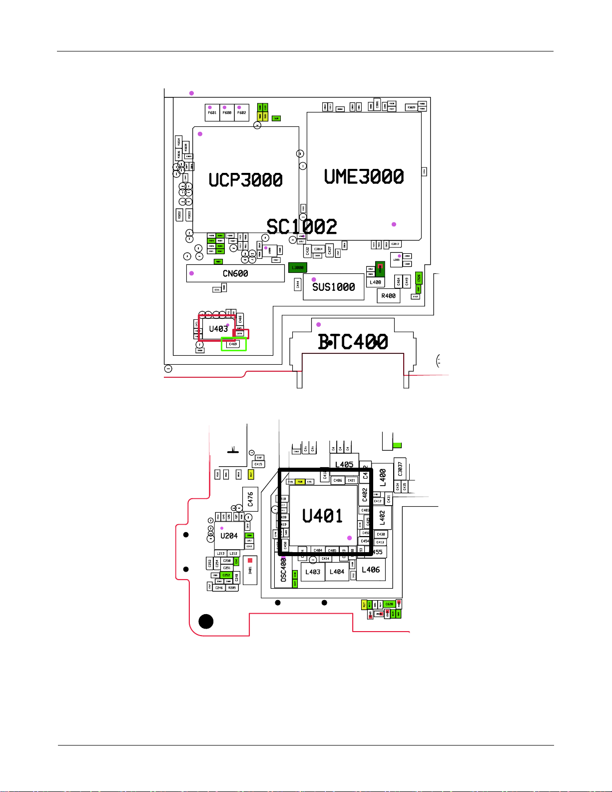
8-3-3. Charging Part
TA / USB Insert
Level 3 Repair
Yes
Charging Sequence Start
VBUS_5V_IF= 5V(C469)
Yes
Check the
VBUS_5V=5V(C470)
Yes
Battery is Charging?
Yes
END
No
No
No
Check the TA / USB connected or not
Resolder or Replace U403
Resolder or Replace U401
8-9
Confidential and proprietary-the contents in this service guide subject to change without prior notice.
Distribution, transmission, or infringement of any content or data from this document without Samsung’s written authorization is strictly prohibited.
Level 3 Repair
8-10
Confidential and proprietary-the contents in this service guide subject to change without prior notice.
Distribution, transmission, or infringement of any content or data from this document without Samsung’s written authorization is strictly prohibited.
 Loading...