

Samsung f300 Service Manual

GSM TELEPHONE
SGH-F300
GSM TELEPHONE
CONTENTS
Specification
1.
Exploded View and Parts list
2.
Chart of Troubleshooting
3.
Array course control
4.
Block Diagrams
5.
PCB Diagrams
6.
MAIN Electrical Parts List
7.
Reference data
8.
Safety Precautions
9.
Product Function
10.

Specification
1.
GSM General Specification
1-1.
GSM TX power class
1-2.
Exploded View and Parts list
2.
Cellular phone Exploded View
2-1.
Cellular phone Parts list
2-2.
Disassembly
2-3.
Assembly
2-4.
ChartofTroubleshooting
3.
Baseband
3-1.
...............................................................................................................2-9
..................................................................................................................2-11
............................................................................................................3-1
Contents
.......................................................................................1-1
...............................................................................................1-2
..................................................................................2-1
............................................................................................2-2
3-1-1.
3-1-2.
3-1-3.
3-1-4.
3-1-5.
3-1-6.
3-1-7.
3-1-8.
3-2.
3-2-1.
3-2-2.
3-2-3.
3-2-4.
3-2-4.
3-2-6.
Power ON
System Initial
SIM Part
Charging Part
Microphone Part
Speaker Part
Camera Part
LCD
.............................................................................................................3-21
RF
......................................................................................................................3-13
EGSM
DCS
PCS
EGSM
DCS
BLUETOOTH
Rx ......................................................................................................3-24
Rx ......................................................................................................3-25
&
.....................................................................................................3-1
................................................................................................3-5
.......................................................................................................3-8
.............................................................................................3-10
.........................................................................................3-12
..............................................................................................3-15
..............................................................................................3-18
Rx ...................................................................................................3-23
Tx ...................................................................................................3-27
PCS
Tx .........................................................................................3-28
..............................................................................................3-30

Array course control
4.
Downloading Binary Files
4-1.
Pre-requsite for Downloading
4-2.
S/W Downloader Program
4-3.
Block Diagrams
5.
PCB Diagrams
6.
MAIN Electrical Parts List
7.
Reference data
8.
Reference Abbreviate
8-1.
Contents
......................................................................................4-2
................................................................................4-2
.....................................................................................4-3
..............................................................................................8-1
Safety Precautions
9.
Repair Precaution
9-1.
ESD(Electrostaically Sensitive Devices) Precaution
9-2.
Product Function
10.
......................................................................................................9-1
................................................9-2
Specification
1.
GSM General Specification
1-1.
GSM 900
Freq. Band[MHz]
Uplink/Downlink
ARFCN range
Tx/Rx spacing 45 MHz 95 MHz 80 MHz
Mod. Bit
rate/
Bit Period
Time Slot Period/Frame
Period
Modulation
MS Power
GPRS
EDGE
GPRS 0.3 GMSK 0.3 GMSK 0.3 GMSK
EDGE 8 PSK 8 PSK 8 PSK
GPRS 33 dBm~5 dBm 30 dBm~0 dBm 30 dBm~0 dBm
EDGE 27~5 dBm 26~0 dBm 26~0 dBm
880~915
925~960
0~124
& 975~1023
270.833 Kbps
3.692 us
812.5 Kbps
3.692 us
576.9 us
4.615 ms
DCS1800 PCS1900
1710~1785
1805~1880
512~885 512~810
270.833 Kbps
3.692 us
812.5 Kbps
3.692 us
576.9 us
4.615 ms
1850~1910
1930~1990
270.833 Kbps
3.692 us
812.5 Kbps
3.692 us
576.9 us
4.615 ms
Power Level
Sensitivity -102 dBm -100 dBm -102 dBm
TDMA Mux 8 8 8
Cell Radius 35 Km 2 Km 2 Km
GPRS 5
EDGE 8~19(class E2) 2~15(
pcl~19 pcl
1-1
pcl~15 pcl
0
class E2)
pcl~15 pcl
0
2~15(
class E2)
Specification
GMSK TX power Level
1-2.
TX Power
control level
533±2
631±3
729±3
827±3
925±3
10 23±3
11 21±3
12 19±3
13 17±3
14 15±3
15 13±3
GSM900
dBm
dBm
dBm
dBm
dBm
dBm
dBm
dBm
dBm
dBm
dBm
TX Power
control
level
030±2
128±3
226±3
324±3
422±3
520±3
618±3
716±3
814±3
912±4
10 10±4
DCS1800
dBm
dBm
dBm
dBm
dBm
dBm
dBm
dBm
dBm
dBm
dBm
TX Power
control
level
030±2
128±3
226±3
324±3
422±3
520±3
618±3
716±3
814±3
912±4
10 10±4
PCS1900
dBm
dBm
dBm
dBm
dBm
dBm
dBm
dBm
dBm
dBm
dBm
16 11±5
17 9±5
18 7±5
19 5±5
dBm
dBm
dBm
dBm
11 8±4d
12 6±4
13 4±4
14 2±5
15 0±5
1-2
Bm
dBm
dBm
dBm
dBm
11 8±4
12 6±4
13 4±4
14 2±5
15 0±5
dBm
dBm
dBm
dBm
dBm
Specification
2-3.
EDGE TX Power Level
TX Power
control
level
827±3
925±3
10 23±3
11 21±3
12 19±3
13 17±3
14 15±3
15 13±3
16 11±5
GSM850
dBm
dBm
dBm
dBm
dBm
dBm
dBm
dBm
dBm
TX Power
control
level
226±3
324±3
422±3
520±3
618±3
716±3
814±3
912±4
10 10±4
DCS1800
dBm
dBm
dBm
dBm
dBm
dBm
dBm
dBm
dBm
TX Power
control
level
226±3
324±3
422±3
520±3
618±3
716±3
814±3
912±4
10 10±4
PCS1900
dBm
dBm
dBm
dBm
dBm
dBm
dBm
dBm
dBm
17 9±5
18 7±5
19 5±5
dBm
dBm
dBm
11 8±4
12 6±4
13 4±4
14 2±5
15 0±5
dBm
dBm
dBm
dBm
dBm
11 8±4
12 6±4
13 4±4
14 2±5
15 0±5
dBm
dBm
dBm
dBm
dBm
1-3

Exploded View and Parts List
2.
Cellular phone Exploded View
2-1.
QKP01
QME02
QMI03
QBA00
QMI01
QMI04
QRF01
QFR01
QLC01
QME01
QCA01
QMP01
QAN02
QSH01
QLC02
QMW01
QSD01
QRF03
QMC02
QSC05
QSC07
QMW02
QVK01
QBA01
QSC29
QBA02
QRE01
QCR70
QVO01
QCK02
QCK01
2-1
SAMSUNG Proprietary-Contents may change without notice
This Document can not be used without Samsung's authorization
QME03
QCK04
QCK03
QRE02
QVO08

Main Electrical Parts List
Cellular phone Parts list
2-2.
Design LOC Discription SEC CODE
QAN02 INTENNA-SGHF300 GH42-00997A
QBA01 SOFT BATTERY PACK-630MAH,BLK,E GH43-02620A
QBA02 INNER BATTERY PACK-950MAH,BLK, GH43-02792A
QCA01 UNIT-CAMERA MODULE GH59-03924A
QCK01 PMO-MODE KEY GH72-33514A
QCK02 ASSY KEY-HOLD GH98-03984A
QCK03 PMO-MP3 TOUCH KEY GH72-33520A
QCK04 PMO-OK KEY GSM GH72-34018A
QCR70 SCREW-TAPPING
6002-001402
QKP01 ASSY KEYPAD-(SER/ZKA) GH98-03827A
QLC01 LCD-MODULE SGHX510 GH07-00982A
QME01 UNIT-SPK/MOT ASS'Y GH59-03507A
QME03 UNIT-TOUCH KEY GH59-03506A
QMI03 RMO-RUBBER MIC GH73-08450A
QMI04 RMO-MIC HOLDER GH73-09225A
QMP01 PBA MAIN-SGHF300(PBA MAIN) GH92-03013A
QMW02 ASSY COVER-PHONE WINDOW GSM GH98-02161A
QRE01 MEA-REAR KIT GH97-07341A
QRE02 ASSY CASE-MP3 GH98-01986A
QRF01 PMO-RF COVER GH72-33879A
QSC05 RMO-RUBBER BATTERY
QSC07 RMO-RUBBER BATTERY
L
R
GH73-09007A
GH73-09008A
QSC29 RMO-RUBBER BATTERY GH73-08211A
QSH01 NDC-MAIN BRACKET GSM GH71-06802A
QVK01 UNIT-SIDE VOL KEY GH59-03525A
QVO01 ASSY KEY-VOLUME GH98-03985A
QVO08 NDC-SIDE BELT V2 GH71-06996A
QLC02 ELA UNIT-SGHF300 LCD MODULE GH96-02316A
QMW01 ASSY COVER-MAIN WINDOW GH98-02630A
QME02 UNIT-3X4 KEY GH59-03516A
QMI01 AS-MIC SVC GH81-05919A
QBA00 ASSY CASE-BATTERY TERMINAL GH98-03390A
QFR01 ASSY CASE-PHONE GH98-01980A
QMC02 PMO-COVER SIM GH72-33508A
QRF03 PMO-COVER EAR JACK GH72-33509A
QSD01 PMO-COVER SD GH72-33510A
2-2
SAMSUNG Proprietary-Contents may change without notice
This Document can not be used without Samsung's authorization

SEC CODE Discription
1109-001363
3719-001319
6902-000634
6902-000683
IC-MEMORY CARD
CONNECTOR-ADAPTOR
BAG PE
BAG ZIPPER
GH39-00686A CBF INTERFACE-MIC CABLE
GH39-00720A CBF INTERFACE-DLC,X830,BLK,PCB
GH44-01361A ADAPTOR-SGHE690,BLK,EU,A_TYPE
GH46-00399A S/W CD-SGHF300 PC STUDIO
3.1
GH59-03909A UNIT-EARPHONE,SGHF300,MAIN,PLU
GH68-04336A MANUAL-SFC
GH68-08494B LABEL(P)-BARCODE RUSSIA
GH68-09361A LABEL(R)-WATER SOAK
GH68-13514A MANUAL USERS-EU RUSSIAN
GH68-13668A LABEL(R)-MAIN
2
GH68-14730A MANUAL USERS-IMEI LEAFLET
GH69-04965A CUSHION-CASE TA2 MA2
GH69-04967B BOX(P)-UNIT MAIN SER
GH73-09011A RMO-RUBBER KEY FPCB
GH74-13804A MPR-REMOVE TAPE LCD
GH74-17600A MPR-INSU TAPE
GH74-17926A MPR-TAPE LED
GH74-20021A MPR-INSU TAPE
GH74-23391A MPR-INSU TAPE
GH74-26397A MPR-SPONGE PHONE LCD CONTACT
GH74-27919A MPR-SPONGE SPK MOTOR CONNECTOR
GH74-27921A MPR-SPONGE CAMERA CONNECTOR
GH74-28462A MPR-TAPE PBA SHEET
GH74-28463A MPR-TAPE PBA SHEET
GH74-28471A MPR-TAPE PBA SHEET
A
B
C
GH74-28891A MPR-TPAE PHONE LCD BACK
GH74-29280A MPR-INSU TAPE
GH74-29971A MPR-PBA SHEET
GH74-29972A MPR-PBA SHEET
D
G
GH74-29973A MPR-SPONGE
GH74-30411A MPR-INSU TAPE
GH74-30451A MPR-GASK TAPE
GH74-30452A MPR-GASK TAPE
Main Electrical Parts List
2-3
SAMSUNG Proprietary-Contents may change without notice
This Document can not be used without Samsung's authorization

Main Electrical Parts List
GH74-30453A MPR-GASK TAPE
GH74-30455A MPR-ELEC TAPE
GH74-30456A MPR-GASK TAPE
GH74-30457A MPR-GASK TAPE
GH74-30627A MPR-INSU TAPE PBA
GH74-30628A MPR-ELEC TAPE CAM
GH74-30630A MPR-INSU TAPE TOUCH KEY
GH74-30672A MPR-VINYL BOHO MP3
GH74-30673A MPR-VINYL BOHO MP3
GH74-30674A MPR-VINYL BOHO TOUCH
GH74-30675A MPR-VINYL BOHO PHONE
GH74-30676A MPR-VINYL BOHO PHONE
GH74-30768A MPR-VINYL BOHO TOUCH
GH74-30984A MPR-TAPE MP3 LCD
GH74-30985A MPR-TAPE MP3 LCD
GH74-31028A MPR-INSU TAPE
GH74-31188A MPR-VINYL BOHO MAIN WINDOW
GH74-31268A MPR-INSU TAPE
GH74-31473A MPR-GASK TAPE
GH74-31474A MPR-TAPE BATTERY CON BOTTOM
GH74-31495A MPR-GASK TAPE
GH74-31578A MPR-INSU TAPE
GH74-31579A MPR-GASK TAPE
GH74-31580A MPR-GASK TAPE
GH74-32171A TAPE GASK
A
B
B
A
B
A
A
B
2-4
SAMSUNG Proprietary-Contents may change without notice
This Document can not be used without Samsung's authorization
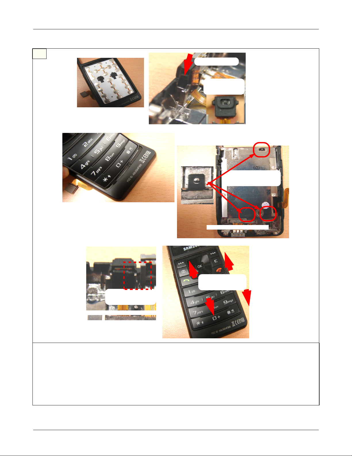
Disassembly
2-3.
1
Main Electrical Parts List
Adhere Window
Adhere Rubber
Adhere black tape
Adhere Sponge
Adhere conductive tape, adhesive tape and insulation tpae to the back side of LCD
1)
Adhereasponge to LCD connector
2)
Adherearubber below the LCD screen
3)
Adhereawindow up to the LCD
4)
Adhere an adhesive tape back of the MP3 LCD
5)
caution
※
Be care of scratch and molding damage.
1)
2
Down the
hold key
Assemble
hold key
Adhere adhesive tape
Adhere tape
Assemble Vol.
key
Assemble Mode
switch key
Adhere a
tape to fix
Inset the hold key, mode key and Vol. key into the side belt
1)
Adhereatape to fix the keys
2)
caution
※
Be care of scratch and molding damage.
1)
Especially FPCB of'con to con'
2-5
SAMSUNG Proprietary-Contents may change without notice
This Document can not be used without Samsung's authorization
Adhere a tape
to fix
Main Electrical Parts List
3
Insert the MIC.
Feature of MIC.
holder
Attach the key-PBA
Insert the MIC.
Hookthefringetothe
rib for fixing
Insert the Key-PAD
Press both side of
Key PAD
Attach the MIC
rubber
Attach the MIC rubber
Attach the Key PAD
Removeadetaching sheet of the Key-PBA
1)
Attach the Key-PBA to the Phone cover after inserting the connectors.
2)
Assemble the MIC. and MIC. holder
3)
Insert the MIC.
4)
AttachtheKeyPADandfixthefringeholetotherib
5)
caution
※
Be care of scratch and molding damage.
1)
Verify the direction of side key care of scratch and molding damage.
2)
Fixing fringe
2-6
SAMSUNG Proprietary-Contents may change without notice
This Document can not be used without Samsung's authorization
4
Main Electrical Parts List
①
③
tape A
Attach the tape 'ㄷ'
tape D
②
tape B
tape C
After setting tape and taping hole,
attach the tapes.
④
standard
line
tape E
Attach the tape by standizing
white line
⑤
(X)
(O)
Attach the tape by standizing red
Attach the tape
1)
Attach the tape B,C(rubber) at the lower part of MAIN keypad fringe.
2)
Attach an insulated tapeDat the lower part of within pnone cover.
3)
Attach the tapeEat inserting hole of pnone cover's key FPCB
4)
Attach an insulated tapeDat the upper part of MAIN keypad fringe.
5)
caution
※
Especially FPCB of'con to con'
1)
at inserting hole of pnone cover's key FPCB
'ㄷ'
tape F
line
.
.
2-7
SAMSUNG Proprietary-Contents may change without notice
This Document can not be used without Samsung's authorization

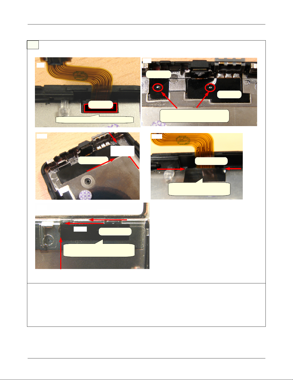
Main Electrical Parts List
5
③
①
①
EMI tape
<빨간색 실선을 기준으로
테이프를 부착한다>
도전 테이프 C
insert
camera
After attaching the tape by
<
standizing red line,
A
도전 테이프 B
④
②
removing the paper
Attach the tape by
<
standizing red line
remove papers of
both side tape
>
>
D
MOT and SPK
⑤
The real thing is no paper
<
>
insert the SPK
and MOT
Attach the EMI tapeAandBon EMI tape C.
1)
Attach the completed tape on camera.
2)
After attaching the tape on camera and removing the paper.
3)
Insert the camera in intenna.
4)
Remove the papers of MOT and SPK.
5)
Insert the MOT and SPK in intenna.
6)
caution
※
Be care of scratch and molding damage.
1)
Verify the direction of side key
2)
2-8
SAMSUNG Proprietary-Contents may change without notice
This Document can not be used without Samsung's authorization

6
Main Electrical Parts List
<Remove the paper> <Remove the paper> <Insert the key FPCB in MP3 cover>
<Attach the key FPCB on MP3 cover>
<Remove the paper>
<키 박리지 제거>
Attach the touch key pad
Remove the papers of touch key FPCB.
1)
Insert the touch key FPCB connector at MP3 cover.
2)
After setting between JIG's pin and hole's key PBA position by using the JIG, attaching the key PBA.
3)
Remove the paper of touch key FPCB.
4)
Attach the play key(
5)
Attach the touch key pad.(so as to the circle shape is positioned center)
6)
Attach the sponge on the upper side of touch key connector.
7)
caution
※
Be care of scratch and molding damage.
1)
▶Ⅱ
)ata
dome's center.
Attach the play key
<플레이 키 부착>
2-9
SAMSUNG Proprietary-Contents may change without notice
This Document can not be used without Samsung's authorization
Main Electrical Parts List
7
⑥
Assemble the lower end of front
small insulated tape
A
large insulated tape
A
Test of the sidebelt externally.
1)
Assemble the side belt and MP3 cover.
2)
the lower part of MP3 cover
=>
the left side ofalower part
→
Attachalarge insulated tape on the upper side of MP3 cover demper.
3)
Attachasmall insulated tape on the upper side of touch key chip.
4)
caution
※
Be care of scratch and molding damage.
1)
the right side ofaupper part
→
the left side ofaupper part
→
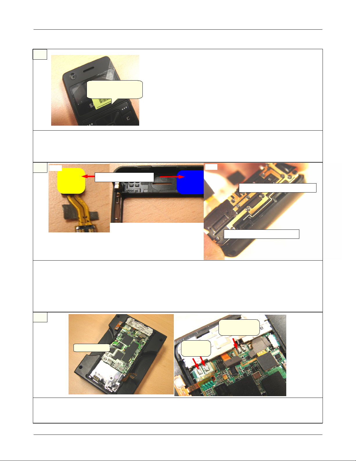
8 Point of important management
Press again!
Remove
the paper
Remove the paper of sub LCD
Remove the paper of sub LCD
1)
Put down the sub LCD connector at board.
2)
caution
※
Be care of scratch and molding damage.
1)
Condition between sub
LCD and B'd
2-10
SAMSUNG Proprietary-Contents may change without notice
This Document can not be used without Samsung's authorization
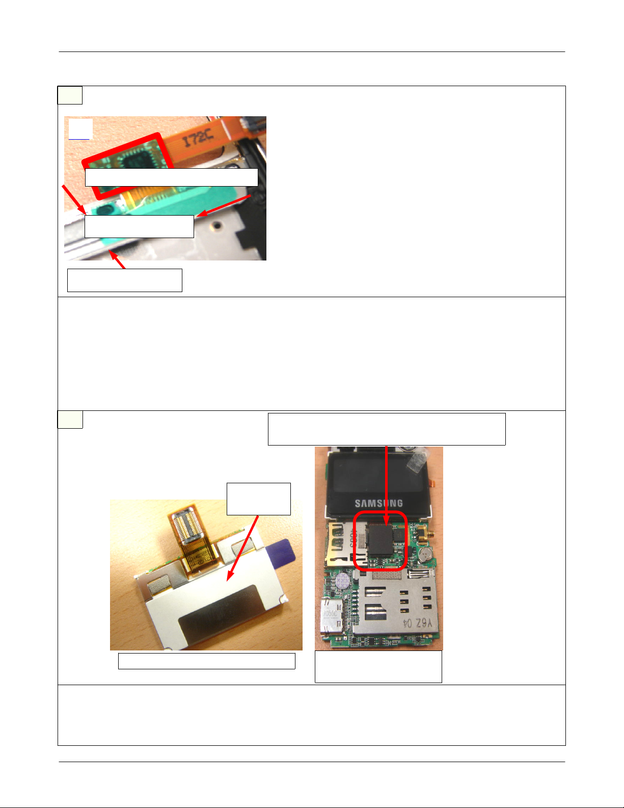
9
switching PN
label's position
Assemble board and cover.
1)
After assembling PBA, switching PN label's position on sub LCD.
2)
caution
※
Be care of scratch and molding damage.
1)
10
①
Get rid of papers
Main Electrical Parts List
②
Assembling hook's part
Assembling hook's part
Remove the paper of camera lens at phone cover.
1)
Get rid of paper at camera.
2)
Assemble between intenna and front part.
3)
After setting screw's hole of intenna and hole's rib of screw, put down the intenna.
4)
caution
※
Be care of scratch and molding damage.
1)
11
soldering
part
Put B'D on JIG
Excute soldering work for intenna at Board.
1)
caution
※
Be care of scratch and molding damage.
1)
soldering
part
2-11
SAMSUNG Proprietary-Contents may change without notice
This Document can not be used without Samsung's authorization
Main Electrical Parts List
12
SPK sponge
Insert shieldcan in the lower part
of intenna
After assembling shieldcan at board following fig.1, Insert SPK and camera connectors following fig.2.
1)
Attach poron sponge on SPK and camera connectors.
2)
caution
※
Be care of scratch and molding damage.
1)
CAMERA
sponge
13
sheet
ⓛ
sheet
②
sheet
③
Attach sheet No.1,2,3,4,5 at the decided positions following fig.
1)
Attach tape No.6 at the decided position following fig.
2)
caution
※
Be care of scratch and molding damage.
1)
tape
⑥
sheet
sheet
⑤
④
2-12
SAMSUNG Proprietary-Contents may change without notice
This Document can not be used without Samsung's authorization
14
Remove the
박리지 제
paper
거
Main Electrical Parts List
Insert LCD connector at
shieldcan'hole
<Remove the paper>
<Insert connector>
Put down
connector
> Put down the main LCD connector
Attach the side key at shieldcan.
1)
Get rid of3papers at the MAIN LCD back side.
2)
Insert the MAIN LCD connector at shieldcan's hole.
3)
put down the LCD connector.
4)
Atfer pushing camera and SPK connectors again, putting down the MAIN LCD connector.
5)
caution
※
Be care of scratch and molding damage.
1)
15
TAPE
B
Insert
battery
FPCB
Insert
battery
TAPE
TAPE
C
A
Attach EMI
tape
Attach tape
of preventing
to come off
Remove the paper of battery FPCB fixing tape.
1)
Romeve the paper of battery fixing both faces tape.
2)
Insert battery FPCB.
3)
Insert battery.
4)
Attach EMI tape A,B at the upper side of key connector.
5)
Attach an insulated tape at the upper side of battery FPCB connector.
6)
Put down main key connector following the fig.4.
7)
caution
※
Be care of scratch and molding damage.
1)
2-13
SAMSUNG Proprietary-Contents may change without notice
This Document can not be used without Samsung's authorization
Main Electrical Parts List
16
①
Insert the Touch key connector.
1)
Assemble the top portion.
2)
Assemble the right side.
3)
Assemble the left side.
4)
Assemble the lower end.
5)
Remove the both side of key fixing tape.
6)
Test hold key and mode key's action and tension.
7)
Excute volume key test.
8)
caution
※
Be care of scratch and molding damage.
1)
Be care of break
away the connector
> Main Key connector conclusion part
17
screw entering part
screw entering part
screw entering
part
Screw down following screw entering's flow chart.
1)
caution
※
Be care of scratch and molding damage.
1)
SAMSUNG Proprietary-Contents may change without notice
This Document can not be used without Samsung's authorization
2-14
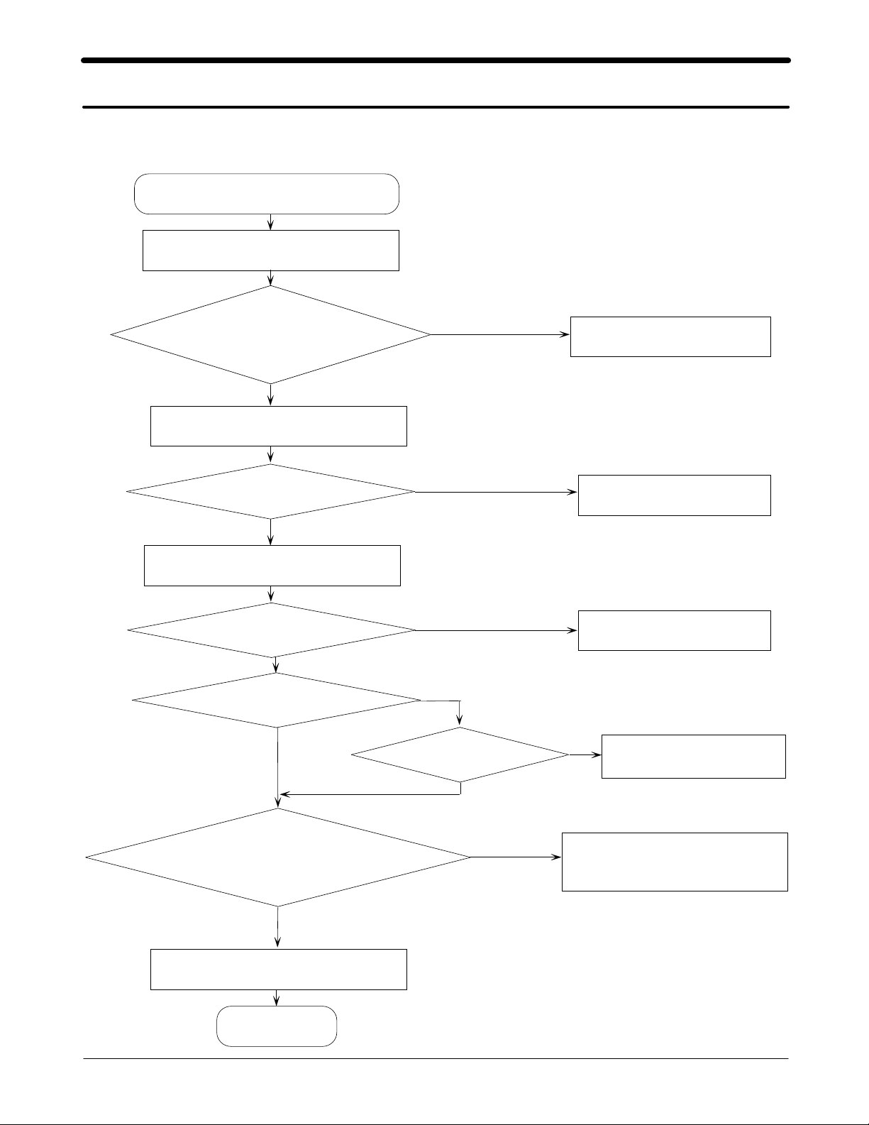
3. Flow Chart of Troubleshooting
Baseband
3-1.
3-1-1.
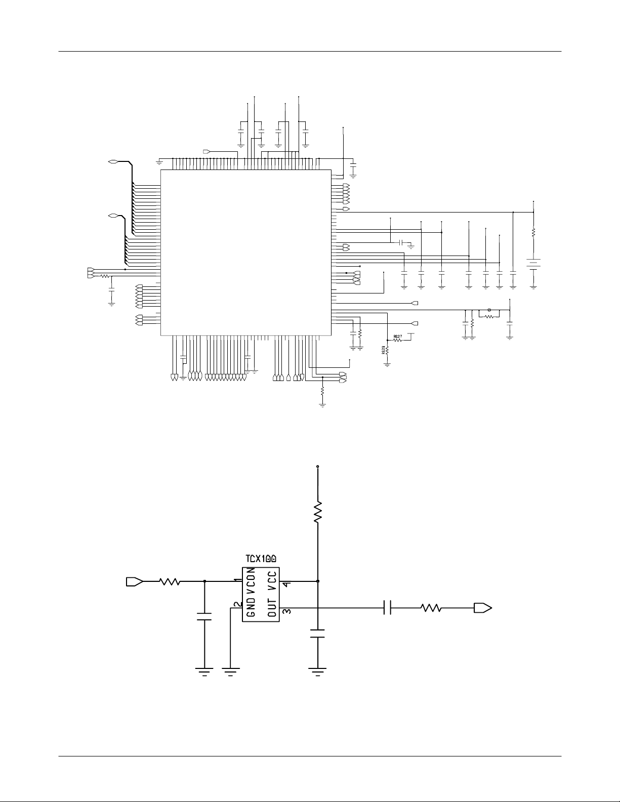
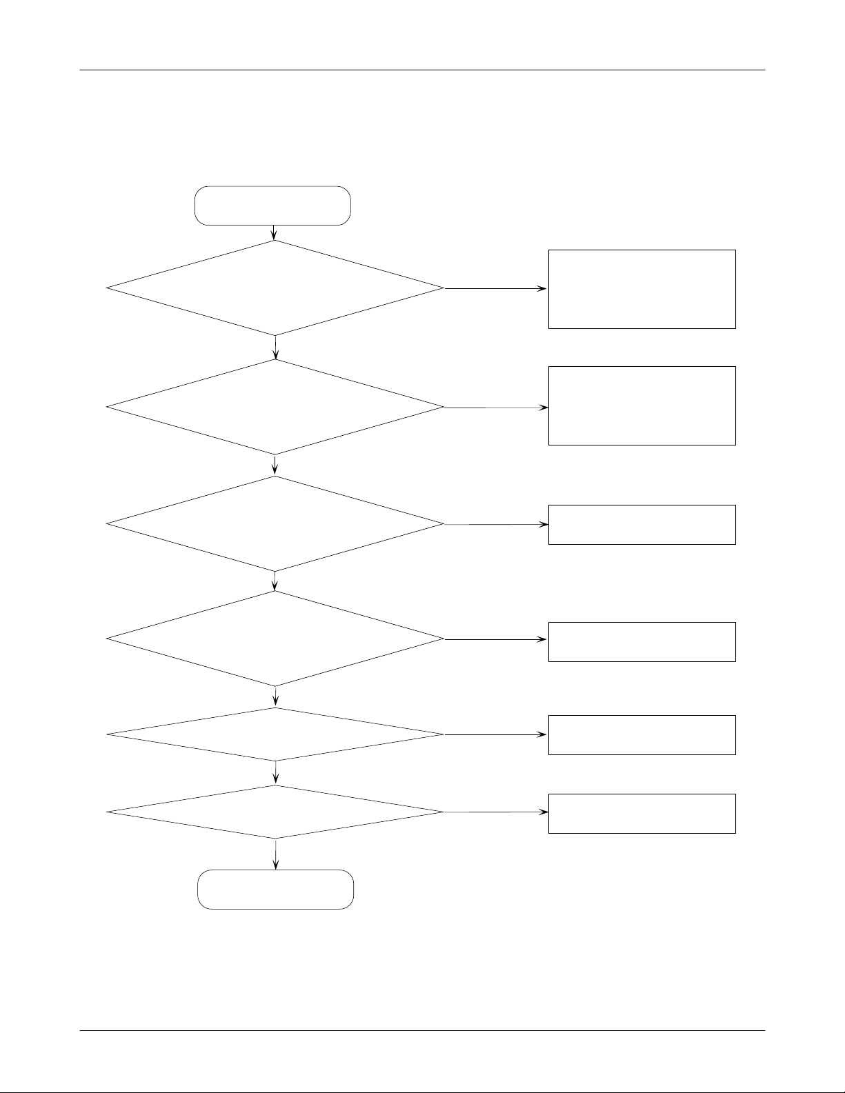
Power ON
Power ON' Does not work
'
Check the current consumption
Current consumption
100mA?
YES
Check the battery voltage
Voltage
Check the pins of
YES
3.3V ?
NO
Down load again
NO
Charge the Battery
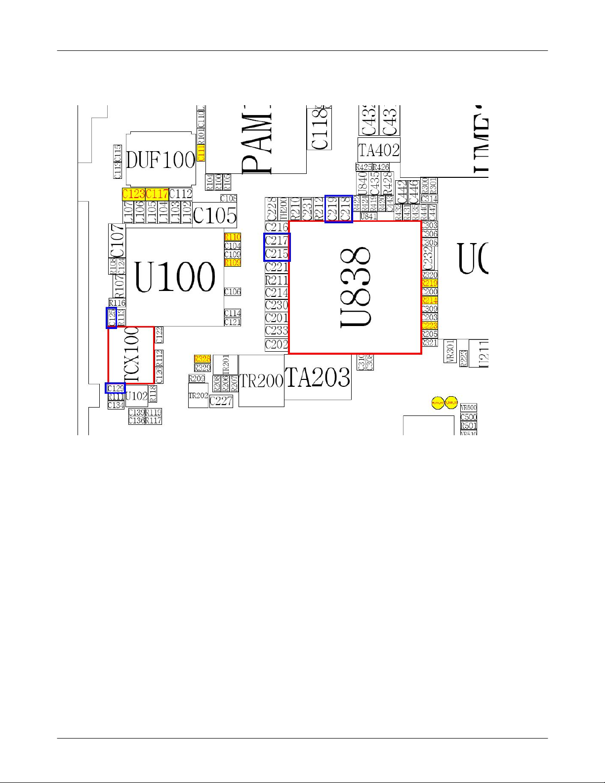
U838
C2151.8V ?
YES
and
C217
Check the clock signal
Freq.=26MHz,Vrms
Check the Initial operation
C218 = 2.8
YES
at pin#3of TCX10
YES
END
V?
300
0
mV
NO
C219=1.5
YES
3-1
V?
NO
NO
Check
NO
Check
Check the clock generation circuit
U838
U838
TCX10
and
0
C215
and
C219
SAMSUNG Proprietary-Contents may change without notice
This Document can not be used without Samsung's authorization
Flow Chart of Troubleshooting
DSP_IO
DSP_RWN
FLASH_RESET
DSP_DB(0:15)
DSP_AB(0:8)
T_DSP_IO
R205
3
2
2
C
BAND_SEL
MOD_SEL
TX_EN
XOENA
SX_EN
PAC_EN
RX_EN
SERLE
SERDAT
SERCLK
DSP_AB(8)
DSP_AB(7)
DSP_AB(6)
DSP_AB(5)
DSP_AB(4)
DSP_AB(3)
DSP_AB(2)
DSP_AB(1)
DSP_AB(0)
DSP_DB(15)
DSP_DB(14)
DSP_DB(13)
DSP_DB(12)
DSP_DB(11)
DSP_DB(10)
DSP_DB(9)
DSP_DB(8)
DSP_DB(7)
DSP_DB(6)
DSP_DB(5)
DSP_DB(4)
DSP_DB(3)
DSP_DB(2)
DSP_DB(1)
DSP_DB(0)
D2
D3
E3
E2
F3
F2
F1
F4
G4
G3
H5
J6
J5
K3
K2
K1
K5
K7
M1
M2
N2
N1
L5
P1
K6
L3
L2
R3
E6
C5
F5
E5
A4
G6
B3
A3
B1
A2
C1
C2
DB15
DB14
DB13
DB12
DB11
DB10
DB9
DB8
DB7
DB6
DB5
DB4
DB3
DB2
DB1
DB0
AB8
AB7
AB6
AB5
AB4
AB3
AB2
AB1
AB0
I|O
RWN
RESETN_CSP
OCTL0
OCTL1
OCTL2
OCTL3
OCTL4
OCTL5
OCTL6
OCTL7
SERLE1
SERLE2
SERDA
SERCK
VRF_2.8V
C202
VCCA_2.8V
VCCD_2.8V
HPEIO_1.8V
C200
C201
3
0
2
C
VBAT
EAR_ADC
7
F
1
S
D
N
G
P
N
I
X
U
A
3
1
D
3
C
D
A
_
X
U
A
N
N
I
X
U
A
4
1
L
P
N
I
X
U
A
4
B
L
T
C
O
_
D
N
G
U838
N
P
T
T
U
U
O
O
X
X
U
U
A
A
3
3
1
1
L
K
P
N
T
N
I
U
X
O
U
X
A
U
A
0
1
3
1
1
4
2
4
1
6
1
6
6
1
F
M
C
P
N
L
A
K
R
P
2
3
4
L
V
V
B
D
D
B
T
C
O
_
D
D
V
3
1
R
N
T
U
O
X
U
A
S
S
S
D
D
D
D
D
D
S
S
S
D
N
N
N
D
D
V
V
V
V
V
V
G
G
G
K
Q
L
N
P
A
M
C
K
I
N
O
N
G
_
G
C
C
D
R
D
I
I
I
I
E
E
E
C
V
A
T
A
A
A
R
R
X
O
D
V
R
D
V
D
D
V
X
4
4
4
3
6
6
4
1
1
1
L
P
R
N
D
M
R
M
2
3
2
C
K
2
3
K
L
C
5
0
3
5
1
3
5
6
1
1
5
1
1
8
1
4
3
J
N
F
G
J
M
N
B
E
C
B
K
3
1
2
1
S
O
I
S
_
V
D
D
V
4
X
U
A
_
C
C
D
M
A
6
5
R
P
P
Q
S
A
C
N
_
E
M
O
3
X
1
K
L
C
7
1
2
5
1
2
R
Q
6
D
D
D
D
C
C
O
I
D
_
V
D
D
V
R
T
N
I
D
3
P
T
N
I
_
P
S
D
VDD34
U
D
D
S
S
D
D
D
C
N
D
P
P
V
V
V
VDD12
H
G
_
_
V
_
D
D
D
N
N
N
G
G
UP_CLK
G
UP_RST
UP_IO
SIM_IO
SIM_RST
SIM_CLK
VSIM
VRTC
LED2_DRV
LED1_DRV
RING_DRV
VIB_DRV
VLDO_7
VLDO_6
VL5S_B
VL5S_A
VLDO_5
VL4S_B
VL4S_A
VLDO_4
VLDO_3
VLDO_2
VLDO_1
VACC
CSN_PSC
SCLK_PSC
SDO_PSC
SDI_PSC
VEXT
VBAT
CH_BDRV
CH_ISEN
CH_RES
ADC_AUX2
ADC_AUX1
VREF
CREF
N
N
E
P
F
1
2
_
RTC_ALMN
E
U
O
G
E
W
W
B
_
N
K
S
S
_
T
E
_
_
_
Q
1
R
E
_
D
R
R
R
R
S
W
T
B
O
E
I
S
W
W
W
N
M
V
R
P
P
P
P
I
0
9
7
9
9
5
4
0
1
1
1
1
L
L
K
M
L
N
C
C
F
N
N
R214
U
O
O
B
_
_
_
R
G
I
1
J
W
W
P
S
P
0
1
1
2
K
5
6
7
1
C
C
S
N
N
D
N
G
C
P
F
X
T
A
7
9
E
D
C
C
F
P
A
A
V
0
0
9
1
8
J
J
J
6
5
4
1
1
1
S
S
S
D
D
D
N
N
N
G
G
G
1
2
P
F
F
I
E
E
X
R
R
T
X
A
A
R
R
R
6
7
6
5
D
D
B
B
3
3
2
C
P
I
_
X
T
R
0
1
8
9
7
6
7
8
9
1
8
7
H
J
2
3
1
1
S
S
D
D
N
N
G
G
P
N
I
Q
X
X
T
T
X
X
R
R
7
C
N
I
_
X
T
R
9
G
G
G
F
G
F
H
F
H
H
8
9
2
6
7
4
5
0
3
1
1
1
S
S
S
S
S
S
S
S
S
S
D
D
D
D
D
D
D
D
D
D
N
N
N
N
N
N
N
N
N
N
G
G
G
G
G
G
G
G
G
G
N
P
N
P
P
N
N
Q
X
T
X
R
6
C
P
Q
_
X
T
R
T
T
A
N
A
B
P
B
U
U
T
T
T
T
N
N
I
I
O
O
U
U
U
U
C
C
C
C
I
I
I
I
O
O
O
O
A
M
A
A
A
M
M
M
5
4
2
2
2
1
4
5
5
1
1
1
1
1
1
1
1
1
P
P
P
N
R
N
N
M
M
N
P
P
P
P
N
N
N
N
T
Q
_
X
T
R
T
N
A
B
N
A
B
I
I
U
T
T
U
T
T
C
C
I
I
U
U
O
U
U
O
C
M
O
O
M
C
O
O
I
I
A
A
A
A
M
M
C11
J13
N9
R10
P10
J11
K11
K14
K12
H11
G12
G13
F13
F15
C12
A14
C9
D10
B10
B11
A12
B12
A13
J12
G11
F14
TP_CSN_PSC
K8
L8
N7
M7
E14
E13
E11
F12
D14
D15
E10
A10
E9
H10
C230
VBAT
INTRQ
PWR_KEEP
RST
C209
SIMCLK
SIMRST
SIMDATA
SIM_IO
SIM_RST
SIM_CLK
VSIM
DCS_TX_EN
GSM_TX_EN
TP_VACC
UP_CS
UP_SCLK
UP_SDO
UP_SDI
R211
VCCB_2.9V
VBAT
VRTC_1.5V
VLDO_1.8V
VCCA_2.8V
VRF_2.8V
VCCD_2.8V
VLDO_1.5V
R204
C214
1
C221
SUB_BATT
C215
ICHRG
RTCALARM
C216
C218
C217
C219
VCCB_2.9V
TH200
R210
1
2
3
1
2
2
C
R
C228
BAT200
C220
2
AFC
R112
C126
VRF_2.8V
R111
3-2
C129
C125
R113
CLK26M
SAMSUNG Proprietary-Contents may change without notice
This Document can not be used without Samsung's authorization
Flow Chart of Troubleshooting
3-3
SAMSUNG Proprietary-Contents may change without notice
This Document can not be used without Samsung's authorization
Flow Chart of Troubleshooting
3-1-2.
Initial
Initial Failure
The voltage at the
The voltage at the
The voltage at the VR301
Low
"
There is
form at the
C215=1.8
C218=2.8
YES
High"
-->
YES
KHz wave
32.768
C317, C318 ?
V?
V?
?
NO
NO
NO
Check the
If it has some problem,
(
it has to be replaced.)
Check the
If it has some problem,
(
it has to be replaced.)
Check the UCP
U838
U838
300
YES
The voltage is
at the
C216,C217,C218 ?
LCD Display OK
Sound operation OK
END
2.8V
YES
YES
YES
NO
?
?
NO
NO
Check the
Check the LCD part
Check the Audio part
U838
3-4
SAMSUNG Proprietary-Contents may change without notice
This Document can not be used without Samsung's authorization
Flow Chart of Troubleshooting
D(0:15)
CP_WEN
CP_OEN
FLASH_RESET
ROM1_CS
ROM2_CS
RAM1_CS
MV_CS
LOWER_BYTE
UPPER_BYTE
A(0:25)
D(0)
D(1)
D(2)
D(3)
D(4)
D(5)
D(6)
D(7)
D(8)
D(9)
D(10)
D(11)
D(12)
D(13)
D(14)
D(15)
TP_WEN
TP_ROM1_CS
TP_RAM1_CS
TP_MV_CS
A(0)
A(1)
A(2)
A(3)
A(4)
A(5)
A(6)
A(7)
A(8)
A(9)
A(10)
A(11)
A(12)
A(13)
A(14)
A(15)
A(16)
A(17)
A(18)
A(19)
A(20)
A(21)
A(22)
A(23)
A(24)
SIMCLK
SIMDATA
SIMRST
USB_SUSP
USB_DET
D_SCL_HPE
USB_VPO
USB_VMO
USB_OEN
USB_DATA
UP_SCLK
UP_SDO
UP_SDI
UP_CS
USB_ON
AMP_EN
D_SDA_HPE
BT_CTS
BT_TXD
BT_RXD
BT_RTS
BT_EN
RADIO_SEL
VIB_EN
SDS_TXD
SDS_RXD
KEY_COL(0:4)
PSW1_BUF
KEY_ROW(0:4)
B7
A_A0
C8
A_A1
D8
A_A2
A6
A_A3
C6
A_A4
C5
A_A5
D7
A_A6
E7
A_A7
C4
A_A8
C2
A_A9
A3
A_A10
B3
A_A11
B1
A_A12
D6
A_A13
D5
A_A14
D3
A_A15
E8
A_A16
F8
A_A17
E6
A_A18
D2
A_A19
E4
A_A20
E3
A_A21
F5
A_A22
F4
A_A23
F3
A_A24
F2
PIO35_A_A25_BOOTSEL
A8
A_D0
E9
A_D1
F9
A_D2
G10
A_D3
G11
A_D4
F11
A_D5
E11
A_D6
G12
A_D7
D11
A_D8
E12
A_D9
C12
A_D10
A12
A_D11
F12
A_D12
D12
A_D13
E13
A_D14
D13
A_D15
D14
A_WEN
B14
A_OEN
E14
PIO30_WAITN
H14
FLASHRSTN
A14
A_CS0N
C15
A_CS1N
G14
A_CS2N
J14
A_CS3N
D15
A_CS4N
C16
A_CS5N
F15
A_CS6N
B17
A_CS7N
H16
A_BE0N
A17
A_BE1N
2
1
2
1
C
C
N
N
K
L
O
C
I
M
M
I
I
S
S
2
4
T
P
KEY_COL(0)
KEY_COL(1)
KEY_COL(2)
KEY_COL(3)
KEY_COL(4)
T
S
R
M
I
S
_
4
1
O
I
P
5
P
KEY_ROW(0)
KEY_ROW(1)
KEY_ROW(2)
KEY_ROW(3)
KEY_ROW(4)
HP_CORE_1.57V
C311
2
1
8
1
7
1
1
1
1
1
F
R
M
T
F
8
U
D
D
U
1
_
_
_
_
S
A
A
A
A
S
S
S
D
D
V
S
S
D
D
V
V
V
V
P
O
I
N
S
O
I
E
P
M
U
M
P
O
V
V
S
V
V
_
_
_
_
_
_
B
B
B
B
B
B
S
S
S
S
S
S
U
U
U
U
U
U
_
_
_
_
_
_
6
2
1
3
7
9
3
1
1
1
0
0
O
O
O
O
O
O
I
I
I
I
I
I
P
P
P
P
P
P
7
8
6
9
6
9
1
1
1
1
1
1
F
B
E
D
C
C
C310
8
1
G
1
C
_
T
8
R
P
V
1
_
O
I
_
D
D
V
Q
E
R
K
L
C
S
Y
S
_
0
2
O
I
P
5
9
1
G
P
2
4
5
2
1
1
1
1
R
G
W
W
I
S
N
N
K
T
T
M
C
S
S
T
E
R
T
R
IOBIT1_PIO06
IOBIT0_PIO05
SPTXD1_I2SD_PIO16
SPRXD1_PIO17
SPCLK1_PIO18
CPTSTSTOP_CKO
6
4
O
I
P
_
1
0
7
6
5
1
2
2
2
M
O
O
O
O
I
I
I
I
W
P
P
P
P
P
7
9
6
9
1
1
1
1
V
V
U
U
C318
VRTC_1.5V
CKO_IACK
SPFS1_PIO15
D_D15
D_D14
D_D13
D_D12
D_D11
D_D10
TEST3
TEST2
TEST1
ATDO_PWM2
ATDI_RTS1
ATCK_CTS1
ATMS_PIO45
PIO31_IRQ6
PIO00_IRQ5
PIO47
PIO34
PIO33
8
2
2
3
O
O
I
I
P
P
7
3
1
1
R
W
C304
CLK13M_HPE
TR_RST
T12
TDO
V14
TDI
U14
TCK
N12
N11
V12
N15
N16
M17
M18
T15
INT0
W6
IO
V6
RWN
P11
N10
N9
N8
P9
P8
R9
D_D9
T9
D_D8
T8
D_D7
U8
D_D6
V8
D_D5
R8
D_D4
T7
D_D3
R7
D_D2
T6
D_D1
U6
D_D0
R6
D_A8
N6
D_A7
V4
D_A6
T5
D_A5
U4
D_A4
V3
D_A3
W3
D_A2
W2
D_A1
V1
D_A0
V16
T14
GND
U15
T17
TDOTP_OEN
T13
TDI
L5
TCK
M4
K12
TMS
P12
P16
IRQ4
P18
IRQ3
P17
IRQ2
M19
IRQ1
M16
J16
R14
U18
DSP_DB(15)
DSP_DB(14)
DSP_DB(13)
DSP_DB(12)
DSP_DB(11)
DSP_DB(10)
DSP_DB(9)
DSP_DB(8)
DSP_DB(7)
DSP_DB(6)
DSP_DB(5)
DSP_DB(4)
DSP_DB(3)
DSP_DB(2)
DSP_DB(1)
DSP_DB(0)
HOLD
KEY_EL_ON
PCM_SYNC
PCM_IN
PCM_OUT
PCM_CLK
DSP_INT
DSP_IO
DSP_RWN
DSP_AB(8)
DSP_AB(7)
DSP_AB(6)
DSP_AB(5)
DSP_AB(4)
DSP_AB(3)
DSP_AB(2)
DSP_AB(1)
DSP_AB(0)
CP_TDO
CP_TDI
CP_TCK
CP_TMS
R_RW
CARD_INS
MV_INT
JACK_IN
INTRQ
MODE_SELECT
USB_CON
LCD_CON
CHG_OFF
EAR_SWITCH
MVCORE_ON
MP3_ENABLE
MIC_AMP_EN
DAC_RESET
SUB_BATT_SW
XOENAQ
PWR_KEEP
CLK32K
RTCALARM
DSP_DB(0:15)
DSP_AB(0:8)
R304
HP_CORE_1.57V
C303
C302
C305
C306
0
1
2
1
0
2
9
1
1
8
1
1
1
8
8
7
1
J
H
H
H
M
M
L
M
M
K
L
1
0
9
7
1
S
S
V
8
6
5
4
3
7
2
1
1
1
1
1
1
1
S
S
S
S
S
S
S
S
S
S
S
S
S
S
S
S
S
S
S
S
V
V
V
V
V
V
V
V
V
V
8
8
8
3
3
2
2
8
9
1
9
8
H
H
6
5
S
S
S
S
V
V
1
2
1
A
G
G
4
3
2
S
S
S
S
S
S
V
V
V
8
1
7
1
A
N
M
H
G
B
B
V
V
1
6
5
4
3
2
7
8
S
E
E
E
E
E
E
E
S
R
R
R
R
R
R
R
V
O
O
O
O
O
O
O
C
C
C
C
C
C
C
_
_
_
_
_
_
_
D
D
D
D
D
D
D
D
D
D
D
D
D
D
V
V
V
V
V
V
V
HPEIO_1.8V
C307
8
2
1
8
1
5
1
W
W
U
U
U
8
4
5
6
7
1
1
1
1
1
1
E
_
_
_
_
_
R
8
8
8
8
8
O
P
P
P
P
P
1
C
1
1
1
1
_
_
_
_
_
_
D
O
O
O
O
O
I
I
I
I
I
D
_
_
_
_
_
V
D
D
D
D
D
D
D
D
D
D
V
V
V
V
V
C309
C308
8
4
2
8
1
T
3
1
_
8
P
1
_
O
I
_
D
D
V
6
6
1
9
1
1
6
1
4
1
L
L
P
0
1
2
1
1
1
_
_
_
8
8
8
P
P
P
1
1
1
_
_
_
O
O
O
I
I
I
_
_
_
D
D
D
D
D
D
V
V
V
4
1
1
1
B
F
D
D
B
C
C
B
B
2
3
9
8
7
6
5
4
_
_
_
_
_
_
_
_
8
8
8
8
8
8
8
8
P
P
P
P
P
P
P
P
1
1
1
1
1
1
1
1
_
_
_
_
_
_
_
_
O
O
O
O
O
O
O
O
I
I
I
I
I
I
I
I
_
_
_
_
_
_
_
_
D
D
D
D
D
D
D
D
D
D
D
D
D
D
D
D
V
V
V
V
V
V
V
V
UCP300
F
U
B
A
T
A
D
D
_
S
B
2
I
S
_
0
U
0
0
_
D
D
0
K
7
X
L
X
S
3
T
R
F
C
O
P
P
P
I
P
S
S
S
P
S
4
2
7
3
3
1
T
R
U
R
E
X
T
4
2
3
9
4
A
4
0
0
8
2
0
1
D
2
O
O
O
O
0
O
I
I
I
I
I
R
Q
I
O
P
P
P
P
P
I
_
R
_
_
_
_
_
I
P
1
0
0
0
0
0
_
_
4
D
0
R
S
R
S
0
O
O
X
C
S
T
T
I
T
I
X
P
R
D
D
C
D
R
T
R
6
1
2
4
6
5
3
3
2
1
P
P
N
N
N
M
M
M
R
_
1
W
X
S
R
P
A
8
_
1
D
2
1
0
R
Q
I
D
D
_
R
R
R
I
2
B
B
_
4
1
Y
Y
1
O
X
E
I
E
X
K
P
K
R
T
6
7
6
7
7
J
J
1
L
K
R
0
7
6
5
4
3
2
D
R
B
Y
E
K
5
J
1
1
9
8
D
D
D
D
D
D
D
D
D
R
R
R
R
R
R
R
R
R
B
B
B
B
B
B
B
B
B
Y
Y
Y
Y
Y
Y
Y
Y
Y
E
E
E
E
E
E
E
E
E
K
K
K
K
K
K
K
K
K
1
4
6
8
2
4
4
6
3
J
J
H
H
H
H
H
G
G
N
N
N
E
E
E
_
_
_
0
3
2
0
1
D
T
T
T
K
M
A
A
A
L
C
C
D
D
D
_
_
_
_
_
I
I
I
I
I
C
C
C
C
C
M
M
M
M
M
_
_
_
_
_
8
8
3
2
1
3
0
2
2
2
O
O
O
O
O
I
I
I
I
I
P
P
P
P
P
5
3
3
2
3
1
1
1
1
1
J
J
L
L
K
P
D
T
T
T
E
A
M
A
A
E
D
C
D
D
K
N
_
_
_
_
R
I
I
I
I
T
M
C
C
C
C
U
W
R
M
M
P
M
M
O
A
_
_
_
_
_
2
L
C
C
0
9
9
3
4
3
A
T
T
4
3
1
4
2
C
C
R
R
O
O
O
O
O
S
T
1
I
I
I
2
I
I
X
P
O
P
P
X
P
R
P
9
9
6
4
4
4
5
7
5
1
1
1
1
1
1
1
1
1
L
L
F
P
H
N
H
G
M
C317
OSC300
CHG_DET
MP3_SDA
MP3_SCL
CF
HPEIO_1.8V
R324
R323
D_SCL
D_SDA
MV_RST
VBUS_GPIO
R326
R327
R325
FLIPPER_USB
3-5
SAMSUNG Proprietary-Contents may change without notice
This Document can not be used without Samsung's authorization
 Loading...