Samsung E1310B Service Manual

GSM TELEPHONE
GT-E1310B
GSM TELEPHONE
CONTENTS
Safety Precautions
1.
Specification
2.
Product Function
3.
Array course control
4.
Exploded View and Parts list
5.
MAIN Electrical Parts List
6.
Block Diagrams
7.
PCB Diagrams
8.
Chart of Troubleshooting
9.
Reference data
10.
Disassembly and Assembly
11.
Instructions

Safety Precautions
1.
Repair Precaution
1-1.
Repair in Shield Box, during detailed tuning. Take specially care of tuning or test, because
―
specipicty of cellular phone is sensitive for surrounding interference(RF noise).
Be careful to useakind of magnetic object or tool, because performance of parts is damaged by
―
the influence of magnetic force.
Surely useastandard screwdriver when you disassemble this product, otherwise screw will be
―
worn away.
Useathicken twisted wire when you measure level.
―
thicken twisted wire has low resistance, therefore error of measurement is few.
A
Repair after separate Test Pack and Set because for short danger(for example an overcurrent
―
and furious flames of parts etc) when you repair board in condition of connecting Test Pack and
tuning on.
Take specially care of soldering, because Land of PCB is small and weak in heat.
―
Surely tune on/off while using AC power plug, becausearepair of battery charger is dangerous
―
when tuning ON/OFF PBA and Connector after disassembling charger.
Don't use as you pleases after change other material than replacement registered on SEC System.
―
Otherwise engineer in charge isn't charged with problem that you don't keep this rules.
1-1
SAMSUNG Proprietary-Contents may change without notice
This Document can not be used without Samsung's authorization

Safety Precautions
ESD(Electrostatically Sensitive Devices) Precaution
1-2.
Several semiconductor may be damaged easily by static electricity. Such parts are called by ESD
Electrostatically Sensitive Devices), for example IC,BGA chip etc. Read Precaution below.
(
You can prevent from ESD damage by static electricity.
Remove static electricity remained your body before you touch semiconductor or parts with
―
semiconductor. There are ways that you touch an earthed place or wear static electricity prevention
string on wrist.
Use earthed soldering steel when you connect or disconnect ESD.
―
Use soldering removing tool to break static electricity.,otherwise ESD will be damaged by static
―
electricity.
Don't unpack until you set up ESD on product. Because most of ESD are packed by box and
―
aluminum plate to have conductive power,they are prevented from static electricity.
You must maintain electric contact between ESD and place due to be set up until ESD is
―
connected completely to the proper place oracircuit board.
1-2
SAMSUNG Proprietary-Contents may change without notice
This Document can not be used without Samsung's authorization

Specification
2.
2-1.
GSM General Specification
Freq. Band[MHz]
Uplink/Downlink
ARFCN range 0~124 & 975~1023 512~885
Tx/Rx spacing 45MHz 95MHz
Mod. Bit rate/
Bit Period
Time Slot Period/Frame
Period
EGSM 900 DCS1800
880~915
925~960
270.833kbps
3.692us
576.9us
4.615ms
1710~1785
1805~1880
270.833kbps
3.692us
576.9us
4.615ms
Modulation 0.3GMSK 0.3GMSK
MS Power 33dBm~5dBm 30dBm~0dBm
Power Class
Sensitivity -102dBm -100dBm
TDMA Mux 8 8
Cell Radius 35Km 2Km
max
(
4
+33
dBm)
max
(
1
+30
dBm)
2-1
SAMSUNG Proprietary-Contents may change without notice
This Document can not be used without Samsung's authorization

Specification
2-2.
GSM TX power class
TX Power
control level
533±2
631±2
729±2
827±2
925±2
10 23±2
11 21±2
GSM900
dBm
dBm
dBm
dBm
dBm
dBm
dBm
TX Power
control level
0 30±3
1 28±3
2 26±3
3 24±3
4 22±3
5 20±3
6 18±3
DCS1800
dBm
dBm
dBm
dBm
dBm
dBm
dBm
12 19±2
13 17±2
14 15±2
15 13±2
16 11±3
17 9±3
18 7±3
19 5±3
dBm
dBm
dBm
dBm
dBm
dBm
dBm
dBm
7 16±3
8 14±3
9 12±4
10 10±4
11 8±4
12 6±4
13 4±4
14 2±5
15 0±5
dBm
dBm
dBm
dBm
dBm
dBm
dBm
dBm
dBm
2-2
SAMSUNG Proprietary-Contents may change without notice
This Document can not be used without Samsung's authorization

Operation Instruction and Installation
3.
Main Function
GSM/GPRS Function Support
•
ARM926EJ-S Core
•
S20 Pin TA
•
No Java
•
Dual Band
•
Poly Ringtone(Midi,AMR,MP3)
•40
Non Camera
•
Phonebook
•
BT Support
•
(900/1800
500
MHz)
entry
3-1
SAMSUNG Proprietary-Contents may change without notice
This Document can not be used without Samsung's authorization

Array course control
4.
Software Adjustments
4-1.
Test Jig(GH
Test Cable(GH39-01160A) RF Test Cable(GH39-00
99-36900
A)
RF Test Cable(GH99-38251A)
985
A)
4-1
SAMSUNG Proprietary-Contents may change without notice
This Document can not be used without Samsung's authorization

Array course control
Software Downloading
4-2.
4-2-1.
•2
4-2-2.
•
•
•
•
•
•
Downloading Binary Files
binary files for downloading E1310B
E1310BXAIB2.cla
-
E1310BXAIB2.tfs
-
Pre-requsite for Downloading
Downloader Program
Gaia Downloader for SEC v04)
(
GT-E1310BMobile Phone
JIG BOX
Test Cable
Serial Cable
Binary files
4-2
SAMSUNG Proprietary-Contents may change without notice
This Document can not be used without Samsung's authorization
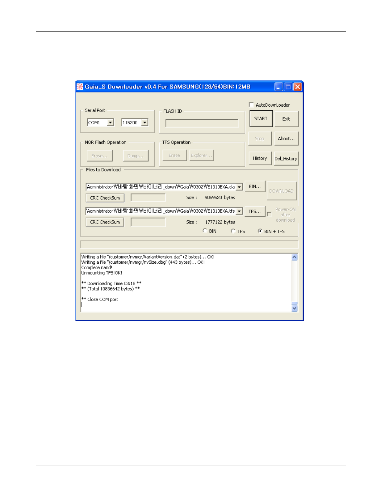
Array course control
4-2-3.
1.
S/W Downloader Program
Load the binary download program by executing the“Gaia Downloader for SEC v04
”.
4-3
SAMSUNG Proprietary-Contents may change without notice
This Document can not be used without Samsung's authorization
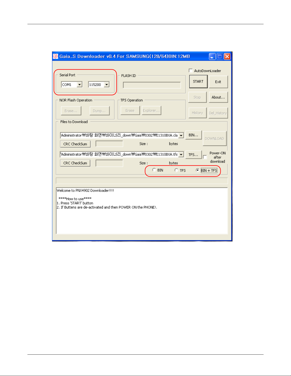
Array course control
Select the Port, Baud Rate and Mode
2.
.
4-4
SAMSUNG Proprietary-Contents may change without notice
This Document can not be used without Samsung's authorization
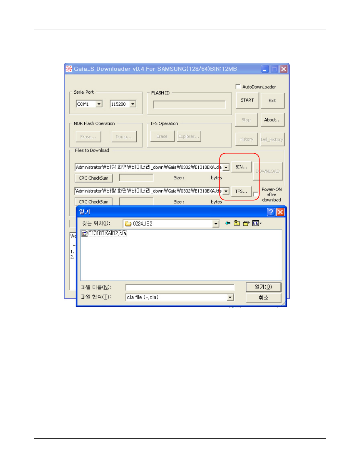
Select the binary fileswhat you want to download
3.
Array course control
4-5
SAMSUNG Proprietary-Contents may change without notice
This Document can not be used without Samsung's authorization
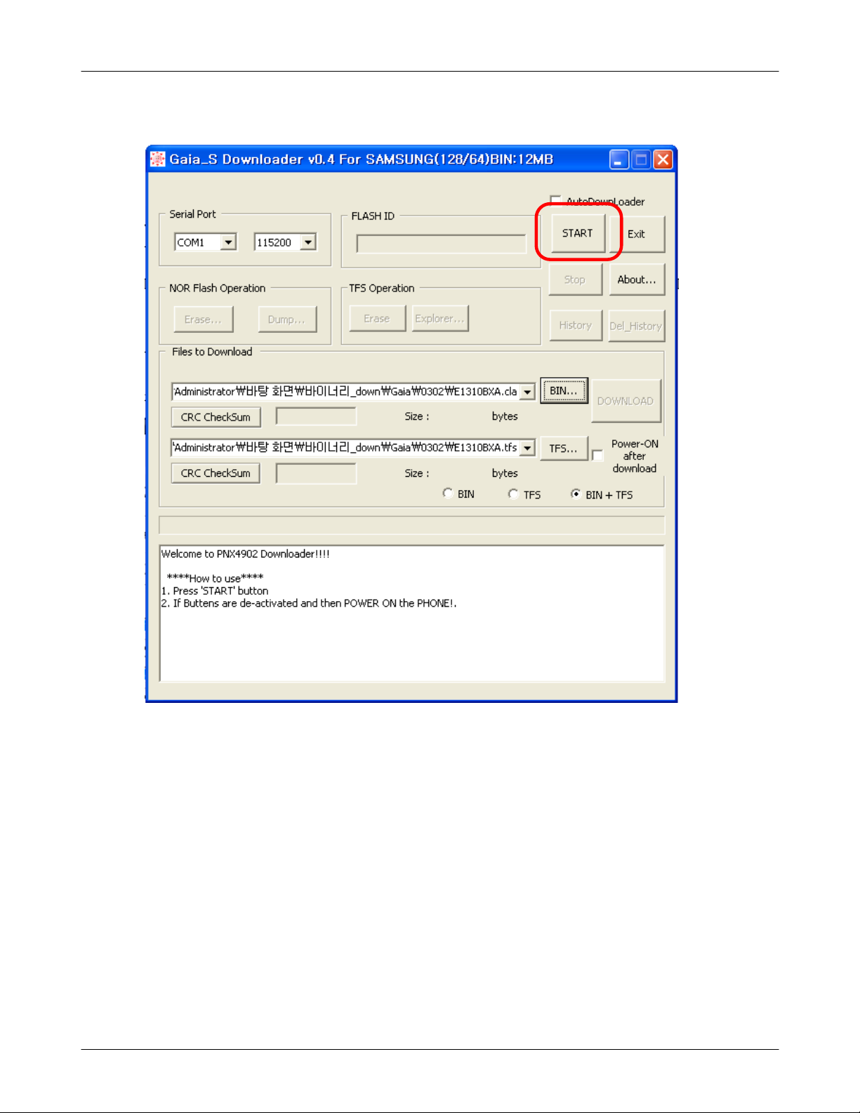
Array course control
ress the"Start" button and connect the Handset
4. P
4-6
SAMSUNG Proprietary-Contents may change without notice
This Document can not be used without Samsung's authorization
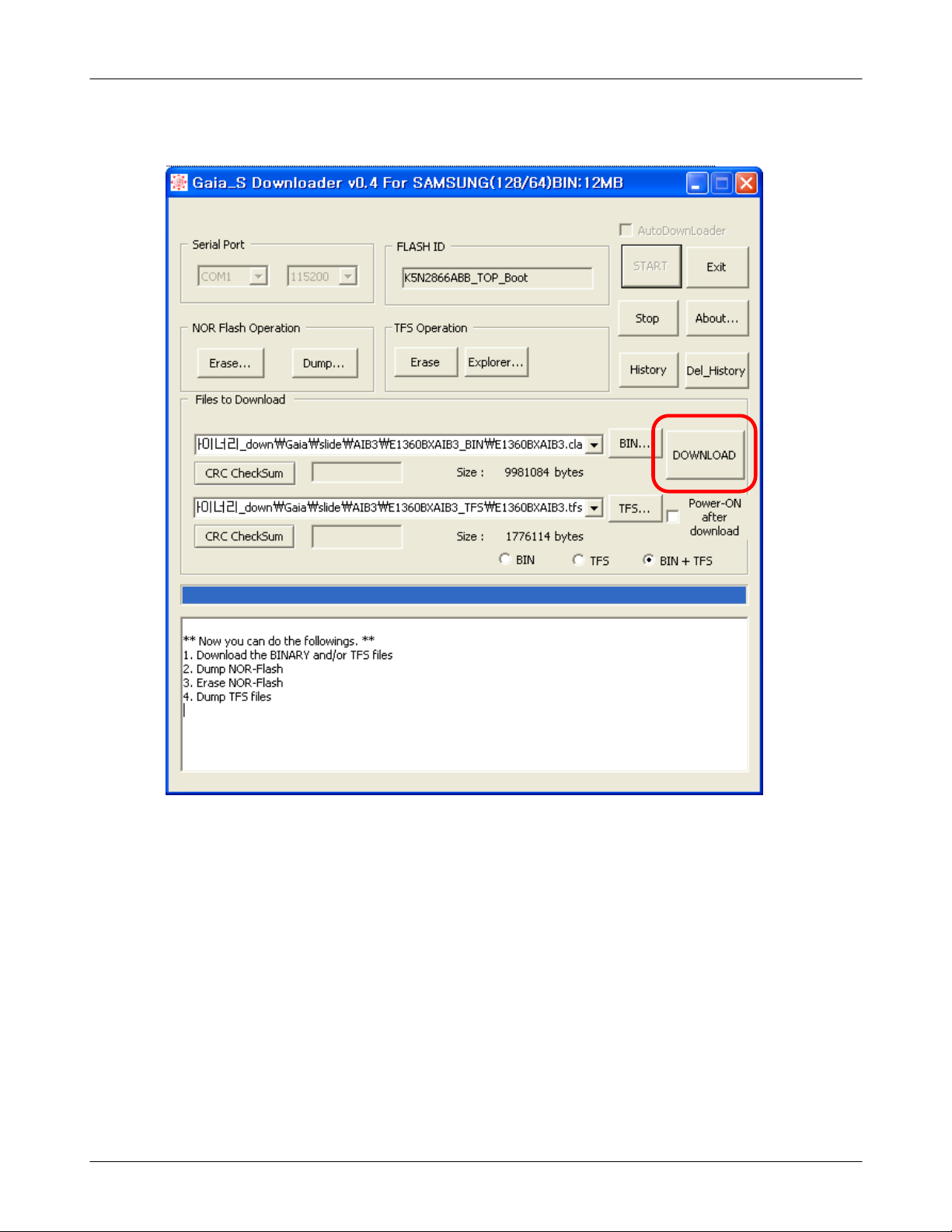
ress the"Download" butto
5P
Array course control
n.
4-7
SAMSUNG Proprietary-Contents may change without notice
This Document can not be used without Samsung's authorization
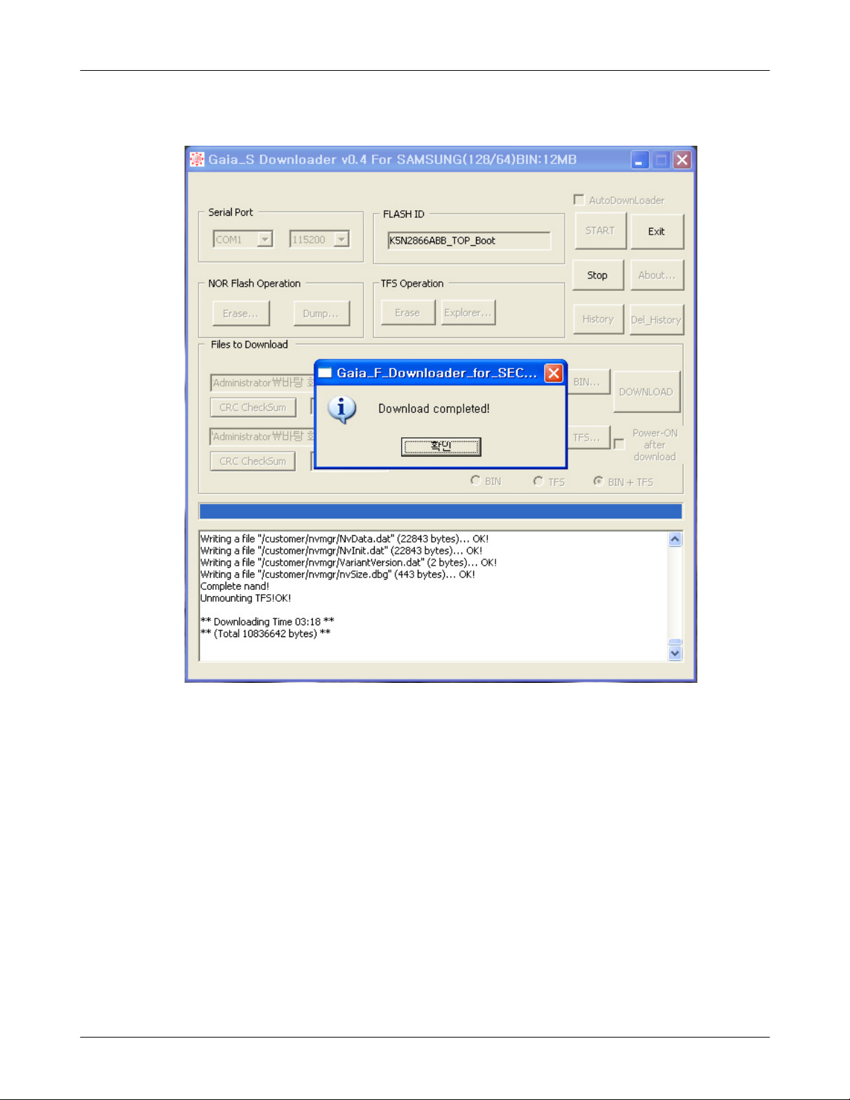
Array course control
When downloading is complete, automatically the small window was showed up.
6.
4-8
SAMSUNG Proprietary-Contents may change without notice
This Document can not be used without Samsung's authorization
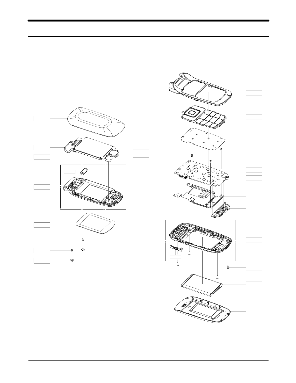
Exploded View and Parts List
5.
5-1.
QFU01
QPC01
QLC01
Cellular phone Exploded View
QSP01
QMO01
QHI01
QFR01
QKP01
QME01
QCR72
QMP01
QMI01
QFL01
QMW01
QCR72
QSC01
QSH01
QAN02
QRE01
QIF01
QCR60
QBA01
QBA00
5-1
SAMSUNG Proprietary-Contents may change without notice
This Document can not be used without Samsung's authorization

Exploded View and Parts List
5-2.
Cellular phone Parts list
Design LOC Description SEC CODE
QAN02 INTENNA-GTE1310S GH42-01867A
QBA00 PMO COVER-BATT GH72-51346A
QBA01 INNER BATTERY PACK-800MAH,BLK,UNI,MAIN GH43-03241A
QCR60 SCREW-MACHINE
QCR72 SCREW-MACHINE
6001-002005
6001-002051
QFR01 ASSY CASE-FRONT(VODA) GH98-12415A
QFU01 ASSY CASE-FOLDER UPPER GH98-11165A
QKP01 ASSY KEYPAD-(BLACK/OPEN) GH98-11207A
QMW01 PMO WINDOW-MAIN GH72-53167A
QLC01 ELA ETC-GTE1310S LCD HOT BAR SVC GH96-03745A
QME01 DOME SHEET-GT-E1310S GH59-06739A
QMI01 MICROPHONE-ASSY-SGH-T109 GH30-00513A
QMO01 MOTOR DC-SGHS342I GH31-00119A
QMP01 ASSY PBA MAIN-GT_E1310B GH92-05525A
QPC01 UNIT-GTE1310 CON TO CON FPCB GH59-06731A
QSC01 PMO COVER-SCREW CAP
L
GH72-51347A
QSH01 IPR COVER-SHIELD GH70-04574A
QSP01 SPEAKER
3001-002482
QFL01 ASSY CASE-FOLDER LOWER GH98-11166A
QHI01 ASSY HINGE GH98-03190A
QRE01 ASSY CASE-REAR GH98-11168A
QIF01 PMO COVER-IF GH72-51345A
5-2
SAMSUNG Proprietary-Contents may change without notice
This Document can not be used without Samsung's authorization

MAIN Electrical Parts List
6.
SEC CODE Design LOC Description
0401-001141
0403-001547
0406-001267
0406-001288
0406-001306
0601-002591
0601-002591
1001-001546
1009-001037
1108-000217
1201-002731
1203-005498
1203-005512
1205-003322
1205-003662
1404-001221
1405-001082
2007-000138
2007-000139
2007-000141
2007-000143
2007-000148
2007-000157
2007-000162
2007-000171
2007-000172
2007-000172
2007-000173
2007-001288
2007-001301
2007-001333
2007-007698
2007-008500
2203-000233
2203-000330
2203-000386
D201,D202
ZD200 TDZ5.6
ZD300 RCLAMP0521P
D300,D301 PESD5V0S1UL
ZD301,ZD302 CM1219-05SE
LED400,LED401,LED402 WH104-LC
LED403,LED404,LED405 WH104-LC
U30
1
U303 BU52031NVX
U202 K5N6433ABM-AD11
PAM100 SKY77534-11
U203 SUS6160MNTBG
U401 MIC5365-3.3YMT
U10
3
U201 PNX4902ET
TH200 NCP15WB473J04RC
VR301 VC040205X150R
R111,R308,R309,R315 RC1005J101CS
R303 RC1005J221CS
R300,R301,R304,R306 RC1005J222CS
R203,R204 RC1005J472CS
R201,R209 RC1005J103CS
R402 RC1005J473CS
R213 RC1005J104CS
R101 WR0402X000JT
R211,R305,R310,R320 RC1005J100CS
R321,R403 RC1005J100CS
R311,R316 RC1005J220CS
R108 MCR01MZP5J180
R210 MCR01MZP5J680
R214 MCR01MZP5J183
R207 RK73H1ETP5101F
R205 SR73H2BTDR100F
C228 GRP1555C1H101J
C320,C321 GRP1555C1H120J
C301,C304,C309 GRP1555C1H150J
SS400G
1
STG5223QTR
E-STLC2500DTR
6-1
SAMSUNG Proprietary-Contents may change without notice
This Document can not be used without Samsung's authorization

Main Electrical Parts List
SEC CODE Design LOC Description
2203-000425
2203-000438
2203-000679
2203-000696
2203-000812
2203-000812
2203-000812
2203-000812
2203-000995
2203-001072
2203-001153
2203-002443 C131
2203-002668
2203-002709
2203-002709
2203-005057
2203-005281
2203-005446
2203-006048
2203-006048
2203-006137
2203-006208
2203-006260
2203-006260
2203-006348
2203-006399 C118,
2203-006399
2203-006399
2203-006562
2203-006841
2404-001377
2404-001381
2404-001414
2703-001734
2703-001990
2703-002201
C117 GRP1555C1H180J
C200,C217 GRP155R71H102K
C308,C312,C313 GRP1555C1H270J
C130 GRP1555C1H2R0C
C110,C227,C402,C403 GRP1555C1H330J
C404,C405,C406,C407 GRP1555C1H330J
C408,C409,C414,C415 GRP1555C1H330J
C416,C417,C418,C419 GRP1555C1H330J
C107,C323 GRP1555C1H470J
C224,C225 GRP1555C1H560JD01E
C218,C219,C220,C221 GRP1555C1H680J
GRP155R71H331KD01E
C105 C1005CG1H0R5BT
C201,C202,C203,C204 C1005Y5V1C104ZT
C212,C213,C226 C1005Y5V1C104ZT
C114 GRP1555C1H8R2CZ01E
C111,C112,C113,C115 GRP1555C1H1R5BZ01E
C100 GRP1555C1H2R7BZ01E
C232,C303,C306,C307 GRM155R71A104K
C311,C319 GRM155R71A104K
C223 CL05B223KONC
C206,C207 CM105X5R475M06AT
C120,C121,C123,C126 GRM155R61A224KE19E
C127,C128,C129 GRM155R61A224KE19E
C216,C3
C205,C208,C2
C21
0,C211,
25
C400,C4
09
01
CV105X5R105K25AT
GRM155R60J105KE19D
GRM155R60J105KE19D
C421 GRM155R60J105KE19D
C119,C314,C420 CV05X5R105K10AH
C222 CV05X5R105K16AH
TA201 F980J226MMA
TA100,TA200,TA202 F981A106MMA
TA300 TLJR336M006R3000
L102 LL1005-FH6N8J
L103 LL1005-FH22NJ
L301,L302 CIH05T33NJNC
6-2
SAMSUNG Proprietary-Contents may change without notice
This Document can not be used without Samsung's authorization

SEC CODE Design LOC Description
2703-002203
2703-002269
2703-002365
2703-003297
2703-003476
2801-003856
2801-004805
2903-001394
2904-001792
3301-001158
3301-001812
3301-001885
3301-001885
3301-001912
3705-001503
3709-001447
3710-002683
3711-005793
3711-006228
4202-001463
L104 CIH05T15NJNC
L100 CIH05T56NJNC
L108 CIH05T1N2SNC
L201 CIG22L4R7MNE
L300 LQG15HSR27J02D
OSC200 MC-146(32.768KHz,20ppm)
OSC201 SQ3D02600C2LJA
F101 DEA202450BT-7112B1
F100 B9308
L202 BLM18PG300SN1D
L305 BLM15HD102SN1
L304,L306,L307,L309 BLM15HD182SN1D
L310 BLM15HD182SN1D
L303 BLM15BA220SN1D
RFS101 KMS-560
SIM200
5000-6
P-1.9S
IFC300 HY20-AB0310
HDC400
BTC200
14-5602-034-000-829
2005-03-261A
ANT103 ODBTP3015
Main Electrical Parts List
Please consult the GSPN website(Samsung Portal) for the most recent version of the product's
part list.
6-3
SAMSUNG Proprietary-Contents may change without notice
This Document can not be used without Samsung's authorization

Block Diagrams
7.
RF Solution Block Diagram
7-1.
P
D
I
S
Q
T
U
O
X
C
F
A
X
R
R
F
A
G
P
R
E
A
C
I
D
A
A
G
P
A
A
N
N
L
L
A
G
P
T
L
I
F
L
T
I
D
G
I
F
I
w
o
L
C
Q
D
A
T
A
G
P
0
9
/
0
A
A
N
N
L
L
E
D
O
X
C
D
Y
C
R
N
E
E
Z
U
I
S
Q
E
E
H
R
T
F
N
+
Y
O
S
C
V
l
a
t
s
y
r
C
e
l
u
d
o
M
x
T
a
n
n
e
t
n
A
)
S
M
C
S
A
D
,
L
M
A
S
U
G
D
(
x
T
M
S
G
E
x
T
S
C
D
7-1
SAMSUNG Proprietary-Contents may change without notice
This Document can not be used without Samsung's authorization
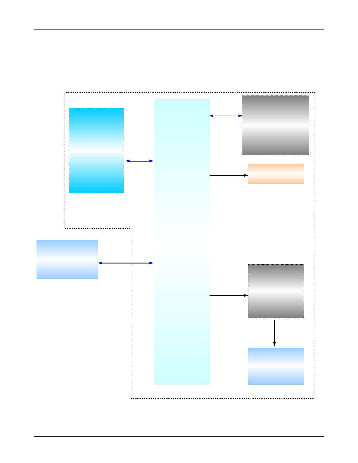
Base Band Solution Block Diagram
7-2.
MEMORY
Nor/UtRAM
K5N2866ATB-
(
AT80)
128/64
MB
PNX4902
Block Diagrams
LCD
1.77"
SDI
STN-LCD
Battery
mA
800
Elentec
RF/IF
Tranceiver
PMU
IIC
Interface/RTC
Basic Charging
SIM Interface
KEY PAD
AUDIO MIC
---------------
Ear MIC
Charging Controller
7-2
SAMSUNG Proprietary-Contents may change without notice
This Document can not be used without Samsung's authorization
SP
K
EARSPK
&

PCB Diagrams
8.
Top
0
3
1
C
3
0
1
T
N
A
MT207
C
C
C
C
C
C
C
C
C
4
4
4
4
4
0
1
0
1
1
1
2
0
1
R
5
0
2
T
M
ZD200
0
0
A
2
T
4
0
4
6
2
2
C
C227
T
8
M
1
2
Y
C
3
2
.
3
0
4
3
5
C
2
0
6
3
4
C420
1
4
5
C
I
R
M
U
4
HDC400
C
4
4
4
4
4
1
1
1
1
1
5
6
7
8
9
4
0
2
T
M
BTC200
2
0
4
R401
8
0
9
1
0
4
4
C
C
1
3
2
C
C232
R214
SIM200
5
6
7
0
0
0
4
4
4
R
R
R
T
T
T
T
P
P
P
P
5
2
2
2
2
0
0
0
0
0
2
7
6
8
3
P
T
TP217
T
P
2
0
C
2
2
1
9
1
2
C
1
0
2
P
T
2
0
2
P
T
1
1
L108
7
6
2
2
1
1
4
2
1
C
C
C
F
1
0
1
9
2
1
C
9
1
2
0
1
2
2
2
1
1
1
1
P
P
P
P
T
T
T
T
1
C
1
8
3
6
3
2
2
1
1
1
1
1
R
C
R
2
1
1
P
T
3
0
1
U
T
T
P
P
6
7
T
1
0
9
P
1
1
1
1
1
2
1
1
5
3
P
P
T
T
4
0
U
R201
2
0
2
C213
C212
8
5
T
P
0
1
P
T
U
M
I
C
4
5
1
1
3
1
TP113
6
P
5
T
-
0
2
.
8
Y
2
C
5
C118
1
2
1
C
C119
0
2
1
C
4
1
1
R
R115
C123
8
1
1
P
T
R
3
2
3
9
0
2
R
6
1
C205
C211
R207
0
0
2
T
H
O
S
C
2
0
2
2
C
1
C201
1
2
C
5
6
0
0
0
4
4
4
C
C
C
C407
C108
2
1
2
0
1
1
C
R
1
0
1
0
C
R
2
1
3
0
1
R
L
3
0
6
C
R
R306
3
3
1
1
4
5
3
0
3
R
R
3
2
2
1
0
U
3
8
0
2
C
0
2
5
R
2
0
3
U
0
0
2
C
S
O
2
C
C
2
3
2
2
2
2
C
R211
1
0
2
U
2
0
1
L
3
0
1
L
3
2
1
5
1
1
1
1
1
1
1
1
C
C
C
C
F100
R
F
S
1
0
1
C
L
1
1
0
0
0
7
6
1
1
C
R
2
3
4
0
0
0
4
4
4
C
C
C
3
0
2
R
5
7
L302
L301
C
3
2
3
R
3
0
5
6
0
2
R
Z
D
4
0
6
0
2
1
R
R
3
0
0
N
C
L
L300
3
0
3
3
0
1
C
1
0
U
1
Z
D
0
3
0
4
0
1
3
3
C
L
7
0
3
L
C
1
3
0
1
3
L
9
0
3
L
R
C
R
3
3
3
0
2
1
8
0
0
R
3
2
0
C
R
3
3
7
2
0
1
1
9
2
C
0
0
2
T
A
B
0
0
1
0
3
R
2
1
3
C
3
1
3
C
1
1
3
C
6
0
3
C
C
2
0
2
8
0
3
C
TP215
TP212TP213
TP216
TP214
TP219
1
0
0
C
R
1
1
0
0
1
6
0
2
3
C
Z
F
D
I
3
0
1
V
R
3
0
1
R
3
2
1
C325
T
3
A
R
3
4
0
0
0
3
R
C
3
1
0
7
0
3
1
C
0
2
A
T
C305
3
1
2
R
TP218
TP220
A
M
P
MT206
2
0
3
C
R210
3
0
3
2
C
0
3
8
C
0
2
R
1
1
3
R
C225
R316
C
C
2
2
0
1
4
0
C224
9
0
2
C
6
0
2
C
L
2
0
C
1
2
0
7
0
0
2
C
C214
TA202
L
2
2
1
0
0
0
2
2
2
D
D
C203
C110
0
0
1
A
T
L107
C117
1
1
1
R
8
0
1
R
C114
L104
MT208
9
0
3
C
MT203
C301
0
0
3
D
C304
D301
0
0
3
I
M
C
C100
5
4
0
0
1
1
C
C
2
0
1
T
N
A
0
1
1
N
T
A
2
0
2
T
M
8-1
SAMSUNG Proprietary-Contents may change without notice
This Document can not be used without Samsung's authorization
PCB Diagrams
Bottom
C
L
3
3
3
0
1
0
5
9
3
U
UP
S
E
N
D
DIGIT400
DIGIT403
L
E
F
T
LED402
L
E
D
4
0
0
INT
DOWN
DIGIT401
DIGIT404
R
I
G
H
T
LED403
L
E
D
4
0
1
SOFT400SOFT401
E
N
D
DIGIT402
DIGIT405
DIGIT406
S
T
A
R
DIGIT407
L
E
D
4
0
4
DIGIT409
L
E
D
4
0
5
DIGIT408
S
H
A
R
P
8-2
SAMSUNG Proprietary-Contents may change without notice
This Document can not be used without Samsung's authorization
 Loading...