

Page 1
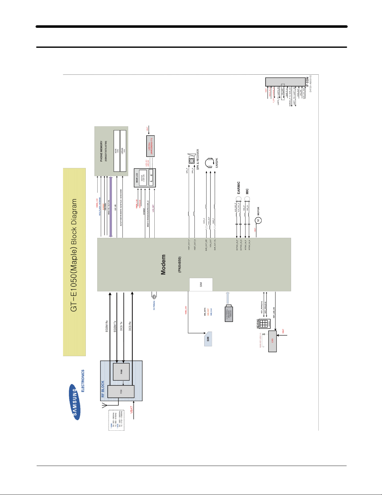
Level
8.
Block Diagram
8-1.
Repair
3
8-2
SAMSUNG Proprietary-Contents may change without notice
This Document can not be used without Samsung's authorization
Page 2
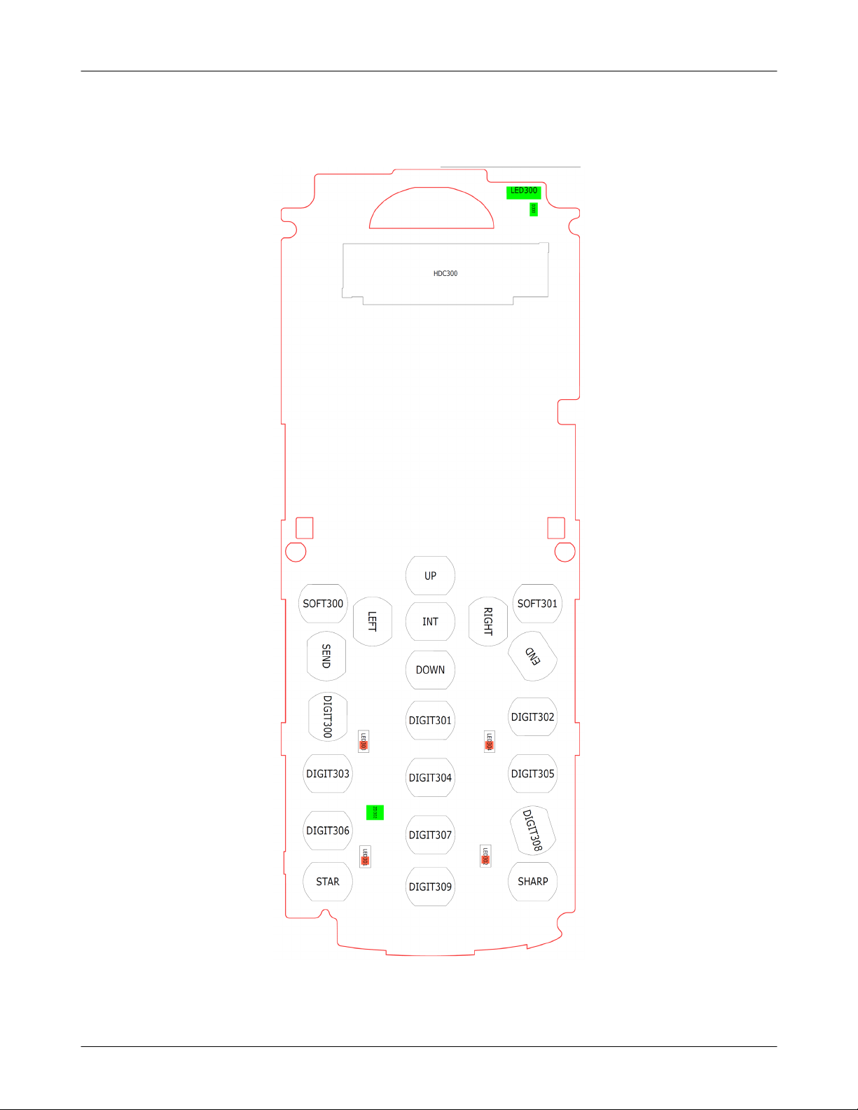
Level3Repair
PCB Diagrams
8-2.
8-2-1.
Top
(2010.12.01
Rev0.6)
8-2
SAMSUNG Proprietary-Contents may change without notice
This Document can not be used without Samsung's authorization
Page 3
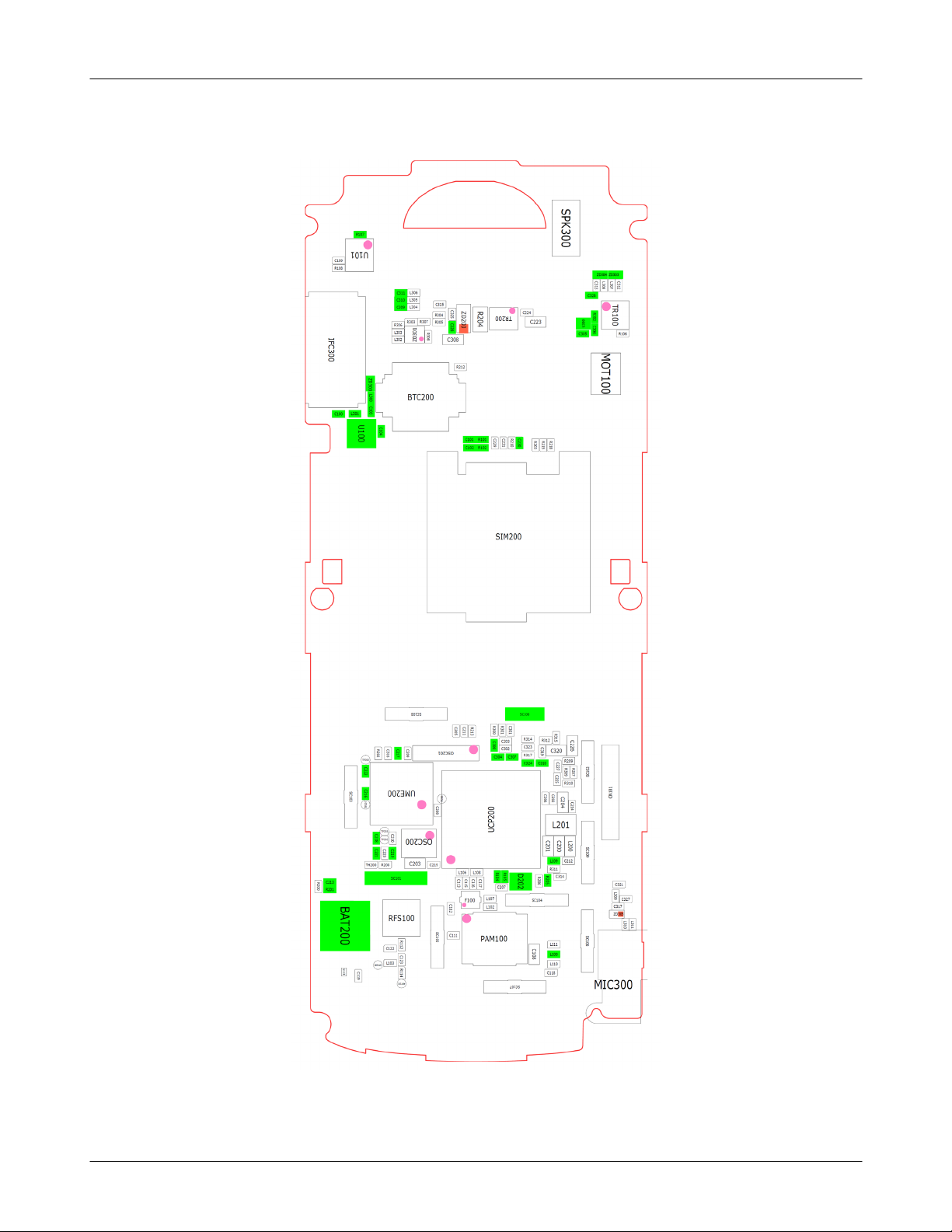
Level3Repair
8-2-1.
Bottom
8-3
SAMSUNG Proprietary-Contents may change without notice
This Document can not be used without Samsung's authorization
Page 4

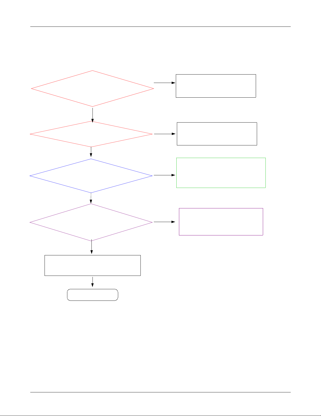
Level3Repair
Flow Chart of Troubleshooting
8-3.
presetting methods for checking TP
※
GND&TP(exp. VBUS_5.0V=
-
look over the coming out signal.
-
C594~
C599) using Oscilloscope
GND
Oscilloscope
←
TP(Test Point)
8-4
SAMSUNG Proprietary-Contents may change without notice
This Document can not be used without Samsung's authorization
Page 5
Level3Repair
8-3-1.
Power On
Check the Battery Voltage
is more than
TP:C108, C109, C212,C308)
(
PMU_VIO
TP:C207, C315)
(
Check the Clock at
UCP200 L16pin
CLK32K)
(
TP:OSC201
(
=2.8
=32
3.7V
Yes
Yes
KHZ
)
Yes
V?
No
No
Change the Battery
Because of batt. power low)
(
Check the Main Chip related to
GPIO_2.8V(TP:C207, C315)
V
Check the Main Chip
OSC201/look over the waverform
(TP:
using the oscilloscope)
VCORE
+
TP:C204, C214, L201)
(
Check the initial operation
_1.25V
V?
=1.25
Power On"
"
END
Yes
Yes
No
Resolder C204, C214 and L201
to confirm coming out power V_core)
(
8-5
SAMSUNG Proprietary-Contents may change without notice
This Document can not be used without Samsung's authorization
Page 6
Level3Repair
S
P
K
3
C223
0
0
ZD303ZD304
C
C
L
L
3
3
3
3
0
0
1
1
8
7
3
2
C326
T
R
R
1
3
0
0
2
0
0
0
3
C
U
3
0
6
C305
R106
M
O
T
1
0
0
R107
U
1
0
1
C109
R108
L306
C311
L305
C310
C309
R306
I
F
C
3
0
0
L301
C100
U
1
0
0
L303
L302
Z
D
3
0
0
L
3
0
0
C
1
0
3
C
1
0
4
L304
R307
R303
1
0
3
D
Z
BTC200
C315
C
Z
R
3
D
2
2
5
R304
2
0
0
4
C
R305
0
2
2
8
R
3
0
8
C308
R212
C224
T
2
R
0
0
8
0
1
C
S
C
C
R
2
2
2
0
1
1
5
1
3
C
C
R
2
0
2
TP200
C
2
2
2
C
2
S
1
C
6
1
0
3
7
0
2
P
T
C
2
1
8
C
2
2
1
TH200
R
C213
2
0
0
R201
B
A
T
2
0
0
0
L
1
1
3
0
C
1
1
9
TP203
TP202
C
2
2
0
R208
1
T
N
A
2
3
1
1
7
6
0
0
C
2
1
0
C
2
1
9
SC101
RFS100
C122
L103
C
2
0
9
E
U
2
M
0
0
C203
R
1
1
2
C
1
2
3
R
1
1
4
N
1
0
T
1
A
2
C
1
S
0
O
6
0
2
P
T
C
2
0
8
C
2
S
O
C215
L106
L108
C
C
C
C
1
1
1
1
1
1
1
1
3
5
6
7
L107
F100
C
1
1
2
S
C
1
C111
0
5
L102
PAM100
R
R
3
3
0
0
0
1
C
C303
3
0
0
C302
C304 C307
0
0
2
P
C
U
R
R
1
1
0
0
4
5
C207
SC100
C
3
0
1
R314
C323
R317
C324
C318
R
3
1
5
R312
C
3
1
9
C
2
2
6
C320
C
R209
2
2
R
R
7
C
2
2
5
C
C
2
2
C
0
0
2
2
6
0
4
3
0
9
R310
2
2
0
0
1
7
C
S
1
0
1
N
C
2
1
4
C
L201
C
C
L
2
2
2
0
0
0
0
1
L109
SC104
C
1
0
8
R311
R
R
C314
2
2
0
0
5
6
L111
L100
L110
C118
D
2
0
2
7
0
1
C
S
C212
0
S
C
1
0
9
S
C
1
0
6
MIC300
C321
L
3
0
9
C317
ZD305
C327
L
L
3
3
1
1
1
0
8-6
SAMSUNG Proprietary-Contents may change without notice
This Document can not be used without Samsung's authorization
Page 7
Level3Repair
8-3-2.
Initial
Initial Failure
Yes
UCP200 pin T4(RSTON)
="H(>2.4V)"?
TP106)
using the oscilloscope GND&TP
(TP:
Yes
CP200pin M4 or D12=
U
"H(>2.4V)"?
TP:LCD PIN5)
(
Yes
Check the16bit data signal
memory(TP:TP200)
&
No
No
Replace UCP200, must be"H"
Change PBA
to check LCD PIN5)
(
END
Yes
8-7
SAMSUNG Proprietary-Contents may change without notice
This Document can not be used without Samsung's authorization
Page 8

Level3Repair
8-8
SAMSUNG Proprietary-Contents may change without notice
This Document can not be used without Samsung's authorization
Page 9

Level3Repair
8-3-3.
Charging Part
UCP200 pin V9(AUX_DET
Check the UCP200 pin R9
or R303="L"?
Yes
1.4V
≒
Yes
END
)
No
No
Resolder or Replace R303
Must be"L"
Resolder or Replace UCP200
be possible that it is not soldering well)
(
8-9
SAMSUNG Proprietary-Contents may change without notice
This Document can not be used without Samsung's authorization
Page 10

Level3Repair
8-3-3.
Sim Part
Yes
SIM
or R210
After Power ON,
Check SIMClk Signal on
pin3 of SIM
method:wiring pin3and checking
(
its waveform using an oscilloscope)
pin
200
= "H=3.0V" ?
Yes
200ina
1
few second
No
No
Resolder R210, C231
insert SIM card&access it,
then must be sim pin1 or R210="H"
Resolder or Replace SIM200 connector.
Because of not soldering well)
(
Yes
After SIM card insert,
SIM
method:wiring pin3and check
(
look over if it get damaged.)
(
pin2(SIM_RST)
200
"H=3.0V"?
its waveform using an
oscilloscope)
Yes
Check the SIM Card
Yes
END
=
No
Confirm an another PBA
8-10
SAMSUNG Proprietary-Contents may change without notice
This Document can not be used without Samsung's authorization
Page 11

Level3Repair
8-3-2.
Microphone Part
Microphone does not work
UCP200 pin U18="H=2.85V"
at Mic Active
TP:C226)
(
Check the MIC Connection
look over schematics about
(
schemetics.)
Yes
Yes
Yes
No
?
No
Resolder L309, R313, R312, R314, C319, C323,
Resolder or Replace UCP200
Because of not soldering well
(
U302, C321
not work if those is not connected.)
(
)
Check the MIC sample.
it be possible the problem
(
things)
Yes
END
No
Replace an another MIC
because of being possible the problem)
(
8-11
SAMSUNG Proprietary-Contents may change without notice
This Document can not be used without Samsung's authorization
Page 12

Level3Repair
8-3-2.
Speaker Part
(
checking an waveform using
Speaker does not work
Yes
UCP200 pin W18, W19
>3.7V
Wiring the SPK N/P and
oscilloscope)
Yes
Does not work Voice call
?
Yes
No
No
Resolder C227 AND R209
be possible because of soldering not well)
(
Resolder or Replace UCP200
be possible of soldering not well or being
(
UCPabad sample)
Does not work Ringtone?
Menu->settings->profiles
(
options->Edit->
->
select the Call ringtone)
Yes
Is Speaker working?
Listening through the
(
speaker)
Yes
END
No
No
Resolder or Replace UCP200, SPK300
be possible of soldering not well or being
(
UCPabad sample)
Change Speaker ASS'Y
be possible of SPK Problems
(
or not inserting it right.)
8-12
SAMSUNG Proprietary-Contents may change without notice
This Document can not be used without Samsung's authorization
Page 13

Level3Repair
8-3-2.
Key Data Input
Check Initial Operation
When you pushed all of the
Key, does the key have
tension?
Yes
Yes
No
(#1 :
#2 :
whether be sunken
look over the Dome location
whether be out of line)
Change Domesheet
look over the Dome situation
All of the key doesn't work
except POWER ON KEY
No
END
Yes
?
because of be possible for PBA to get damaged)
Replace the PBA
over the insturctions again
(
and change the board
8-13
SAMSUNG Proprietary-Contents may change without notice
This Document can not be used without Samsung's authorization
Page 14

Level3Repair
8-3-2.
Back Light(for Color Main LCD)
Is LCD Contrast set on high
level in the Menu?
menu->settings->display-
(
Is U101 pin
Wiring pin
(
light->
>
LCD contrast)
Yes
H>2.7V"
1="
LCD_BL_EN)
#1/
?
No
No
Set LCD Contrast on high level
menu->settings->display->light
(
LCD contrast/select5Level(level
->
Resolder U101
#1 :
with an soldering iron)
(
Repalce LCD Module
#2 :
to check if it has the problem)
(
:1~5)
END
Yes
8-14
SAMSUNG Proprietary-Contents may change without notice
This Document can not be used without Samsung's authorization
Page 15

Level3Repair
8-3-2.
Key Back Light
UCP200 pin T8, V8
Wiring POWER ONKEY_1,
(
look over using an
Key LED does not work?
look over the LED light)
(
H=3.0V
"
GND
&
Yes
"?
Yes
=
2
No
No
Resolder or Replace UCP200
must be coming out the signal"H")
(
Replace the LED
be possible that the sample has the problem)
(
#1 :
#2 :
Change PBA
END
Yes
8-15
SAMSUNG Proprietary-Contents may change without notice
This Document can not be used without Samsung's authorization
Page 16

Level3Repair
presetting
※
Rx setting)
(
8960
Active Cell
1.
select GSM or GPRS
:
Connetion Type
2.
select Auto(GSM), BLER(GPRS)
:
BCH Parameter
3.
select measuring band(DCS or EGSM)
:
Cell power
4.
dBm
:-60
Tx setting)
(
After setting
※
After setting, prepare the call setup Display
1.
Using an Originate Call, makeacall.
2.
Confirm the display"connected"
3.
start the measuring
4.
8960 (
EGSM/DCS
)
8-16
SAMSUNG Proprietary-Contents may change without notice
This Document can not be used without Samsung's authorization
Page 17

Level3Repair
8-3-2.
GSM900 Receiver
Yes
PAM100
PAM100 Pin17
pin
pin G1
pin F1
Pin
dBm
-65
Yes
dBm
-68
Yes
F10
0
7,6≥-70
UCP
201
-70
≥
-70
≥
15
Yes
dBm
dBm
≥
≥
dBm
No
No
No
No
Resolder L110,L111,C118
Check PAM100 pin
Resolder F100
Resolder
=L
L108,C116,C117
8
Yes
No
Check ANT Switch
control circuit
Resolder PAM100
Yes
Check&Resolder
C200, C201, C203, C204,
And PMU Part and UCP201
L200,
Yes
END
8-17
SAMSUNG Proprietary-Contents may change without notice
This Document can not be used without Samsung's authorization
Page 18

Level3Repair
8-3-2.
DCS Receiver
Yes
PAM100
PAM100 Pin18
pin8,
pin E1
pin D1
dBm
-65
dBm
-68
F10
9≥-70
UCP
201
≥
≥
Pin
0
-70
-70
Yes
Yes
Yes
15
dBm
dBm
dBm
≥
≥
No
No
No
No
Resolder L110,L111,C118
Check PAM100
pin8=L,
Resolder F100
Resolder L106, C113,C115
10 =H
Yes
No
Check ANT Switch
control circuit
Resolder PAM100
Yes
Check&Resolder
C200, C201, C203, C204,
And PMU Part and UCP201
L200,
Yes
END
8-18
SAMSUNG Proprietary-Contents may change without notice
This Document can not be used without Samsung's authorization
Page 19

Level3Repair
R
0
0
F
S
1
C
G
G
A
1
2
3
4
PON_PA
BAND_SEL
2
3
1
C
4
1
1
R
1
1
2
0
1
1
L
8
1
1
C
L
1
0
0
L
1
1
1
R
L
1
0
3
2
2
1
C
1
0
1
T
N
A
3
1
1
L
9
1
1
C
X
S
G
R
M
E
D
S
C
R
X
N
A
RX_SEL
0
0
1
T
V
B
A
T
8
0
C
1
22
8
11
7910
24
GND
GND
4
1
D
N
G
5
1
N
A
T
0
2
N
G
D
6
1
C
N
GND
TX_EN
VBATT
VRAMP
GPCTRL0
GPCTRL1
PAM100
NC
GND3GND
GND
GND
GND
NC
RX018RX1
5
6
1
12
13
19
17
R
M
A
P
21
23
GND
4
B
R
I
_
F
L
N
2
F
R
I
N
B
_
H
1
1
1
C
X
M
E
T
S
G
_
D
C
X
_
T
S
2
1
1
C
F100
DCSRX
EGSMRX
N
P
T
O
I
O
0
K
h
:
m
1
O
EUR
0
0
2
:
N
,
R
C
:
,
R
0
N
2
C
0
I
N
H
A
C
:
USE
N
2
0
V
_
I
4
1
4
B
R
:
0
0
A
2
T
B
C
.
N
:
0
,
m
2
0
R
h
O
K
7
.
2
:
2
0
2
R
F
0
n
0
1
:
3
1
2
C
G
N
E
1
0
N
2
R
P
O
S
1
2
2
0
T
0
A
B
)
3
(
2
A
)
3
(
A
1
)
4
(
1
A
)
5
(
A
1
)
2
2
:
7
(
A
1
)
7
1
(
A
)
8
1
(
A
)
9
1
(
A
)
0
2
(
A
)
1
(
A
2
)
2
(
A
2
)
5
:
1
0
(
D
M
)
(
D
0
M
)
(
D
1
M
(
D
2
M
)
)
(
D
3
M
)
(
D
4
M
)
5
(
D
M
)
(
D
6
M
(
D
7
M
)
)
(
D
8
M
)
(
D
9
M
(
D
1
)
M
0
)
1
(
D
1
M
)
2
(
D
1
M
3
1
)
(
D
M
)
4
(
D
1
M
)
5
(
D
1
M
R
T
S
_
F
M
N
E
_
C
H
R
O
T
S
L
C
_
F
M
S
F
A
D
_
M
T
N
_
I
M
F
N
E
B
_
I
V
2
0
2
D
3
O
N
I
G
J
_
2
1
0
2
6
V
5
8
2
.
_
A
A
N
V
0
0
2
H
T
NCP15WB473J04RC
8
0
2
R
R
N
A
E
_
R
P
_
A
E
R
7
0
2
R
N
P
S
_
K
P
P
S
_
K
B
I
I
_
M
C
S
A
N
I
_
M
C
P
_
I
M
C
E
A
_
R
I
_
M
C
N
P
E
I
_
M
C
A
_
R
7
2
C
2
9
0
2
R
E
K
)
:
I
Y
2
N
0
(
E
)
:
I
Y
2
O
0
(
K
T
)
U
:
O
(
3
0
E
K
Y
L102
L107
B
V
T
A
V
P
V
.
R
0
E
_
3
M
0
0
2
R
C
3
C
2
1
L
F
M
_
F
R
M
_
5
2
2
C
6
2
2
C
S
A
E
W
_
R
F
E
E
R
A
R
_
S
_
W
)
I
(
N
0
K
E
Y
K
E
)
I
Y
(
N
1
K
E
)
I
Y
(
N
2
K
E
)
I
Y
(
O
0
K
E
)
I
Y
(
O
1
K
E
)
I
Y
(
O
2
)
(
0
E
K
Y
T
U
O
E
K
U
)
O
Y
T
(
1
E
K
U
)
O
Y
T
(
2
U
)
T
(
3
E
K
O
Y
L200
0
0
2
C
1
0
2
C
T11
R12
R13
VBAT_ANA
VBAT_ANA
VBAT_DCDC
2
G
1
ADD
R
1
4
1
E
ADD
R
2
6
1
E
ADD
R
3
6
1
F
ADD
R
4
1
1
E
ADD
R
5
0
1
E
ADD
R
6
0
D
1
ADD
R
7
0
1
B
ADD
R
8
9
E
ADD
R
9
D
9
0
ADD
R
1
1
G
1
1
ADD
R
1
3
D
1
2
ADD
R
1
4
D
1
3
ADD
R
1
T
A
#
I
W
-
R
/
Y
D
R
-
F
*
6
1
A
4
ADD
R
1
K
*
L
C
3
1
B
5
ADD
R
1
D
#
V
A
*
0
1
A
6
ADD
R
1
6
D
1
7
ADD
R
1
5
1
F
8
D
R
1
A
D
5
1
E
9
ADD
R
1
5
G
1
0
ADD
R
2
6
1
B
1
ADD
R
2
4
1
B
2
ADD
R
2
8
G
1
0
A
DAT
9
1
F
1
A
DAT
9
1
E
2
A
DAT
9
D
1
3
A
DAT
9
C
1
4
A
DAT
9
1
B
5
A
DAT
7
1
A
6
A
DAT
8
1
A
7
A
DAT
9
G
1
8
A
DAT
8
1
F
9
A
DAT
8
E
1
0
1
A
DAT
8
D
1
1
A
1
DAT
7
1
B
2
A
1
DAT
8
1
B
3
A
1
DAT
9
1
A
4
A
1
DAT
8
C
1
5
A
1
DAT
4
W
G
P
IO1
V
2
G
P
IO2
2
W
G
P
IO5
V
3
G
O
P
I
6
V
4
G
P
IO7
G
4
G
P
IO8
H
5
0
G
P
IO1
3
W
0
G
P
IO2
H
4
8
G
P
IO3
J
1
9
IO3
G
P
1
W
0
G
P
IO4
V
1
1
G
P
IO4
J
2
2
G
P
IO5
J
4
7
G
P
IO5
R
8
O
P
K
_
AUX
9
1
M
0
ADC
_
_
AUX
8
P
1
L
N
_
I
AUD
AUX
_
8
R
1
R
N
_
I
AUD
AUX
_
6
1
W
R
N
|
O
_
U
AR_
T
E
7
1
W
L
P
|
O
_
U
AR_
T
E
8
1
T
S
A
I
B
C
_
I
M
N
T
I
9
U
1
N
N
_
I
C
_
M
N
T
I
I
9
V
1
P
N
_
I
C
_
I
M
N
T
I
8
U
1
A
S
B
I
M
C
X
T
_
E
I
9
R
1
N
IN_
C
_
I
M
X
T
E
9
1
T
P
N
_
I
M
C
X
T
_
E
I
8
1
W
N
O
_
U
T
_
T
HSE
9
1
W
P
O
_
U
T
_
T
HSE
9
P
1
1
DET
_
W
HKS
9
N
1
2
DET
_
W
HKS
1
K
N
0
I
E
Y
K
2
K
N
1
I
E
Y
K
4
K
N
2
I
E
Y
K
1
L
IO0
E
Y
K
2
L
IO1
E
Y
K
4
L
IO2
E
Y
K
1
M
O
E
Y
0
K
U
T
2
M
O
E
Y
1
K
U
T
N
1
O
E
Y
2
K
U
T
N
2
Y
O
3
K
E
U
T
GND_GDGPA
GND_GDGPA
GND_GDGPA
GND_RFB3GND_RF
GND_AUD_DRV
GND_AUD_DRV
GND_AUD_DRV
GND_AUD
GND_RF
R6
B2
A3
T13
T14
T15
V18
H15
M15
B
9
OUT1
1
IN1
8
OUT1
7
OUT2
4
IN2
6
OUT2
G
G
G
G
5
3
2
0
1
V
5
.
2
1
R
_
E
V
O
C
V
.
8
1
E
M
_
V
M
A
B
T
V
VBG
V
5
.
V
8
2
N
A
_
A
V
.
R
V
8
5
F
2
B
V
R9
T12
M18
VBAT_RTC
VBAT_DCDC
_
T
A
T9
F4
K7
G5
B4
A4
V12
P16
VBG
VBAT_SENSE
K16
A15
A13
A14
R14
R15
R16
N15
VCORE
VDD_RF
VDD_RF
VDD_RF
VDD_GPPM
VDD_RF_IO
VDD_GPPM
VDD_VMEM
VDD_VMEM
VDD_RFDIG
VDD_AUDIO
VDD_VMEM1
VDD_AUDIO_DRV
VDD_AUDIO_DRV
U
P
X
N
GND_RF
GND_RF
GND_SUB
GND_RFE5GND_RFE6GND_RFE7GND_RF
GND_RFD4GND_RF
GND_RF
D2
C2
A
GND_RF
GND_RFD5GND_RFD6GND_RFD7GND_RF
GND_RF
GND_RF
F2
F5
H1
H2
E4
G2
E2
T10
T16
A
N
S
D
E
B
C113
C115
C116
C117
V
V
E
P
_
.
M
R
0
3
V
5
.
2
C
V
1
E
R
O
_
L7
K8
K10
K11
K12
K13
VDD_VCORE
VDD_VCORE
VDD_VCORE
VDD_VCORE
VDD_VCORE
VDD_VCOREL8VDD_VCOREL9VDD_VCOREK9VDD_VCORE
P
C
2
0
0
4
8
5
0
E
GND_VCOREG8GND_VCOREG9GND_VCORE
GND_VBAT_SNS
GND_VCORE
GND_VBG
GND_VCORE
GND_VCORE
GND_VCORE
E8
G7
D8
B9
A9
P15
2
1
2
R
K5
M7
L10
L11
L12
L13
M10
M11
M12
M13
NC
VDD_VCORE
VDD_VCORE
VDD_VCORE
VDD_VCORE
VDD_VCORE
VDD_VCORE
VDD_VCORE
VDD_VCORE
VDD_VCOREM8VDD_VCOREM9VDD_VCORE
T
GND_VCOREJ8GND_VCOREJ9GND_VCORE
GND_VCORE
GND_VCORE
GND_VCORE
GND_VCORE
GND_VCORE
GND_VCORE
GND_VCOREH8GND_VCOREH9GND_VCORE
J7
H7
J10
J11
J12
H10
H11
H12
G10
DCSRX_P
L106
DCSRX_N
EGSMRX_P
L108
EGSMRX_N
V
V
.
V
.
_
0
A
V
P
J5
P5
R5
N5
D15
B15
VDD_VIO
VDD_VIO
VDD_VIO
VDD_VIO
VDD_VIO2
VDD_VMEM
VDD_VMEM
PMU_LDO
GND_VCORE
GND_VCORE
GND_VCORE
GND_VCORE
GND_VCORE
GND_VCORE
L5
N7
N8
N9
M5
J13
2
C
V13
H13
VDD_VSIM
VDD_VPERM
1
D
1
N
0
B
E
2
E
1
N
1
B
E
2
A
1
N
CS0
2
B
1
N
CS1
1
A
1
N
CS2
J15
0
R
C
L
T
_
E
F
J16
1
R
C
L
T
_
E
F
5
K
1
2
R
C
L
T
E
_
F
5
1
L
3
R
C
L
T
E
_
F
5
1
W
P
M
V
I
U
_
O
4
1
W
M
P
V
ANA
U
_
5
V
1
M
M
P
V
M
U
_
E
2
1
W
R
M
E
P
M
V
P
U
_
3
1
W
M
P
VRF
U
_
4
V
1
M
M
I
P
V
S
U
_
8
T
N
I
P
O
K
_
V
8
O
U
_
T
K
P
O
7
T
M_O
0
W
U
T
P
5
T
1
T
M_O
W
U
P
6
T
M_O
2
W
U
T
P
8
W
ICH
G
N
9
W
C
H
I
G
P
E
1
N
D
_
I
R
F
D
1
P
D
_
I
R
F
G
1
N
E
_
I
R
F
1
F
P
_
E
I
R
F
1
A
R
FOH
2
A
R
FOL
8
1
L
R
D
_
0
UAR
T
8
K
1
D
T
_
0
UAR
T
5
W
D
R
_
1
UAR
T
V
5
D
T
_
1
UAR
T
V
7
S
C
T
_
1
UAR
T
6
W
S
R
T
_
1
UAR
T
7
A
1
6M_
2
_
L
A
X
T
6
A
2
_
M
6
2
_
L
A
X
T
9
1
L
1
_
K
2
3
_
L
A
T
X
9
K
1
2
K
_
2
3
_
L
A
T
X
5
A
D
SHL
_
A
L
T
X
8
B
D
SHL
_
A
L
T
X
7
B
D
SHL
_
A
L
T
X
6
B
D
SHL
_
A
L
T
X
5
B
D
SHL
_
A
L
T
X
8
A
D
SHL
_
A
L
T
X
9
H
1
K
M_C
I
L
S
8
H
1
A
DAT
_
M
I
S
6
G
1
M_RST
S
I
1
T
K
C
L
_
I
S
S
U
1
A
DAT
_
I
S
S
U
2
O
U
_
T
S
I
S
R
1
0
L
S
E
_
I
S
S
2
T
2
L
S
E
_
I
S
S
9
V
N
I
_
DET
ACC
_
6
1
L
O
U
T
K
_
2
3
K
_
C
L
0
1
V
VCH
G
6
1
V
VCM
O
U
_
T
7
1
V
O
U
_
T
VCM
1
1
V
C
O
W
S
R
E
1
1
W
C
O
W
S
R
E
0
R
1
REG
_
E
G
A
T
0
1
W
S
W
_
G
E
T
A
2
D
1
O
U
_
T
N
E
T
RES
4
T
N
E
T
RES
M
4
RST
N
T
6
1
M
RAM
_
P
A
P
4
P
C
K
R
T
2
P
C
K
T
N
4
D
I
T
1
P
D
O
T
R
2
M
T
S
R
4
S
T
E
T
6
V
N
HER
M_I
T
7
W
N
D
E
O
L
_
3
1
E
N
O
E
1
1
B
E
0
N
W
B
1
N
C
C
1
N
C
6
H
1
N
C
8
J
1
N
C
J19
N
C
6
N
1
N
C
8
N
1
N
C
R
7
N
C
1
N
C
2
N
C
GND_VSIM
GND_VCORE
GND_VCORE
GND_VCORE
USB_DP
USB_DN
R11
N10
N11
N12
N13
G13
V
P
V
.
R
0
E
_
3
M
V
.
0
3
I
S
_
M
V
V
.
8
2
I
_
O
G
V
V
S
3
V
V
1
2
A
N
O
5
I
C
_
_
E
.
R
M
2
V
.
R
V
8
5
F
2
_
2
0
1005
5
0
2
C
3
0
4
0
2
2
C
C
E
U
LATOR
REG
T
A
V
L
NEA
G
O
R
B
L
B
U
S
C
N
0
S
C
N
S
F
A
H
L
M
A
R
S
C
N
E
S
L
X
R
_
_
E
S
L
B
N
A
D
A
P
N
O
P
_
V
.
V
8
P
2
G
I
_
O
V
5
.
A
8
2
A
N
_
V
V
.
8
1
E
M
_
V
M
3
V
_
.
0
R
E
V
M
P
5
.
V
8
V
F
2
R
_
V
S
.
0
I
_
3
M
V
E
2
Y
_
O
K
N
O
_
K
N
1
Y
E
I
C
N
G
H
I
C
P
G
H
D
S
C
N
X
R
_
D
S
C
P
X
R
_
N
_
E
S
X
G
R
M
P
X
R
_
M
S
G
E
T
C
_
X
S
D
T
E
_
X
M
S
G
T
D
A
U
T
_
R
0
D
R
A
U
T
_
R
0
D
R
A
U
T
_
R
1
T
D
A
U
T
_
R
1
T
S
A
U
T
R
1
C
_
T
S
R
T
_
R
1
A
U
1
0
S
O
2
C
3
4
1
2
K
L
S
C
I
_
M
A
S
D
T
I
_
M
A
S
S
R
T
I
_
M
V
.
8
P
2
G
V
I
_
O
5
0
R
2
E
N
_
L
B
D
C
_
L
E
D
X
U
T
_
A
I
T
3
K
z
_
H
D
2
I
G
P
_
G
H
C
V
T
U
O
V
_
M
C
.
2
V
V
1
R
O
5
C
_
E
1
0
2
L
_
G
H
C
R
G
E
S
W
_
G
H
C
S
S
Y
S
R
T
N
O
T
S
R
T
S
R
T
N
_
R
P
M
A
R
T
C
K
T
K
C
T
D
I
O
D
T
T
S
M
F
V
E
O
n
n
E
W
8
5
1
V
.
I
P
2
8
_
G
V
O
M
E
_
.
M
8
V
1005
1005
1005
0
8
2
C
6
0
7
2
0
C
C
2
0
0
C
S
O
2
5
5
0
0
0
0
6
2
M
7
4
3
1
2
R213
V
.
3
3
E
K
_
D
L
E
_
Y
8-19
SAMSUNG Proprietary-Contents may change without notice
This Document can not be used without Samsung's authorization
Page 20

Level3Repair
L
3
0
S
C
1
0
6
MIC300
9
C327
C317
ZD305
L
L
3
3
1
1
1
0
B
A
T
2
0
0
L
1
1
3
RFS100
R
1
1
2
C122
C
1
2
3
A
N
1
T
0
0
L103
R
C
1
1
9
1
1
4
A
0
N
1
1
T
C
1
1
2
S
C
1
C111
0
5
L102
PAM100
L107
F100
SC104
L111
C
1
0
L100
8
L110
C118
0
C
1
S
7
8-20
SAMSUNG Proprietary-Contents may change without notice
This Document can not be used without Samsung's authorization
Page 21

Level3Repair
8-3-2.
GSM900 Transmitter
TX ON(5Level)
Yes
30
dBm
Pin
dBm
No
15
≥
-4
≥
PAM100
PAM100 pin4
yes
Yes
Yes
Resolder L110, L111, C118
CheckPAM
pin
Pin
Check PAM100
VBATT(pin11) OK?
8=H
10 = H
Yes
100
Yes
No
Check ANT Switch
Change or ResolderPAM
Check UCP201
control circuit
100
No
UCP201 pinA2
dBm
-4
≥
No
Check&Resolder
C200, C201, C203, C204,
And PMU Part and UCP201
L200,
Yes
END
Yes
No
Resolder or Change
L105, C110, C111
Check VBAT or PAM
control signal
8-21
SAMSUNG Proprietary-Contents may change without notice
This Document can not be used without Samsung's authorization
Page 22

Level3Repair
8-3-2.
DCS Transmitter
TX ON(5Level)
Yes
30
dBm
Pin
dBm
15
No
2≥-4
PAM100
PAM100 pin
-Rx:
-Tx:
≥
yes
Yes
Yes
Resolder L110, L111, C118
CheckPAM
pin
Pin
Check PAM100
VBATT(pin11) OK?
4=H
5=H
Yes
100
Yes
No
Check ANT Switch
Change or ResolderPAM
Check UCP201
control circuit
100
No
UCP201 pinA1
dBm
-4
≥
No
Check&Resolder
C200, C201, C203, C204,
And PMU Part and UCP201
L200,
Yes
END
Yes
No
Resolder or Change
C112
Check VBAT or PAM
control signal
8-22
SAMSUNG Proprietary-Contents may change without notice
This Document can not be used without Samsung's authorization
Page 23

Service Schematics
8-4.
NC Point(Top View)
-
NC
:
UCP200
1 2 3 4 5 6 7 8 9 10111213141516171819
A
B
C
D
E
F
G
H
J
K
L
M
N
P
R
T
U
V
W
1 2 3 4 5 6 7 8 9 10111213141516171819
Level3Repair
A
B
C
D
E
F
G
H
J
K
L
M
N
P
R
T
U
V
W
8-23
SAMSUNG Proprietary-Contents may change without notice
This Document can not be used without Samsung's authorization
Page 24

Level3Repair
NC
:
UME200
12345678910
A
B
C
D
E
F
12345678910
A
B
C
D
E
F
8-24
SAMSUNG Proprietary-Contents may change without notice
This Document can not be used without Samsung's authorization
 Loading...