

Samsung Dvd-829 Circuit Descriptions
Samsung Electronics 6-1
6. Circuit Descriptions
6-1 S.M.P.S.
6-1-1 Comparsion between Linear Power Supply and S.M.P.S.
6-1-1 (a) Linear
Vreg
Vout
+
–
+
+
–
Vs
(Ns)
Vp
(Np)
REGULATOR
Common power
(Ex.120/220V 50/60Hz)
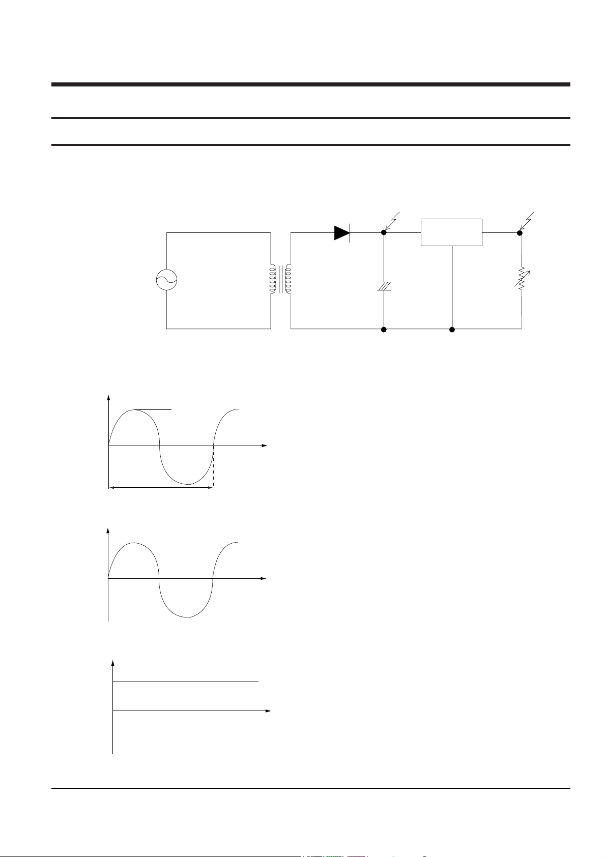
Fig. 6-1 Linear Power Supply
3 Waveform/Description
Vs
t
0
Fig. 6-2
Vs
t
0
Fig. 6-3
Vout
t
0
Fig. 6-4
Input : Common power to transformer (Vp).
The output Vs of transformer is determined by the ratio
of 1st Np and 2nd Ns.
Vs = (Ns/Np) x Vp
Vout is output (DC) by diode and condensor.
Circuit Descriptions
6-2 Samsung Electronics
3 Advantages and disadvantages of linear power supply
1) Advantages : Little noise because the output waveform
of transformer is sine wave.
2) Disadvantages :
ΠAdditional margin is required because Vs is chan-
ged (depending on power source). (The regulator
loss is caused by margin design).
´ Greater core size and condensor capacity are ne-
eded, because the transformer works on a single
power frequency.
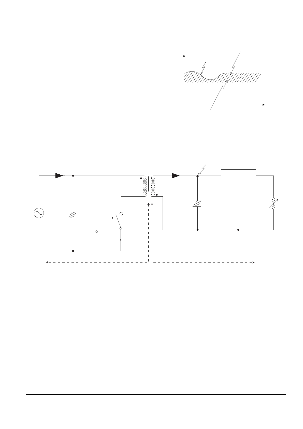
6-1-1 (b) S.M.P.S. (Pulse width modulation method)
v
Vreg
Vout
0
t
Change by common power
Regulator loss
Fig. 6-5
3 Terms
1) 1st : Common power input to 1st winding.
2) 2nd : Circuit followings output winding of transformer.
3) f (Frequency) : Switching frequency (T : Switching cycle)
4) Duty : (Ton/T) x 100
Transformer
Vout
(Np)
(Vp)
Switch
Vs switch
I switch
Vin
ON/OFF Control
+
–
+
–
+
+
+
–
(Vs)
(Ns)
REGULATOR
Fig. 6-6
Circuit Descriptions
Samsung Electronics 6-3
6-1-2 Circuit description (FLY-Back PWM (Plise Width Modulation) Control)
6-1-2 (a) AC Power Rectification/Smoothing Terminal
1) PD01,PD02,PD03,PD04 : Convert AC power to DC(Wave rectification)
2) PE3 : Smooth the voltage converted to DC(Refer to VIN of Fig. 6-7)
3) PC01, PC02, PC10, PC11, PC12, PC13, PL01, PL02, PL03 : Noise removal at power input/output
4) PVA1 : SMPS protection at power surge input (PVA1 pattern open is to remove noise)
5) PR10 : Rush current limit resistance at the moment of power cord insertion.
ΠRush current = (AC input voltage x 1.414 - Diode drop voltage) / Pattern resistance + PL02,01 resis-
tance + PC10 resistance + PR10) (AC230V based : approx. 26A)
´ Without PR10, the bridge diode might be damaged as the rush current increases.
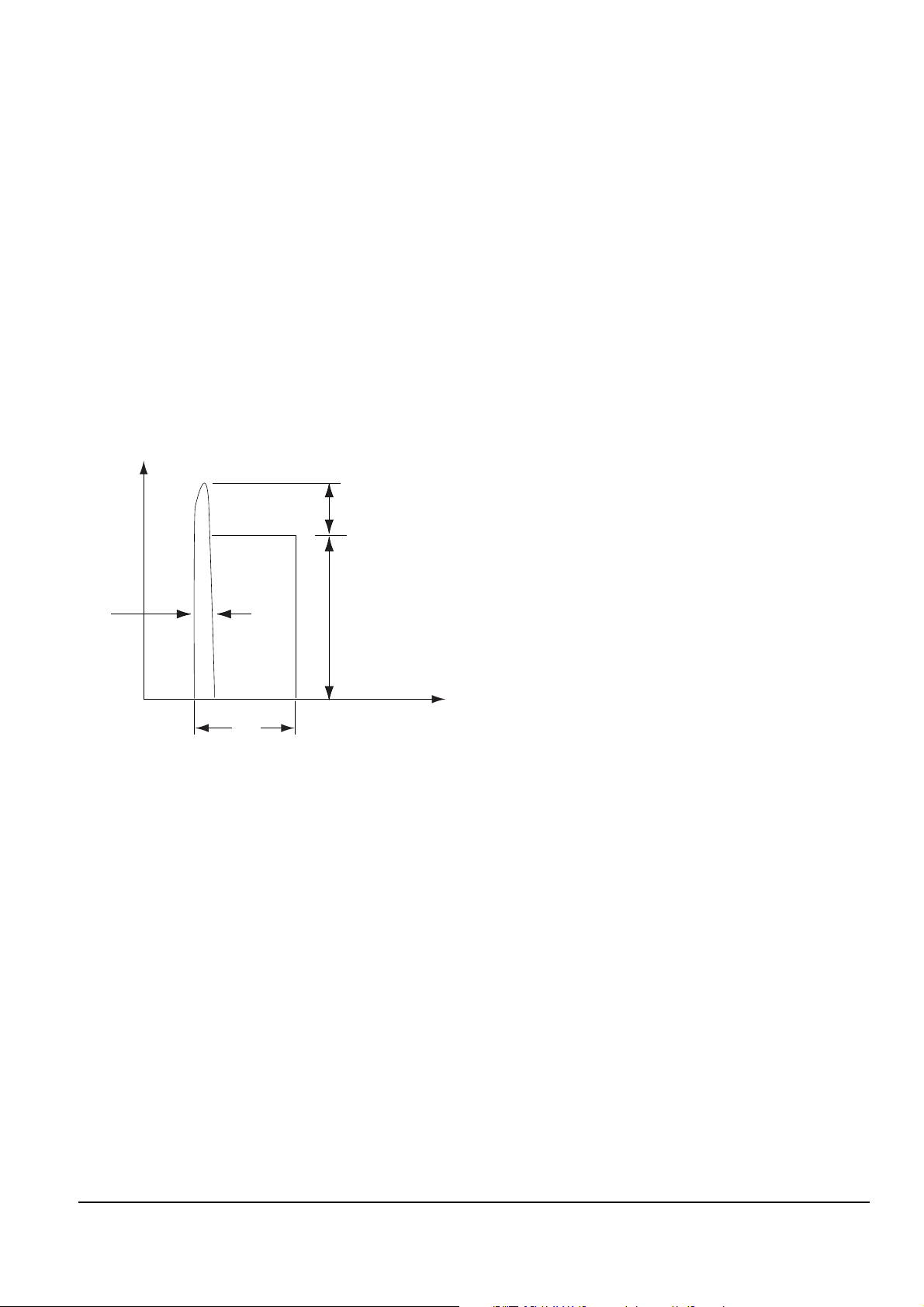
6-1-2 (b) SNUBBER Circuit : PR15, PR16, PC04, PC05, PD11, PR17
0
Vswitch
dt
Toff
t
Inverted power
by leakage
inductance
Fig. 6-7
1) Prevent residual high voltage at the terminals of
switch during switch off/Suppress noise.
High inverted power occurs at switch (PIC1) off,
because of the 1st winding of transformer :
(V= LI xdi/dt. LI : Leakage Induction)
A very high residual voltage exists on both terminals
of PIC1 because dt is a very short.
2) SNUBBER circuit protects PIC1 from damage
through leakage voltage suppression by RC,
(Charges the leakage voltage to PD11 and PC04, and
discharges to PR15 and PR16).
3) PC05, PR17 : For noise removal
6-1-2 (c) PIC1 Vcc circuit
1) PR11, PR12, PR13, PR14 : PIC1 driving resistance (PIC1 works through driving resistance at power cord in)
2) PIC1 Vcc : PR18, PD12, PE6
Œ
Use the output of transformer as Vcc, because the current starts to flow into transformer while PIC1 is active.
´ Rectify to PD12 and smooth to PE6.
ˇ Use the output of transformer as PIC1 Vcc : The loads are different before and after PIC1 driving.
(Vcc of PIC1 decreases below OFF voltage, using only the resistance due to load increase after PIC1 driving.)
Circuit Descriptions
6-4 Samsung Electronics
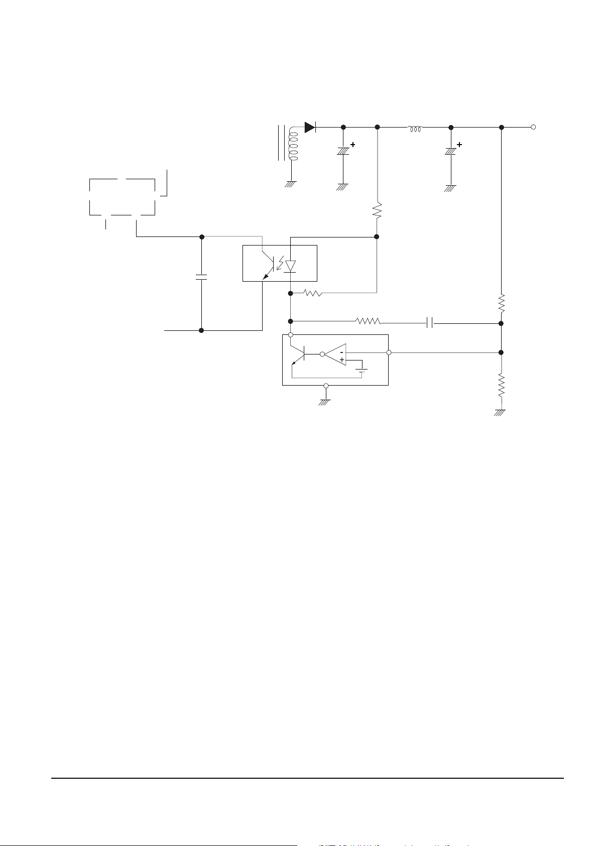
1) F/B terminal of PIC1 determines output duty cycle.
2) C-E(Collector-Emitter) of PIC2 and F/B potential of PIC1 are same.
3 Operation descriptions
1) Internal OP-Amp Ô+Õ base potential of PIC3 is 2.5V and external Ò-Ó input potential is connected with PR38 and
PR39 to maintain Vout of 5.8V. (Vout = ((PR36 x PR39) / PR39) x 2.5V)
2) If load of 5.8 V terminal increases(or AC input voltage decreases) and Vout decreases below 5.8V, then :
PIC3 ÔPÕ potential down below 2.5V --> PIC3 A-K of base current down --> PIC3 of A-K current down -->
PIC2 Diode current down --> PIC2 C-E current down --> PIC2 C-E voltage up --> PIC1 F/B voltage up -->
Out Duty up --> Transformer 1st current up --> Transformer 1st power up --> Vout up --> Maintain Vout 5.8V
3) If load of 5.8 V terminal decreases(or AC input voltage rises) and Vout rises above 5.8V, then :
Reverse sequence of the above description --> Duty down --> Vout down --> Maintain 5.8V (i.e., the feedback
to maintains 5.8V).
ΠPR35, PR36 : Reduce 5.8V overshoot
´ PR37, PC44 : Prevent PIC3 oscillation(for phase correction)
ˇ PC09 : Adjust feedback response rate
6-1-2 (d) Feedback Control Circuit
PIC1
STR-G6153T
OCP
DRAIN
F/B
PC09
PIC2
C
E
1st GND
A
K
PIC3
A
2.5V
K
P
PR36
PR37
PC44
2nd GND
PR38
PR39
PR35
PC34
5.8V
PL34
PD33
PE33
Trans
GND
%
! @
#
$
VCC
Fig. 6-8
Circuit Descriptions
Samsung Electronics 6-5
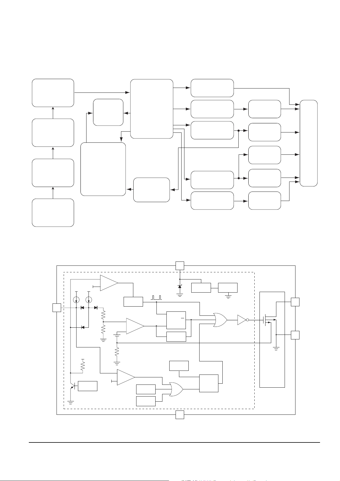
6-1-3 Internal Block Diagram
6-1-3 (a) Internal Block Diagram of S.M.P.S. Circuit
Smoothing
Circuit
Rectified Circuit
Line Filter
Power IN
(85~265V)
Noise
Removal
(SNUBBER)
PWM Control
Circuit
(1L0380)
Converter
Voltage
Detection
Circuit
FLT Driving
Circuit
3.3V Rectified
Smoothing Circuit
5V Rectified
Smoothing Circuit
8V Rectified
Smoothing Circuit
-8V Rectified
Smoothing Circuit
3.3V Rectified
VoltageCircuit
5V Rectified
VoltageCircuit (x2)
Motor 8V
1 Port
8V Rectified
VoltageCircuit
-8V Rectified
VoltageCircuit
O
U
T
P
U
T
Fig. 6-9
6-1-3 (b) PIC1 (STR-G6153T) Internal Block Diagram
Voltage
Ref.
UVLO
Vcc
Drain
Source
GND
Sense
S
Q
R
S
Q
R
OSC.
Vck
32V
Feedback
LEB
Reset
7.5V
5v
Reset
Thermal
Protection
OVP
2uA
6.3V
Sync.
2.5R
Voffset
Rsense
R
+
_
+
_
1mA
Control IC
Sense
FET
5
OCP
2
4
1
3
Fig. 6-10
Circuit Descriptions
6-6 Samsung Electronics
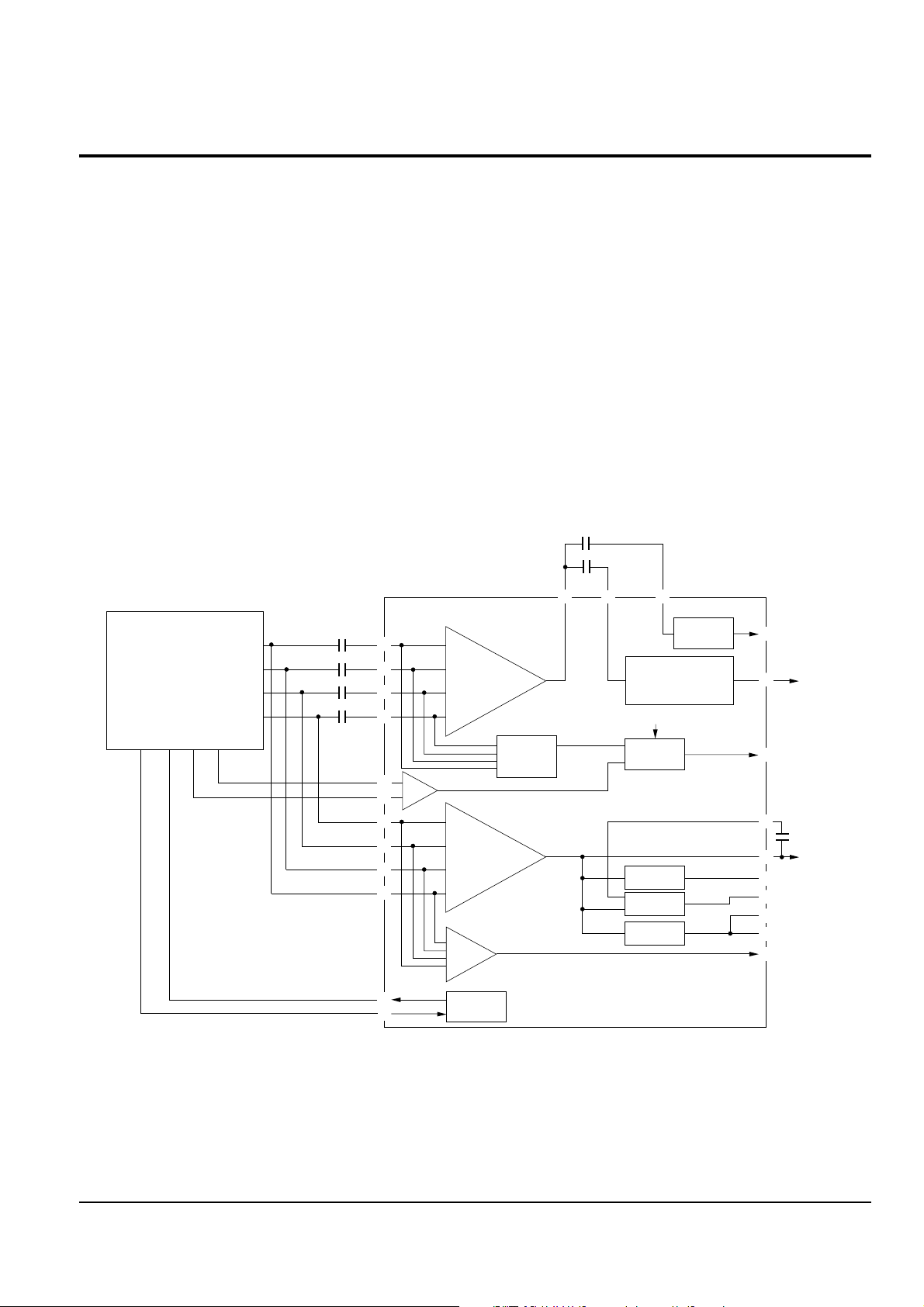
6-2 RF
6-2-1 RIC1 (KS1461)
KS1461 is combined with KS1452 and KS1453 as bipolar IC developed for DVD SERVO system.
Main features include DVD waveform equalizing, CD waveform equalizing, focus error signal generation, 3-beam
tracking error signal generation, DPD 1-beam tracking error, defect, envelope, MIRR output, etc. after receiving the
pick-up output converted into I/V.
6-2-1 (a) Basic Potentiometer
KS1461 uses a single power method and each circuit is based on V of 2.5V.
V (Pin 12, 20, 24, 67) terminal is needed for IC, which uses the peripheral V.
6-2-1(b) RF signal
Fig. 6-11 shows the flow of signal generated by the pick-up.
A, B, C, D signals detected from pick-up are converted in to RF signal(A+B+C+D) via RF summing AMP.
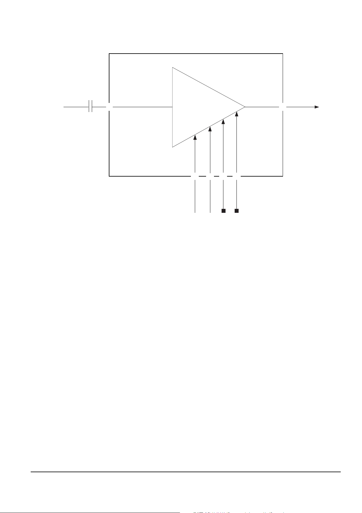
Fig. 6-12 shows the waveform-equalizing block diagram for the RF signal.
It outputs to EQout (Pin 86) terminal by initially changing switching AMP gain of DVD and CD, and then adjusting the level in RF SUM & AGC. It controls RF SUM & AGC gain by means of Pin 89-95 and interfaces with PWM
signal, (output from PWM terminal of KS1453, via low-pass filter to adjust boost gain and peak frequency.
EQout terminal is connected with EQin (Pin 86).
PICK-UP
RE SUM
& AGC
RF EG
DPD
TE
Mhx
ENV
FOK
DEFECT
TESEL
TE
ABCD
SUM
FE
ALPC
MIRR
%
^
&
*
5
6
7
8
3
4
104
104
104
104
? . m
474
104
RFAGCO EQIN
MIRRI
G
,
y
I
i
T
F
P
[
d
MIRR
TE
RFEQO
A
B
C
D
EFLDPD
w
E
ABCD
FE
DFCT1
DFCT2
FOKB
ENV
103
ABCDI
Fig. 6-11
Circuit Descriptions
Samsung Electronics 6-7
REAGCO
RFEQO
EQIN
474
RF EQ
PWM1
EQG
EQF
PLLGF
VZOCTL
PWM2
VREFEQ
RFDVCC
?
.
,
‡
°
·
‚
Fig. 6-12
The control parameters of DVD EQ and CD EQ are as follows.
1) DVD CD EQ control parameter
ΠEQG (Pin 97) : Changes the gain of peak frequency with EQ frequency characteristic. Convert PWM signal,
output from KS1453, into DC via low-pass filter.
´ EQF (Pin 98) : Changes the peak frequency with EQ frequency characteristic. Convert PWM signal, output
from KS1453, into DVD via low-pass filter.
 Loading...