

Samsung DVD-811, DVD-711 Circuit Descriptions
Samsung Electronics 5-1
5. Circuit Descriptions
5-1 Power (120/127 Voltage)
5-1-1 Comparsion between Linear Power Supply and S.M.P.S.
5-1-1 (a) Linear
Vreg
Vout
+
–
+
+
–
Vs
(Ns)
Vp
(Np)
REGULATOR
Common power
(Ex.120/127V 60Hz)
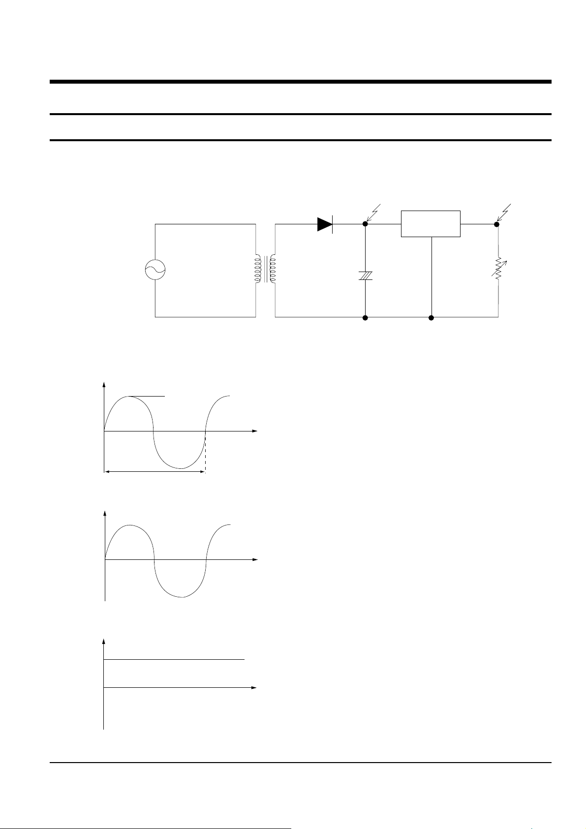
Fig. 5-1 Linear Power Supply
◆ Waveform/Description
Vs
t
0
Fig. 5-2
Vs
t
0
Fig. 5-3
Vout
t
0
Fig. 5-4
Input : Common power to transformer (Vp).
The output Vs of transformer is determined by the ratio
of 1st Np and 2nd Ns.
Vs = (Ns/Np) x Vp
Vout is output (DC) by diode and condensor.

Circuit Descriptions
5-2 Samsung Electronics
◆ Advantages and disadvantages of linear power supply
1) Advantages : Little noise because the output waveform
of transformer is sine wave.
2) Disadvantages :
ΠAdditional margin is required because Vs is chan-
ged (depending on power source). (The regulator
loss is caused by margin design).
´ Greater core size and condensor capacity are ne-
eded, because the transformer works on a single
power frequency.
5-1-1 (b) S.M.P.S. (Pulse width modulation method)
v
Vreg
Vout
0
t
Change by common power
Regulator loss
Fig. 5-5
◆ Terms
1) 1st : Common power input to 1st winding.
2) 2nd : Circuit followings output winding of transformer.
3) f (Frequency) : Switching frequency (T : Switching cycle)
4) Duty : (Ton/T) x 100
Transformer
Vout
(Np)
(Vp)
Switch
Vs switch
I switch
Vin
ON/OFF Control
+
–
+
–
+
+
+
–
(Vs)
(Ns)
REGULATOR
Fig. 5-6
Circuit Descriptions
Samsung Electronics 5-3
5-1-2 Circuit description (FLY-Back Control)
5-1-2 (a) AC Power Rectification/Smoothing Terminal
1) PDS01, PDS02, PDS03, PDS04 : Convert AC power to DC(Wave rectification).
2) PE3 : Smooth the voltage converted to DC.
3) PCR01, PCR02, PCD01, PCD02, PCD03, PLS01, PBS01 : Noise removal at power input/output.
4) PVA1 : SMPS protection at power surge input (PVA1 pattern open is to remove noise).
5-1-2 (b) SNUBBER Circuit : PER11, PDS11, PCR11, PCD12, PRS11, PRS12
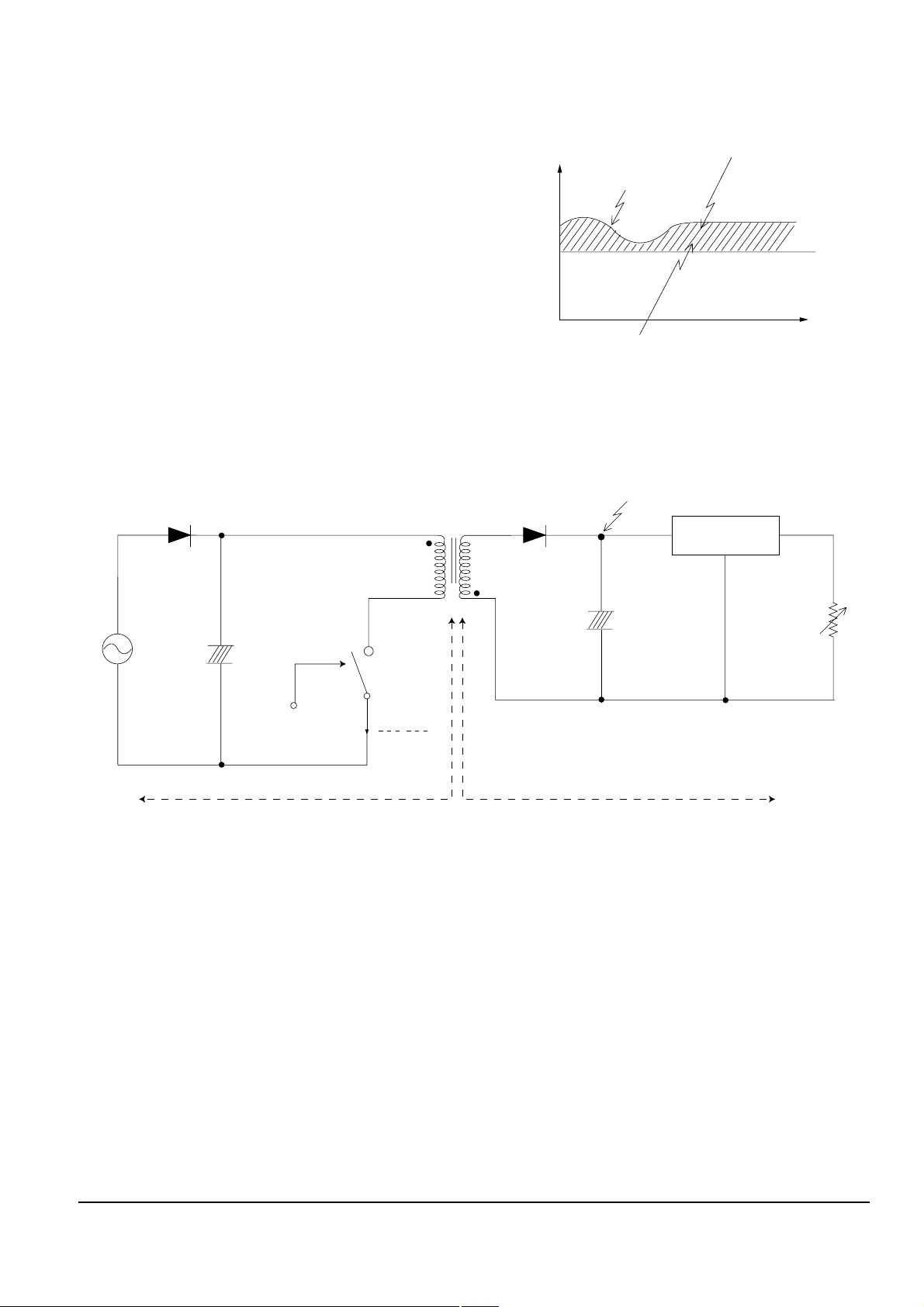
0
Vswitch
dt
Toff
t
Inverted power
by leakage
inductance
Fig. 5-7
1) Prevent residual high voltage at the terminals of
switch during switch off/Suppress noise.
High inverted power occurs at switch (PIC1) off,
because of the 1st winding of transformer :
(V= LI xdi/dt. LI : Leakage Induction)
A very high residual voltage exists on both terminals
of PQR11 because dt is a very short.
2) SNUBBER circuit protects PIC1 from damage
through leakage voltage suppression by RC,
(Charges the leakage voltage to PER11, PDS11, PCR11,
PCD12, and discharges to PR15 and PR16).
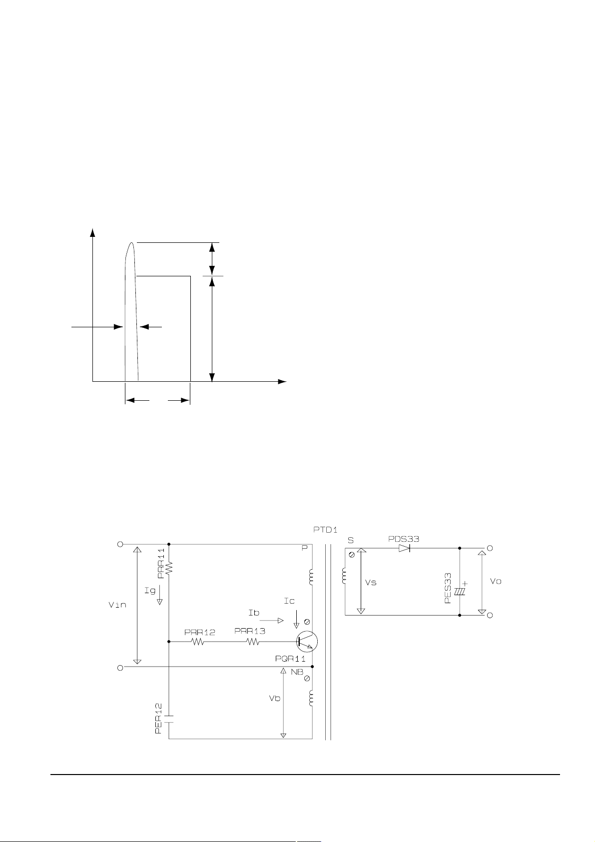
5-1-2 (c) Driving circuit
When Vin supplied, driving current Ig occurs throuhg the PRR11. By this IC (=HfexIg) occurs throug the PQR11
and the Vb is inducted to base winding coil NB of PQR11. By inducted Vb, Ib start flow and the PQR11 is saturated (S/W ON). Ib is constant and Ic increases in propotion to time. After constant time passed Ib become to
shotage and PQR11 is cut OFF (S/W OFF).
Fig. 5-8 Driving Circuit
Circuit Descriptions
5-4 Samsung Electronics
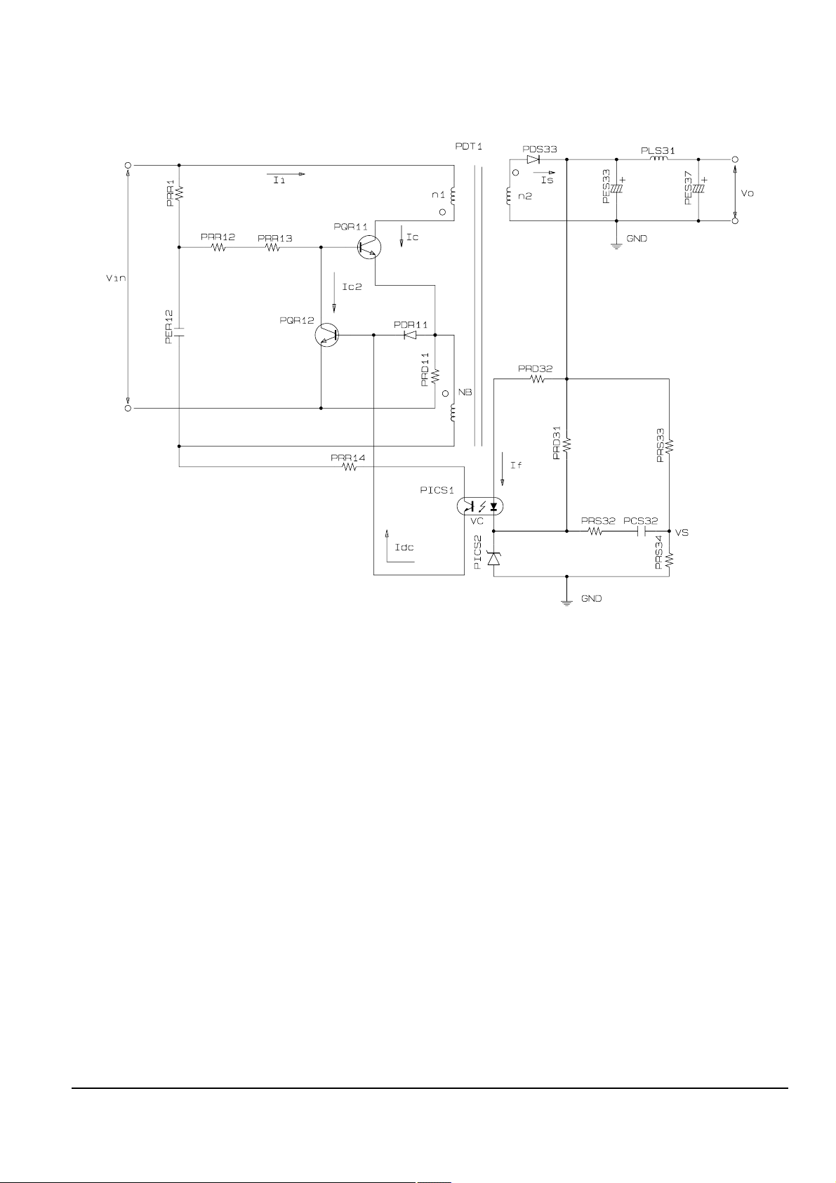
◆ Operation descriptions
1) Internal OP-Amp ‘+’ base potential of PICS2 is 2.5V and external “-” input potential is connected with PRS33
and PRS34 to maintain Vout of 5.8V.
2) If load of 5.8V terminal decreses (or AC inout voltage increases) and Vout increases over 5.8V,
Then : PICS2 Vs potential up over 2.5V --> PICS2 Vc down --> PICS1 A-K potential down --> PICS1 C-E current
up --> PQR12 base current up --> PQR11 base current down --> Vout down --> Maintain 5.8V
- PRD31, PRD32 : Reduce 5.8V overshoot.
- PRS32, PCS32 : Prevent PICS2 oscillation (for phase correction).
5-1-2 (d) Feedback Control Circuit
Fig. 5-9

Circuit Descriptions
Samsung Electronics 5-5
5-1-3 Internal Block Diagram
◆ Internal Block Diagram
Smoothing
Circuit
Rectified Circuit
Line Filter
Power IN
(120/127V)
Noise
Removal
(SNUBBER)
Power TR
Control Circuit
Converter
Voltage
Detection
Circuit
FLT Driving
Circuit
3.3V Rectified
Smoothing Circuit
5V Rectified
Smoothing Circuit
8V Rectified
Smoothing Circuit
-8V Rectified
Smoothing Circuit
3.3V Rectified
VoltageCircuit
5V Rectified
VoltageCircuit (x2)
Motor 8V
1 Port
8V Rectified
VoltageCircuit
-8V Rectified
VoltageCircuit
O
U
T
P
U
T
Fig. 5-10
Circuit Descriptions
5-6 Samsung Electronics
5-2 Power (Free Voltage)
5-2-1 Comparsion between Linear Power Supply and S.M.P.S.
5-2-1 (a) Linear
Vreg
Vout
+
–
+
+
–
Vs
(Ns)
Vp
(Np)
REGULATOR
Common power
(Ex.110~240V 50/60Hz)
Fig. 5-11 Linear Power Supply
◆ Waveform/Description
Vs
t
0
Fig. 5-12
Vs
t
0
Fig. 5-13
Vout
t
0
Fig. 5-14
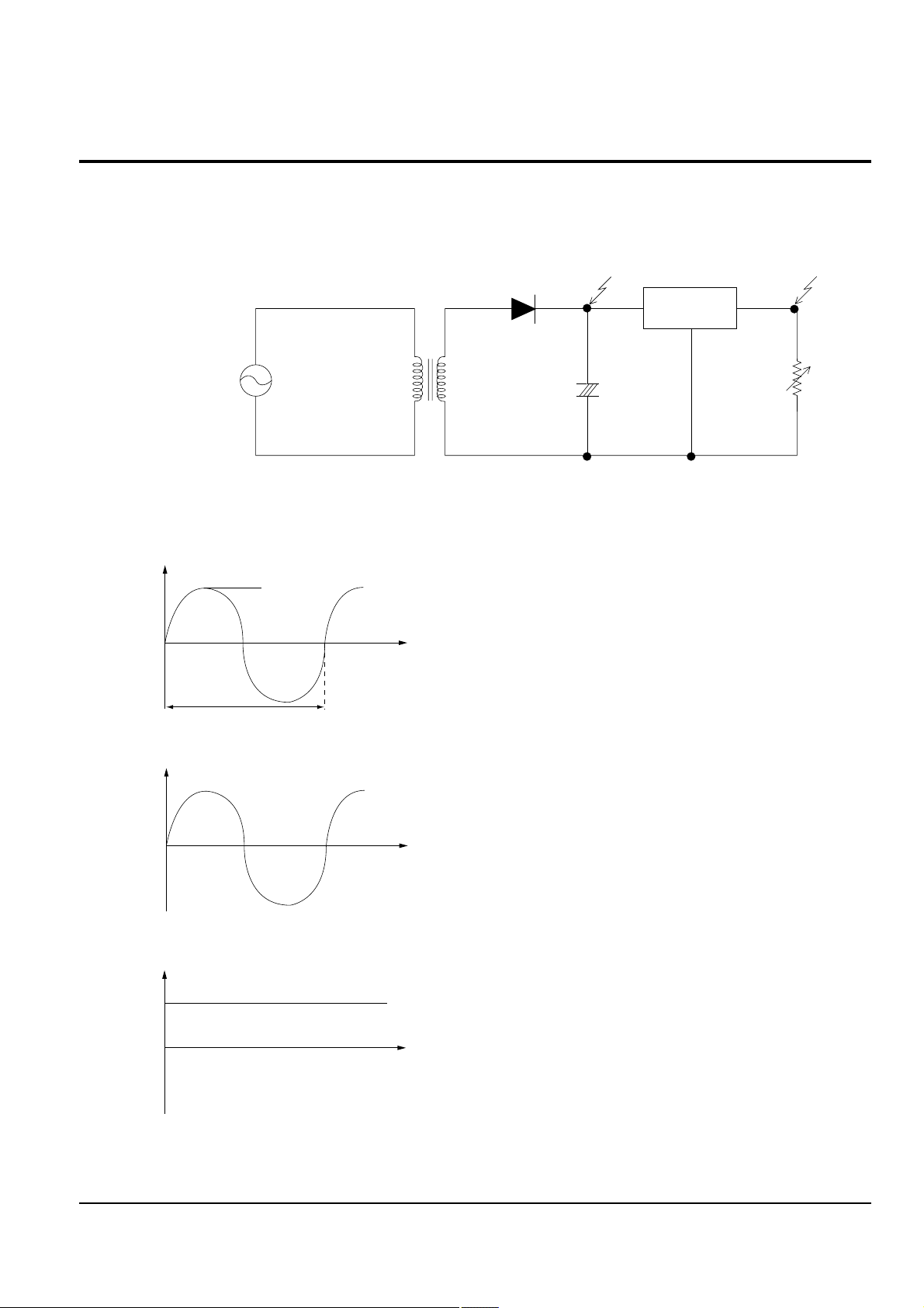
Input : Common power to transformer (Vp).
The output Vs of transformer is determined by the ratio
of 1st Np and 2nd Ns.
Vs = (Ns/Np) x Vp
Vout is output (DC) by diode and condensor.
Circuit Descriptions
Samsung Electronics 5-7
◆ Advantages and disadvantages of linear power supply
1) Advantages : Little noise because the output waveform
of transformer is sine wave.
2) Disadvantages :
ΠAdditional margin is required because Vs is chan-
ged (depending on power source). (The regulator
loss is caused by margin design).
´ Greater core size and condensor capacity are ne-
eded, because the transformer works on a single
power frequency.
5-2-1 (b) S.M.P.S. (Pulse width modulation method)
v
Vreg
Vout
0
t
Change by common power
Regulator loss
Fig. 5-15
◆ Terms
1) 1st : Common power input to 1st winding.
2) 2nd : Circuit followings output winding of transformer.
3) f (Frequency) : Switching frequency (T : Switching cycle)
4) Duty : (Ton/T) x 100
Transformer
Vout
(Np)
(Vp)
Switch
Vs switch
I switch
Vin
ON/OFF Control
+
–
+
–
+
+
+
–
(Vs)
(Ns)
REGULATOR
Fig. 5-16
Circuit Descriptions
5-8 Samsung Electronics
5-2-2 Circuit description (FLY-Back PWM (Plise Width Modulation) Control)
5-1-2 (a) AC Power Rectification/Smoothing Terminal
1) PDS01, PDS02, PDS03, PDS04 : Convert AC power to DC(Wave rectification)
2) PEF10 : Smooth the voltage converted to DC(Refer to VIN of Fig. 5-17)
3) PLF01, PLS01, PCF01, PCF02, PCD01, PCD03, PCS03 : Noise removal at power input/output
4) PVA1 : SMPS protection at power surge input (PVA1 pattern open is to remove noise)
5) PR10 : Rush current limit resistance at the moment of power cord insertion.
ΠRush current = (AC input voltage x 1.414 - Diode drop voltage) / Pattern resistance + PLF01, PLS01
resistance + PCD01 resistance + PRF10) (AC230V based : approx. 26A)
´ Without PRF10, the bridge diode might be damaged as the rush current increases.
5-2-2 (b) SNUBBER Circuit : PRS11, PRS12, PRD12, PCD12, PDS11, PCF11
0
Vswitch
dt
Toff
t
Inverted power
by leakage
inductance
Fig. 5-17
5-2-2 (c) PICF1 Vcc circuit
1) PCD11, PCF12, PCF13, PCF14 : PICF1 driving resistance
(PICF1 works through driving resistance at power cord in)
2) PICF1 Vcc : PDF13, PRF16, PEF12
Œ
Use the output of transformer as Vcc, because the current starts to flow into transformer while
PICF1 is active.
´ Rectify to PDF13 and smooth to PEF12.
ˇ Use the output of transformer as PICF1 Vcc : The loads are different before and after PICF1 driving.
(Vcc of PICF1 decreases below OFF voltage, using only the resistance due to load increase after PICF1 driving.)
 Loading...