

Samsung DVD-808 Circuit Descriptions
Samsung Electronics 7-1
7-1-1 Comparison between linear power supply and SMPS
7-1-1(a) LINEAR
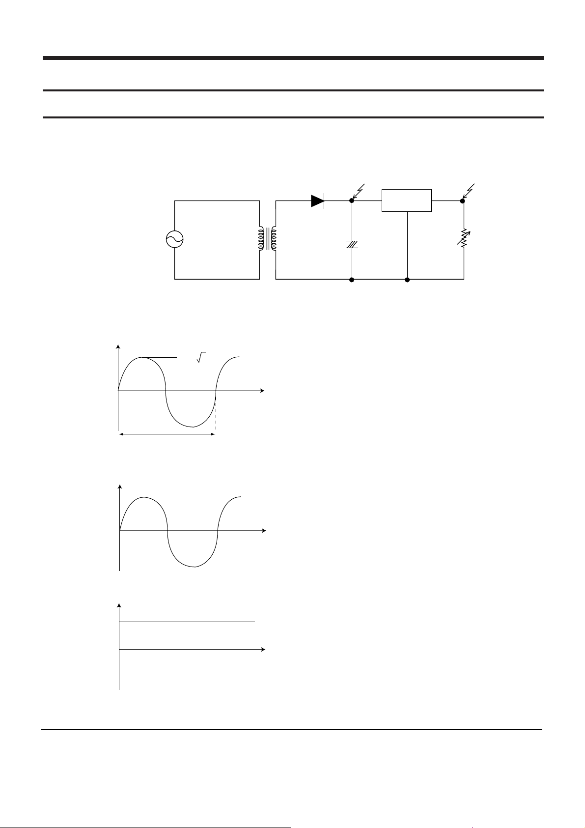
Fig. 7-1 Linear Power Supply
Input : Common power to transformer(Vp)
Fig. 7-2
The output Vs of transformer is determined by the ratio of
1st Np and 2st Ns.
Vs = (Ns/Np) x Vp
Fig. 7-3
Vout is output (DC) by diode and
condensor.
Fig. 7-4
7. Circuit Descriptions
7-1 SMPS
Vreg
Vout
+
–
+
+
–
Vs
(Ns)
Vp
(Np)
Regulator
Common power
(Ex.220V60Hz)
Vs
t
0
Vs
t
0
Vout
t
0
3 Waveform/Description
20µs
220 2V
Circuit Descriptions
7-2
Samsung Electronics
3 Advantages and disadvantages of linear power supply
a. Advantages :
Little noise because the output waveform of transformer is
sine wave.
b. Disadvantages :
» Additional margin is required because Vs is changed
(depending on power source). (The regulator loss is
caused by margin design).
» Greater core size and condensor capacity are needed,
because the transformer works on a single power
frequency.
Fig. 7-5
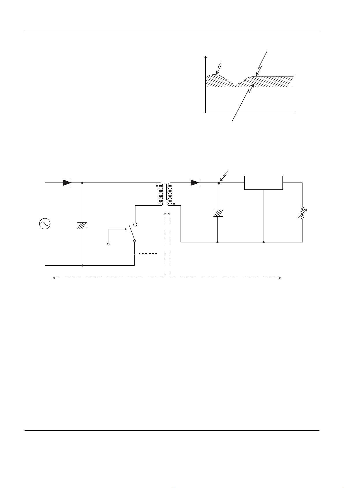
7-1-1(B) SMPS(PULSE WIDTH MODULATION METHOD)
Fig. 7-6 SMPS
3 Terms
- 1st : Common power input to 1st winding.
- 2nd : Circuit followings output winding of transformer.
- f(Frequency) : Switching frequency(T : Switching cycle)
- Duty : (Ton/T) x 100
V
Vreg
Vout
0 t
Change by common power
Regulator loss
Transformer Vout
(Np)
(Vp)
Switch
Vs switch
I switch
Vin
ON/OFF Control
+
–
+
–
+
+
+
–
(Vs)
(Ns)
Regulator
Circuit Descriptions
Samsung Electronics 7-3
7-1-2 Circuit description(FLY-BACK PWM(Pulse Width Modulation) control)
7-1-2(a) AC power rectification/smoothing terminal
- PD01,PD02,PD03,PD04 : Convert AC power to DC(Wave rectification)
- PO03 : Smooth the voltage converted to DC(Refer to VIN of Fig. 7-7)
- PC01, PC02, PC10, PC11, PC12, PC13, PL01, PL02, PL03 : Noise removal at power input/output
- PVA1 : SMPS protection at power surge input
(PVA1 pattern open is to remove noise)
- PR10 : Rush current limit resistance at the moment of power cord insertion.
» Rush current = (AC input voltage x 1.414 - Diode drop voltage) / Pattern resistance + PL02,01
resistance + PC10 resistance + PR10) (AC230V based : approx. 26A)
» Without PR10, the bridge diode might be damaged as the rush current increases.
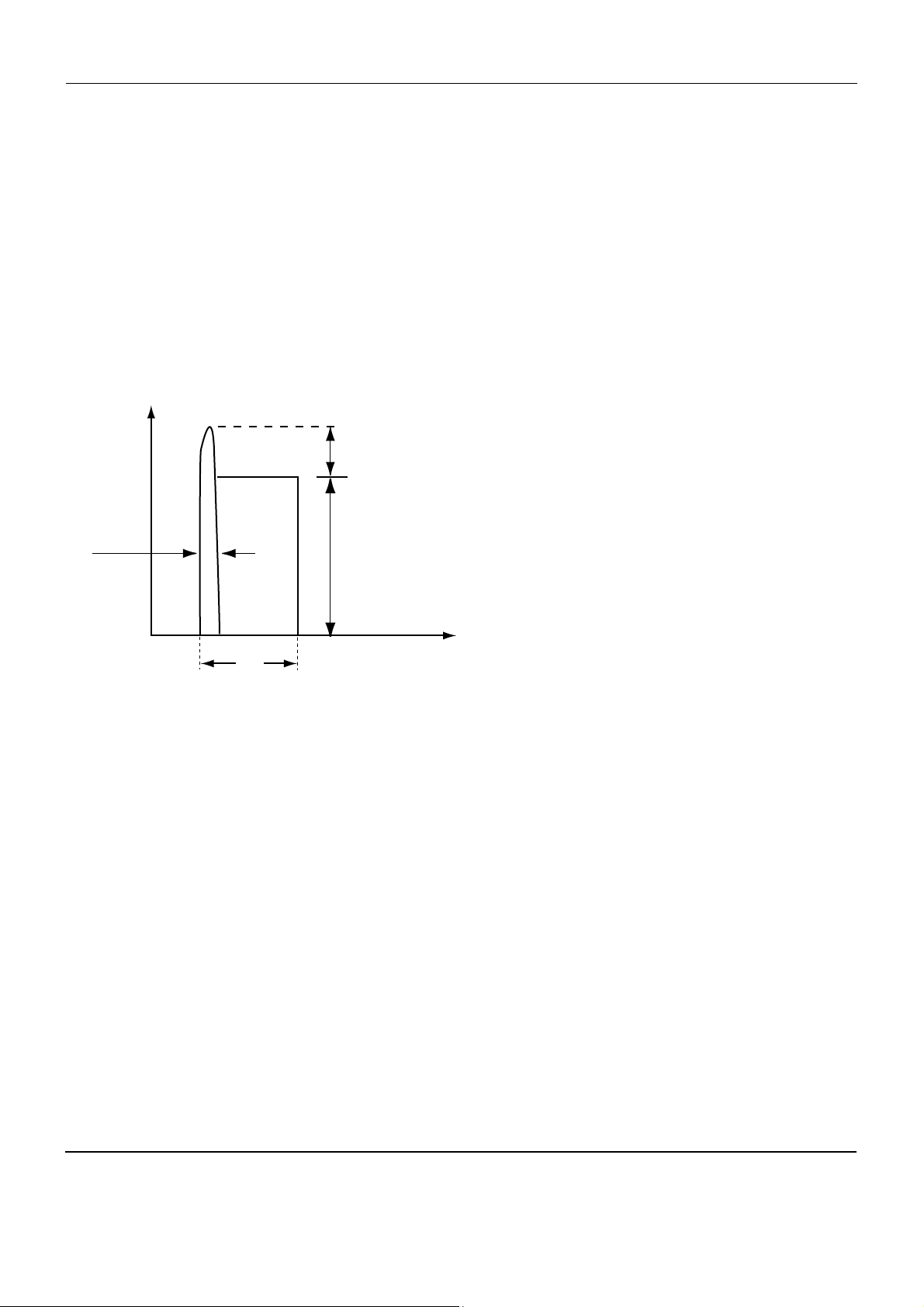
7-1-2(b) SNUBBER circuit : PR15, PR16, PC04, PD05, PD11, PR17
- Prevent residual high voltage at the terminals of
switch during switch off/Suppress noise.
High inverted power occurs at switch (PIC1) off,
because of the 1st winding of transformer:
(V=L1xdi/dt. LI : Leakage Induction)
A very high residual voltage exists on both
terminals of PIC1 because dt is a very short.
- SNUBBER circuit protects PIC1 from damage
through leakage voltage suppression by RC,
(Charges the leakage voltage to PD11 and PC04,
and discharges to PR15 and PR16).
- PC05, PL17 : For noise removal
Fig. 7-7
7-1-2(c) PIC1 Vcc circuit
- PR11, PR12, PR13, PR14 : PIC1 driving resistance (PIC1 works through driving resistance at power cord in)
- PIC1 Vcc : PR18, PD12, PC06
1) Use the output of transformer as Vcc, because the current starts to flow into transformer while PIC1 is active.
2) Rectify to PD12 and smooth to PC06.
3) Use the output of transformer as PIC1 Vcc : The loads are different before and after PIC1 driving.
(Vcc of PIC1 decreases below OFF voltage, using only the resistance due to load increase after PIC1 driving.)
0
Vswitch
dt
Toff
t
Inverted power
by leakage
inductance
Circuit Descriptions
7-4
Samsung Electronics
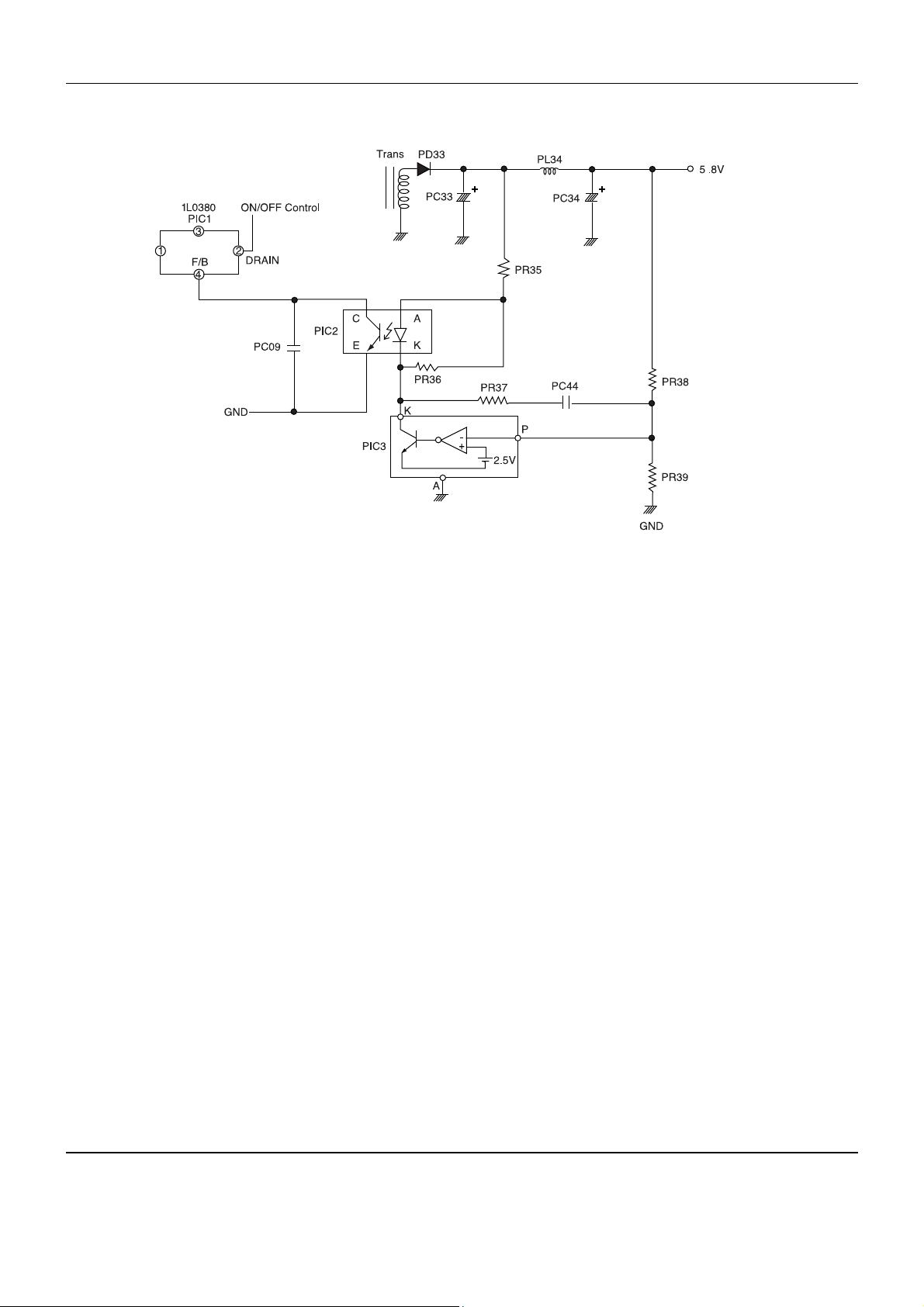
7-1-2(d) Feedback control circuit
Fig. 7-8
- F/B terminal of PIC1 determines output duty cycle.
- C-E(Collector-Emitter) of PIC2 and F/B potential of PIC1 are same.
3 Operation descriptions
a. Internal OP-Amp ‘+’ base potential of PIC3 is 2.5V and external “-” input potential is connected with PR38
and PR39 to maintain Vout of 5.8V. (Vout = ((PR36 x PR39) / PR39) x 2.5V)
b. If load of 5.8 V terminal increases(or AC input voltage decreases) and Vout decreases below 5.8V, then :
PIC3 ‘P’ potential down below 2.5V --> PIC3 A-K of base current down --> PIC3 of A-K current down -->
PIC2 Diode current down --> PIC2 C-E current down --> PIC2 C-E voltage up --> PIC1 F/B voltage up -->
Out Duty up --> Transformer 1st current up --> Transformer 1st power up --> Vout up --> Maintain
Vout 5.8V
c. If load of 5.8 V terminal decreases(or AC input voltage rises) and Vout rises above 5.8V, then :
Reverse sequence of the above description Æ Duty down Æ Vout down Æ Maintain 5.8V
(i.e., the feedback to maintains 5.8V).
- PR35, PR36 : Reduce 5.8V overshoot
- PR37, PC44 : Prevent PIC3 oscillation(for phase correction)
- PC09 : Adjust feedback response rate
1st
2nd
Circuit Descriptions
Samsung Electronics 7-5
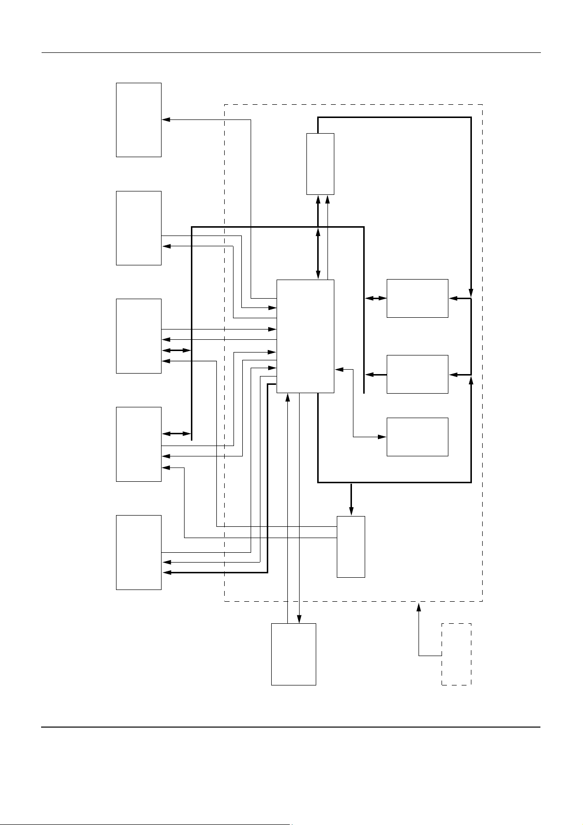
7-1-3 Internal block diagram
7-1-3(a). Internal block diagram of SMPS circuit
Fig. 7-9
7-1-3(b). PIC1(1L0380) internal block diagram
Fig. 7-10
Voltage
Ref.
UVLO
#3 Vcc
#2
Drain
#1
Source
GND
Sense
CCoonnttrrooll IICC
SS ee nnss ee
FF EE TT
S
Q
R
S
Q
R
osc.
Vck
32V
#4
Feedback
LEB
Reset
7.5V
5v
Reset
Thermal
Proction
OVP
2uA
6.3V
Sync.
2.5R
Voffset
Rsense
R
+
_
+
_
1mA
Noise
removal
(SNUBBER)
Smoothing
circuit
Rectified circuit
Line filter
Power IN
(85~265V)
FLT driving
circuit
5V rectified
smoothing circuit
3.3V rectified
smoothing circuit
Converter
PWM control cir-
cuit (1L0380)
Voltage
detection
circuit
8V rectified
smoothing circuit
-8V rectified
smoothing circuit
5V rectified
voltage
circuit(x2)
3.3V rectified
voltage
circuit
Moter 8V 1
port
8V rectified
voltage
circuit
-8V rectified
voltage
circuit
O
U
T
P
U
T
7-6
Samsung Electronics
7-2-1 RIC1(TA1236F)
TA1236F is combined with TA1253FN, TC9240F and TC90A19F as bipolar IC developed for DVD SERVO system.
Main features include DVD waveform equalizing, CD waveform equalizing, focus error signal generation, 3-beam
tracking error signal generation, laser power control, etc. after receiving the pick-up output converted into I/V.
7-2-1(a) Basic potentiometer
TA1236F uses a single power method and each circuit is based on VREF of 2.1V. Note :
symmetrical about GND for VREF because VREF(pin20) terminal is needed for IC, which uses the peripheral VREF
and 2VREF output(pin18).
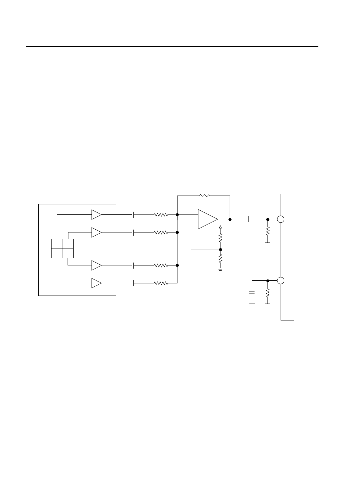
7-2-1(b) RF signal
Fig. 7-11 shows the flow of signal generated by the pick-up.
A, B, C, D signals detected from pick-up are converted in to RF signal(A+B+C+D) via RF summing AMP.
RF signal is inputted to RFN(pin55) among input terminals and RFP(pin54) is used for AC ground.
Fig. 7-11
Fig. 7-12 shows the waveform-equalizing block diagram for the RF signal.
It outputs to EQout(pin 46) terminal by initially changing switching AMP gain of DVD and CD, and then
adjusting the level in VCA. It controls VCA gain by means of RF gain(pin 48) and interfaces with PWM signal,
(output from RFGC terminal of TC9420F, via low-pass filter to constitute a loop for adjustment of constant
amplitude). The gain in EQout is 1.0 for DVD and 1.67 for CD.
EQout terminal is connected with EQin(pin 45) externally, and inputs into DVD EQ and CD EQ(Waveform
equalizing circuit).
55
54
PICK-UP
PD
D A
C B
I-V AMP
RC12
104
RR20
1K
RC10
104
RR19
1K
+
–
RC15
104
RR24
1K
RC14
104
RR22
1K
RR18
1.2K
RIC3 OPA650
SUMMING AMP
2
3
6
RC11
104
RR23
10K
RR50
5.6K
RR51
5.6K
RC22
104
RR33
10K
Vref
RIC1
TA1236
RFN
Vref
RFP
+5A
7-2 RF circuit description

Circuit Descriptions
Samsung Electronics 7-7
Fig. 7-12
The control parameters of DVD EQ and CD EQ are as follows.
1) DVD EQ control parameter
- DVDEQ(pin 43) : Changes the gain of peak frequency with EQ frequency characteristic. Convert PWM
signal, output from TC90A19F, into DC via low-pass filter.
- DVDTIME(pin 41) : Changes the peak frequency with EQ frequency characteristic. Convert PWM signal,
output from TC90A19F, into DC via low-pass filter.
- S/Dse1(pin 64) : Changes the peak frequency (like DVD TIME) as 2d control. ( Switched according to
regeneration speed ratio of single/double layer).
- MCK(pin 15) : Input the base clock and link the peak frequency with it. The amplitude of MCK might be
small (500mVp-p).
- DVDGD(pin 25) : Changes the group delay characteristics with EQ frequency characteristic.
2) CD EQ control parameter
- CD EQ(pin 40) : Changes the gain of peak frequency with EQ frequency characteristic. The constant DC
is supplied to a resistive voltage divider.
- CD TIME(pin 42) : Changes the peak frequency with EQ frequency characteristic. The constant DC is
supplied to a resistive voltage divider.
- S/Qse1(pin 44) : Changes the peak frequency (such as CD TIME) as 2d control. (Switched according to
play linear velocity ratio of quadruple/single rate. Set to ‘0’ because only one rate is
vaild in this system).
DVDsel RFgain EQout EQin
CDEQCD
TIME SQsel
RFN
RFP
47 48 46 45 40 42 44
55
54
64 41 43 15
34
25
39
VCA
ATT
CD EQ
DVD EQ
RIC1
TA1236F
GEN.
T/CON
SDsel DVD
TIME
DVDEQMCK
DVD G/D
DVD EQ OUT
CD EQ OUT
CD and DVD signals are equalized according to the above control parameters ,and then output to CD
EQ OUT (pin39) and DVD EQ OUT (pin34). Then, CD signal is transferred to TC9420F (pin 38), DVD
signal is sent to TC90A19F(pin 50) and detected.

7-8
Samsung Electronics
7-3 System control
7-3-1 Outline
The main micom peripheral circuit is composed of 16bit Micom(MIC1,TMP93CS41), 2M PROM (MIC2,AM27C020
for Microcode and data save, 1M SRAM(MIC3, KM681000) for data read/write on running, 512 byte EEPROM
(MIC5, IS24C02)for permanent storage of data needed at power off, MIC4(74AC573) to latch only address in the
bus where address and data are mixed, address decoder (MIC6, 74HC00) for selection of external device chip and
20MHz clock oscillator for micom operation. The micom(MIC1, TMP93CS41) mounted in main board analizes the
key commands of front panel or instructions of remote control through communication with micom(FIC1,
LC86P6232) of front and controls the devices on board to execute the corresponding commands after initializing the
devices connected with micom on board at power on.
Circuit Descriptions
Samsung Electronics 7-9
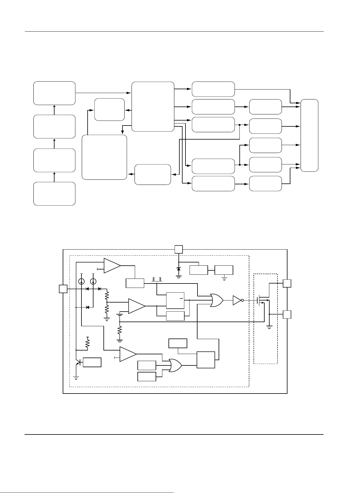
7-3-2 Block diagram
Fig.7-13
AIC1,2,3
D/A CONVERTER
PCM1720,1723
AIC1
VIDEO ENCODER
SAA7128
MIC4
74AC573
LOW ADDRESS
HIGH ADDRESS
DATA BUS
MIC1
MAIN MICOM
TMP93CS41F
FIC1
FRONT
MICOM
LC86P6232
MIC6
ADDRESS
DECODER
MICOM
BLOCK
MIC5
EPROM
IS24C02
MIC2
EPROM
AM27C020
MIC3
SRAM
KM681000
BIC1
A/V DECORDER
ZiVAD6-L
DIC1
DVD PROCESSOR
TC90A19F
SIC7
CD PROCESSOR
TC9420F
 Loading...