

Samsung DVD-808 Reference Information

Samsung Electronics 2-1
2. Reference Information
2-1 Semiconductor Base Diagram
Fig. 2-1
RQ1
SS9012
S9012
G-634
E B C
D G S
K184
Y 6A
SQ1
K184

2-2 Samsung Electronics
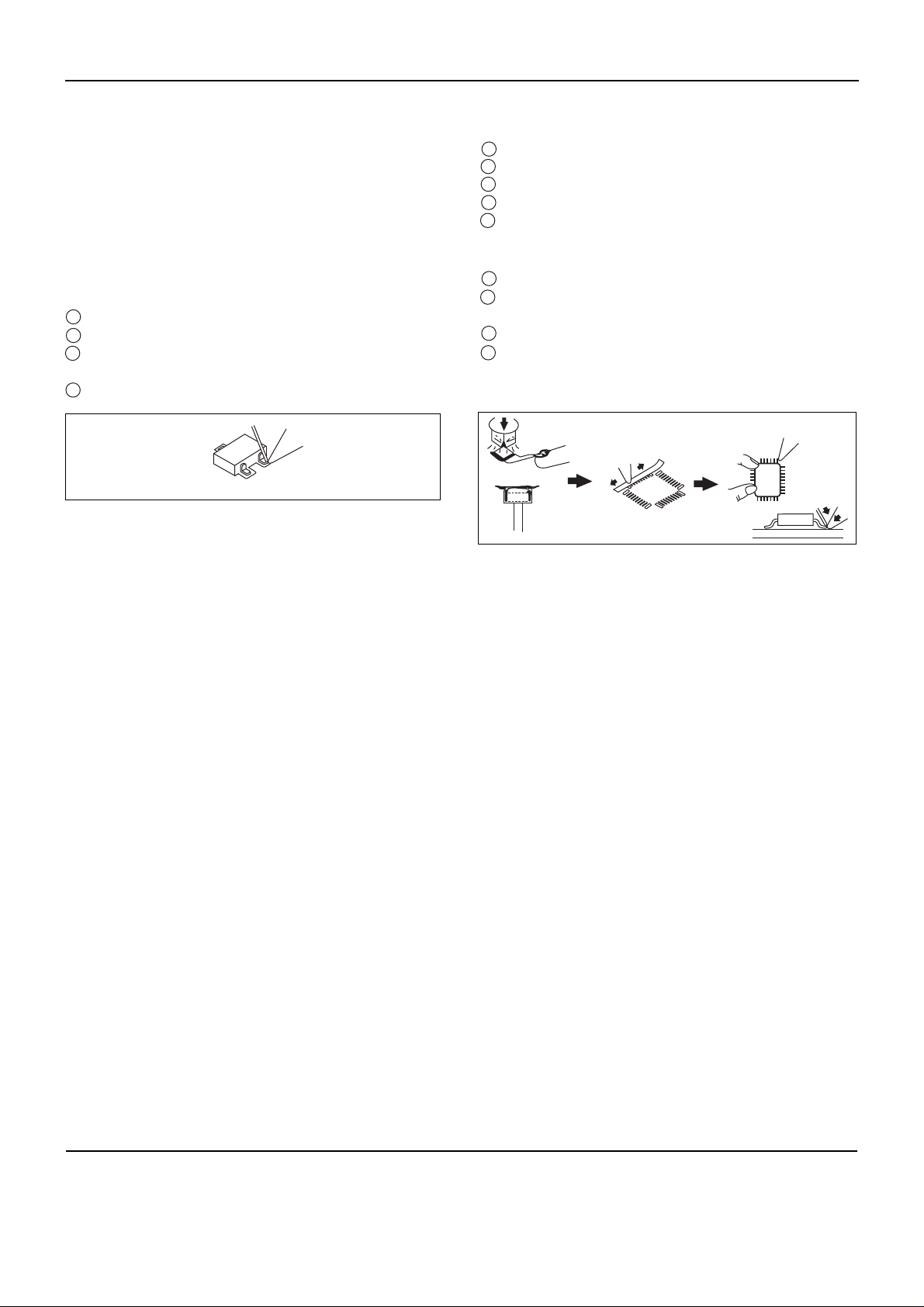
2-2 Chip Replacement
1) Do not touch the part body directly with the soldering iron. ICs, especially TSOP, are easily damaged by heat.
2) Use care regarding soldering iron tip and avoid
repidly heating parts. Some parts can be damaged
by sudden heating. Preheat the part at about
100°… for several minutes before installing it.
3) Use soldering tip temperature of about 240°… or
larger parts, use a slightly higher temperature
(about 280°…).
4) The thin(0.3mm)solder for miniature parts does
not contain adequate flux. Supplementary flux is
thus needed in most cases.
5) Use care not to damage the circuit pattern, especially when removing.
6) Because of the many pins, cleanliness of the pattern is extremely important after removing the IC.
7) Use care to avoid solder bridges. Remove any that
occurs.
8) Position the part carefully. They will also affect the
soldering operation. Be very precise in positioning
the IC. Soldering opposite pins first holds the IC in
place and makes soldering the other pins easier.
9) Do not reuse removed parts.
10) Check for solder joints, especially miniature parts
with small lead.
11) A defective trimming resistor cannot be adjusted
externally. Replace with an ordjnary variable resistor.
12) It is important to inspect the work with a magnifier.
Check after installing (cold solder joints, etc.).
2-2-1 Precaution for the chip Replacement
The tools for the chip replacement are as follows:
1) Thin tip type soldering iron
2) Small flat-blade tip-type soldering iron
3) Special desoldering tip iron
4) Airblower unit
5) Flat Package Pick-up
6) Flux can be cleaned by water
7) 0.3mm thin solder can be cleaned by water
8) Desoldering wire
9) Tweezers
2-2-2 Tools for the Chip Replacement
2-2-3 Chip Resistors and Chip Capacitors
-- Kind of the Part
The kind of chip resistors and chip capacitors as follows:d
1) Think Film Chip Resistors
2) Carbon Film Chip Resistors
3) Metal Film Chip Resistors
4) Chip Ceramic Capacitors
5) Chip Trimming Resistors
-- Removing the Part
1) Using two soldering irons:
Use thin tip soldering irons.
Use soldering tip temperature of about 280°….
Simultaneously heat both ends of the part.
While heating, grasp the part with the tips of the
soldering irons and remove it.
Use desoldering wire to completely remove the old
solder from the part location of the board.
A clean pattern for installing the new part is very
important.
Fig 2-2
-- Installing the Part
1) Use desoldering wire to remove the previous solder.
2) Clean the location.
3) Apply flux.
4) Position the IC and solder two pins at opposite sides.
5) Use a sharp tipped soldering iron and carefully
solder each Pin.(After gaining experience, a thicker
tip can be used for better work efficiency.)
6) Remove any solder bridges with desoldering wire.
7) Inspect the work with a magnifier.
1
2
3
4
5
6
Precautions
Samsung Electronics 2-3
-- Kind of the Part
The kind of the part is as follows:
1) Chip VRs.
2) Chip Trimmer Capacitors
3) Diode
4) Transistors
-- Removing the Part
1) Using two soldering irons:
Use small flat-blade tips.
Heat the leads of the part simultaneously.
When the solder melts, grasp and remove the part
with the soldering iron tips.
Remove the old solder with desoldering wire.
2-2-4 Diodes and Tr.
-- The kind of the Chip ICs
The kind of the chip ICs are as follows:
1) SOP(Small Outline Package)IC
2) SSOP(Shrink Small Outline Package)IC
3) VSOP(Very Small Outline Package)IC
4) QFP(Quad Flat Package)IC
5) VQFP(Very Quad Flat Package)IC
6) PLCC(Plastic Leaded Chip Carrier)IC
7) TSOP(Thin Small Outline Package)IC
2-2-5 Chip ICs
-- Removing the Part
1) Using special desoldering iron:
Selet the tip according to the size and shape of the IC.
“Tin” the tip with a small amount of the IC leads.
Set the tip squarely over the IC leads.
When the solder melts, carefully twist the iron.
Raise and remove the IC.
2) Using shaped airblower unit:
Select the correct nozzle.
Select the temperature and airblow(suggested:
temperature:7, airblow:4)
Engage the IC removing tool.
Use the airblow to preheat the IC for about 5
seconds, then heat with the nozzle until the IC
remover lifts the part from the board.
IC
Fig 2-4
-- Installing the Part
1) Use desoldering wire to remove the previous solder.
2) Clean the location.
3) Apply flux.
4) Position the IC and solder two pins at opposite sides.
5) Use a sharp tipped soldering iron and carefully sol
der each Pin.(After gaining experience, a thicker tip
can be used for better work efficiency.)
6) Remove any solder bridges with desoldering wire.
7) Inspect the work with a magnifier.
Fig 2-3
-- Installing the Part
1) Clean the area where the new part is to be mounted.
2) Apply flux.
3) Set part correctly into position, prevent it from shifting.
4) Use sharp soldering iron tip. Bring close to the
part contact without actually touching it. Melt thin
solder between the tip and part si that it flows into
the part contact.
1
234
123
45123
4

Precautions
2-4 Samsung Electronics
MEMO

Samsung Electronics 6-1
6. IC Descriptions
List
6-1
6-2
6-3
6-4
6-5
6-6
6-7
6-8
15-1-3 Data Processor
15-1-1 Micom
MIC1
MIC2
TMP93CS41
MAIN MICOM
4Megabit(512K 8-bit) CMOS EPROM
128K 8 bit CMOS SRAM
RF IC
DPD IC
3-PHASE MOTOR DRIVER
SERVO & CD DATA PROCESSOR
DVD DATA PROCESSOR
512K 8 bit CMOS DRAM
AUDIO/VIDEO DECODER
EPROM
CMOS DRAM
DIGIT AL-TO ANALOG CONVERTER
DIGIT AL-TO ANALOG CONVERTER
DIGITAL VIDEO ENCODER
FRONT MICOM
ECHO SOUND PROCESSOR
Am27C040
KM681000
TA1236F
TA1253F
BA6840
TC9420F
TC90A19F
KM48C512
ZiVA D6-L
AM27C4096
KM416C254DJ
AK4324
PCM1720
PCM1723
SAA7128
LC86P6232
ES56033
MIC3
RIC1
RIC2
SIC5
SIC7
DIC1
DIC2
BIC1
BIC2
AIC1
AIC2
AIC3
VIC1
FIC1
KIC1
15-1-2 Servo
15-1-4 A/V Decoder
15-1-5 Audio
15-1-6 Video
15-2 Front Board
15-4 Karaoke Board
6-9
6-10
6-11
6-12
BIC3,BIC4,BIC5,BIC6,BIC7
6-13
6-14
6-15
DIGITAL-TO ANALOG CONVERTER WITH PLL
6-16
6-17
6-18
SCHEMATIC
LOCATION DEVICE FUNCTION
6-2 Samsung Electronics
6-1 MAIN MICOM (MIC1 : TMP93CS41)
PAO~PA6
PA7(SCOUT)
P50 to P57
(ANO to AN7)
AVCC
AVSS
VREFH
VREFL
(TXD0)P90
(RXD0)P91
(SCLK0/CTS0)P92
(TXD1)P93
(RXD1)P94
(SCLK1)P95
(PG 00)P60
(PG 01)P61
(PG 02)P62
(PG 03)P63
(PG 10)P64
(PG 11)P65
(PG 12)P66
(PG 13)P67
(T10)P70
(T01)P71
(T02)P72
(T03)P73
(INT4/T14)P80
(INT5/T15)P81
(T04)P82
(T05)P83
(INT6/T16)P84
(INT7/T17)P85
(T06)P86
(INTO)P87
VCC[3]
VSS[3]
X1
X2
CLK
XT1
XT2
AM8/16
EA
RESET
ALE
TEST2,1
NMI
WDTOUT
P00 to P07
(AD0 to AC7)
P10 to P17
(AD8 to AD15/A8 toA15
P20 to P27
(A0 to A7/A16 to A23)
P30(RD)
P31(WR)
P32(HWR)
P33(WAIT)
P34(BUSRQ)
P35(BUSAK)
P36(R/W)
P37(RAS)
P40(CS0/CAS0)
P41(CS1/CAS1)
P42(CX2/CAS2)
cPORT A
High
Frequency
OSC
Low
Frequency
OSC
INTERRUPT
CONTROLLER
WATCH-DOG
TIMER
PORT 0
PORT 2
PORT 3
CS/WAIT
CONTROLLER
(3-BLOCK)
PORT 1
10-BIT 8CH
A/D
CONVERTER
SERIAL I/O
(CH,0)
SERIAL I/O
(CH,1)
PATTERN
GENERATOR
(CH,0)
PATTERN
GENERATOR
(CH,1)
16BIT TIMER
(TIMER 4)
16BIT TIMER
(TIMER 5)
8BIT TIMER
(TIMER 0)
8BIT TIMER
(TIMER 1)
8BIT PWM
(TIMER 2)
8BIT PWM
(TIMER 3)
900L-CPU
2KB RAM
XWA
XBC
ADE
XHL
XIX
XIY
XIZ
XSP
W
B
D
H
IX
IY
IZ
SP
A
C
E
L
32bit
FSR
P C
BLOCK DIAGRAM

IC Descriptions
6-3Samsung Electronics
PIN ASSIGNMENT
IC Descriptions
6-4 Samsung Electronics
VSS
VCC
A16
A17
A18
A19
A20
A21
A22
A23
/RD
/WR
ML0/DIF0
WAIT
/BUSRQ
/BUSAK
ED_K
ED_T
/CS0
/CS1
/CS2
DVD_SEL
OPEN
CLOSE
S/D_SEL
SDA
SCL
BASS
SLEDGS
WDTO
V
SS
V
CC
A16
A17
A18
A19
A20
A21
A22
A23
P30
P31
P32
P33
P34
P35
P36
P37
P40
P41
P42
P60
P61
P62
P63
P64
P65
P66
P67
61
62
63
64
65
66
67
68
69
70
71
72
73
74
75
76
77
78
79
80
81
82
83
84
85
86
87
88
89
90
I/O
O
O
O
O
O
O
O
O
O
O
O
I
I
O
O
O
O
O
O
O
O
O
O
O
O
O
O
GND(0V)
+5V
Address Bus 16
Address Bus 17
Address Bus 18
Address Bus 20
Address Bus 21
Address Bus 22
Address Bus 23
Strobe for Reading External Momory
Strobe for Writing Data AD0 to AD7
Audio DAC Data Latch 0
/AKM4324 Control(“L”=16/24bit, “H”=20bit)
Address Bus 19
Request CPU Bus Wait
Bus Request
Bus Acknowledge
EEPROM Trans. Clock(I2S)
EEPROM Trans. Data(I2S)
Chip Select 0
Chip Select 1
Chip Select 2
DVD/CD Mode Control(DVD=”Low”)
Door Open Motor Control
Door Close Motor Control
Single/Dual Disc Select(Single=”Low”)
Video Encoder Trans. Data(l
2
C)
Video Encoder Trans. Clock(l
2
C)
Bass Redirection Control(“L”=SW On, “H”=SW Off)
Sled Gain Select
FUNCTION
PIN I/O NAME
FUNCTION
PIN I/O NAME
VSS
FEI
SPFG
/SECAM
/PAL
/NTSC
OP-SW
CL-SW
VREFH
V
SS
P50
P51
P52
P53
P54
P55
P56
P57
VREFH
91
92
93
94
95
96
97
98
99
100
I
I
I
I
I
I
I
I
I
GND
Focus Error Input
Spindle FG Input
SECAM=”H”
PAL =”H”
NTSC=”H”
Door Open SW
Door Close SW
Reference Voltage Input to A/DC(¡ H¡–)
PIN ASSIGNMENT
6-5Samsung Electronics
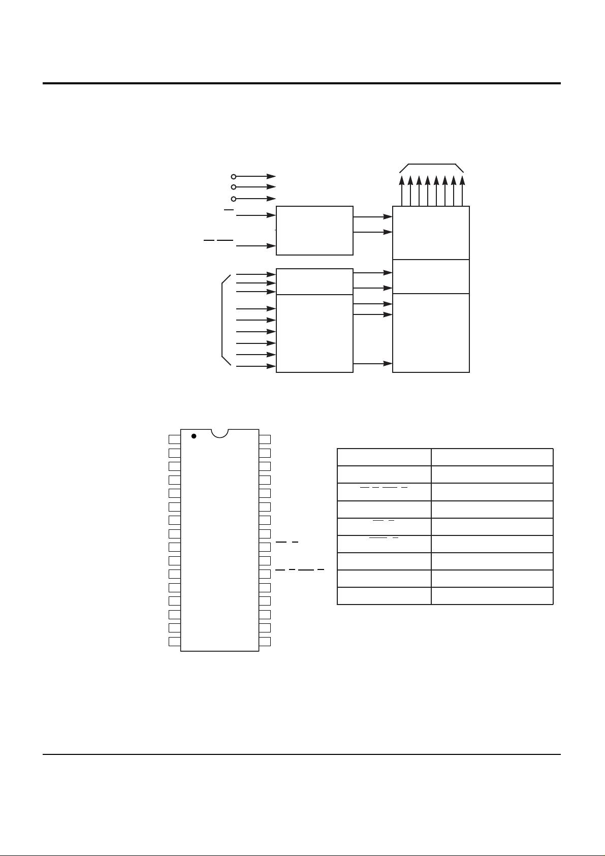
6-2 4Megabit (512K, 144 x 8-bit) CMOS EPROM (MIC2 ; Am27C040)
NAME
A0-A17
CE (E)
DQ0-DQ7
OE (G)
PGM (P)
Vcc
Vpp
Vss
1
2
3
4
5
6
7
8
9
10
11
12
13
14
15
16
Vpp
A16
A15
A12
A7
A6
A5
A4
A3
A2
A1
A0
DQ0
DQ1
DQ2
Vss
Vcc
PGM (P)
A17
A14
A13
A8
A9
A11
OE (G)
A10
CE (E)
DQ7
DQ6
DQ4
DQ4
DQ3
32
31
30
29
28
27
26
25
24
23
22
21
20
19
18
17
TOP VIEW
Output Enable
Chip Enable and
Prog Logic
Output Buffers
Y
Gating
2,097,152-Bit
Cell Matrix
Y
Decoder
A0-A17
Address
Inputs
OE
.
.
.
.
.
.
.
X
Decoder
Data Outputs
DQ0-DQ7
CE
Vpp
Vcc
Vss
CE/PCM
BLOCK DIAGRAM
FUNCTION
Address Inputs
Chip Enable Input
Data Input/Outputs
Output Enable Input
Program Enable Input
Vcc Syply Voltage
Program Voltage Input
Ground
PIN ASSIGNMENT
CE/PGM
8
4,194,304-Bit
CE (E)/PGM (P)
A18
18
CE (E)/PGM (P)
Chip Enable/Program Enable Input
6-6 Samsung Electronics
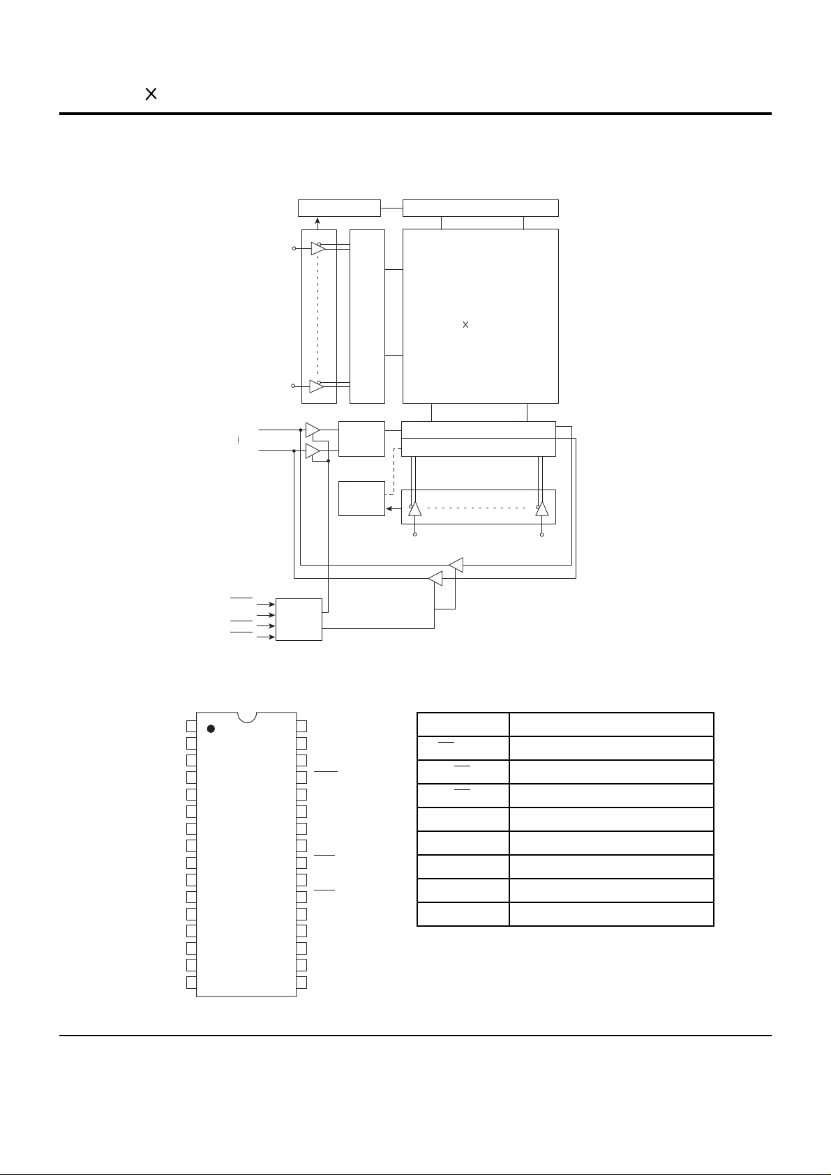
6-3 128K 8 bit CMOS SRAM (MIC3 ; KM681000B)
BLOCK DIAGRAM
Clk gen
Row
select
Data
cont
I/O
1
I/O8
CS1
CS2
WE
OE
I/O Circuit
Column select
A0 A1 A2 A3 A8 A9 A10 A11
Data
cont
Control
logic
Precharge circuit
Memory array
512 rows
256 8 columns
A4
A5
A6
A7
A12
A13
A14
A15
A16
1
2
3
4
5
6
7
8
9
10
11
12
13
14
15
16
17
18
19
20
21
22
23
24
25
26
27
28
29
30
31
32
32-DIP
32-SOP
N.C
A16
A14
A12
A7
A6
A5
A4
A3
A2
A1
A0
I/O1
I/O2
I/O3
VSS
VCC
A15
CS2
WE
A13
A8
A9
A11
OE
A10
CS1
I/O7
I/O8
I/O6
I/O5
I/O4
TOP VIEW PIN ASSIGNMENT
NAME
CS
1, CS2
FUNCTION
Chip Select Inputs
OE
Output Enable Input
WE
Write Enable Input
A0 ~ A16
Address Inputs
I/O1 ~ I/O8
Data Inputs/Outputs
Vcc
Power
Vss
Ground
N.C
No Connection

6-7Samsung Electronics
6-4 RF IC (RIC1 ; TA1236F)
BLOCK DIAGRAM
 Loading...