

Page 1
Circuit Description
Samsung Electronics 13-1
13. Circuit Description
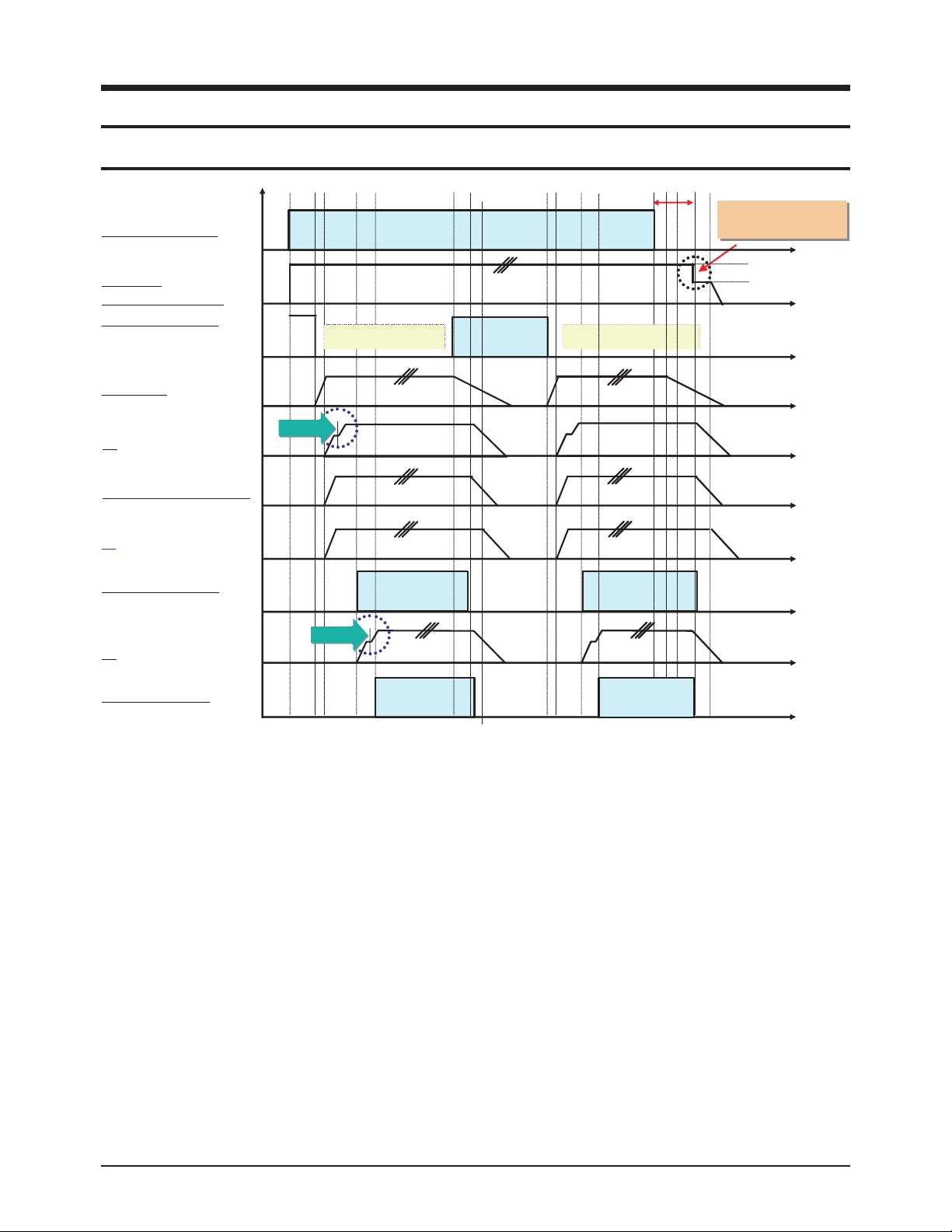
13-1 Power ON/OFF Signal Timing Sequence
µ
µ
1. When connecting the AC power cord, Stand-By 5V from the Main SMPS is supplied to the Main Board (Pin 3 of CN1002 of Main
Board).
2. When pressing the Power button on the remote control or on the main body, PS_ON (Pin 5 of CN1002 of Main Board)
changes from High to Low.
3. If the PS_ON signal changes to Low, the Main SMPS supplies power to the Main Board and Logic Board, and Va and Vg power
is supplied to the DC-DC SMPS.
4. If the VS_ON signal from the Logic Board changes from Low to High, the Main SMPS supplies VS power to the X and Y Drive
Board through the DC-DC SMPS, and the screen displays a picture on it.
W
OP C
A
(
E
B
,y
-
dnatS
itpO
o
POP(
A( NO_SP
txE SP morf
meR
o
et
tuptuo CFP
U
PTUO CD
aV
T
FFO/NO R
u
n
S
st
uo
)
pt
w
oL evitc
)
lanre
ellortnoc
)FF
O/NO r
cV
a
cV
a
WOP CA
NO rellortnoC etomeR
NO rellortnoC etomeR
07
.ceS m
.ceS m 07
ts ybdnatS
NO RE
NO
REWOP CA
FFO
FFO
oC etomeR
n
NO rellort
NO rellortnoC etomeR
rofµ
rofµ
V 5
V 5
V
4.3
V 4.3
ffo-nrut pe
o-nrut pets ybdnatS
ff
teser rossecorp-
teser rossecorp-
STUPTUO CD
STUPTUO
g
V
V
V
A( NO_S
s
YA
LPSID
lanretxE S/P morf
TUPTUO CD
O
N
t
V,pmaV,V21,V5.6A,V3.5D
)hgih evitc
V
sc
V
sc
FFO /
NO_S
V
NO_SV
D
NO YALPSID
NO YALPSI
O_SV
N
NO_S
V
NO YAL
PSID
NO YALPSID
Page 2
Circuit Description
13-2 Samsung Electronics
13-2 Partial Block Description
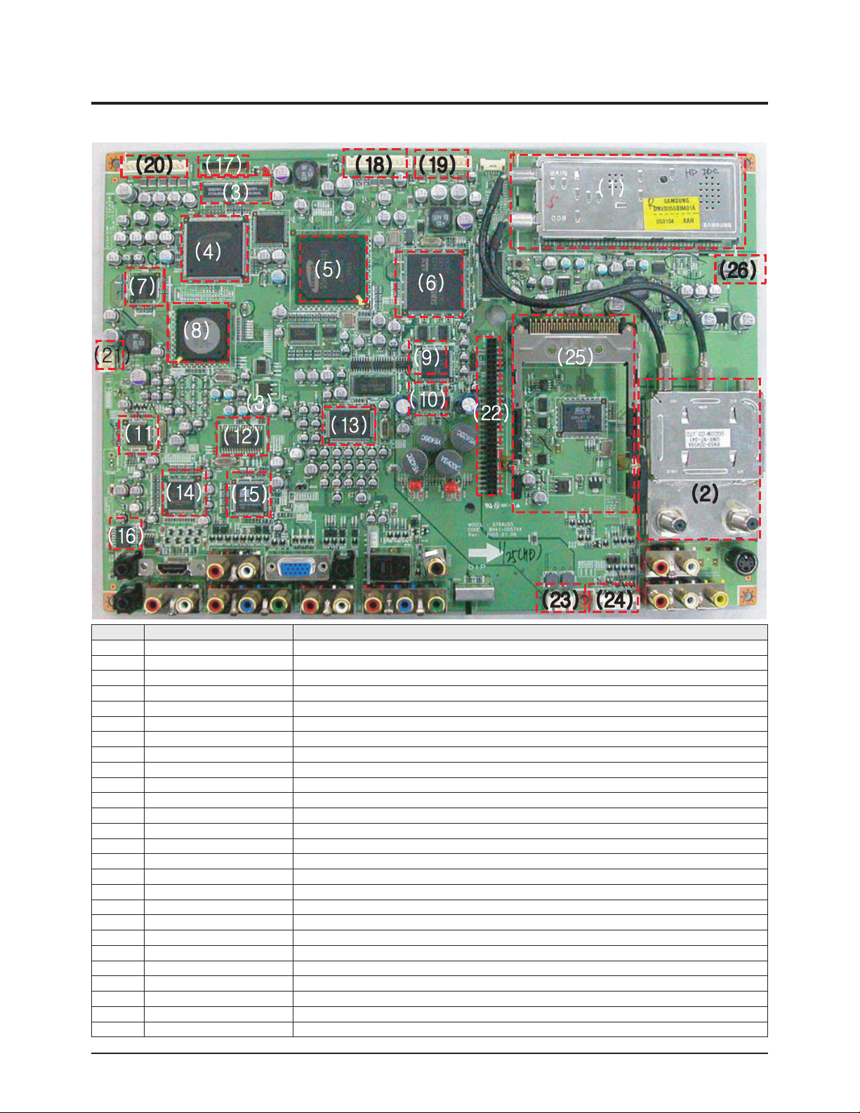
13-2-1 Main Board
No Loc. No. Description
(1) TU1002 (DNVS303EH261A) The Main Tuner.
(2) CN7001 (UMX-NT-043) The RF Splitter for selecting Antenna IN 1 or Antenna IN 2.
(3) IC9001,IC9003 (DTC34LM85AL) Converts the digital R, G, B signals from the main board into an LVDS signal and transmits the signal to the PDP Logic board.
(4) IC9002 (SDP43) The DNIe IC for visual quality improvement.
(5) IC7010 (S5H2010A01) MPEG Decoder IC
(6) IC6006 (S3C2800X01) CPU IC
(7) IC5003 (K4D263238E) SDRAM for STP22.
(8) IC5004 (STP22) A Scaler IC that generates the output resolution appropriate to the PDP panel and generates the PIP screen.
(9) IC2016 (NSP-6241A) Sound PWM IC
(10) IC2015 (TAS5122) Sound AMP IC
(11) IC3002 (3F866B) Generates various control signals required for operating the circuit. The software is downloaded through PC D-SUB Jack.
(12) IC3003 (P_PCFM_012) The Micom that inputs and outputs various control signals.
(13) IC2012 (MSP4440K) Sound Processing IC
(14) IC4005 (SIL9993) Converts the TMDS signal on the HDMI input into 8 bit digital R, G, B signals.
(15) IC4003 (MST9883) A/D converts the R, G, B input signal from 15 Pin PC video to 8 bit digital R, G, B signals.
(16) IC3006 (MAX232) RS-232 receiver IC
(17) JA9001 LVDS Logic Connector
(18) CN1002 SMPS Connector
(19) CN1001 SMPS Connector
(20) CN8002 SMPS-POD Connector
(21) CN1004 Function key board Connector
(22) 60P CONNECTOR for Debug (Option)
(23) CN2001 SPEAKER CONNECTOR
(24) CN1003 POWER&IR BOARD CONNECTOR
(25) CN8003 POD SLOT Connector
(26) CN8001 POD FAN Connector
Page 3
Circuit Description
Samsung Electronics 13-3
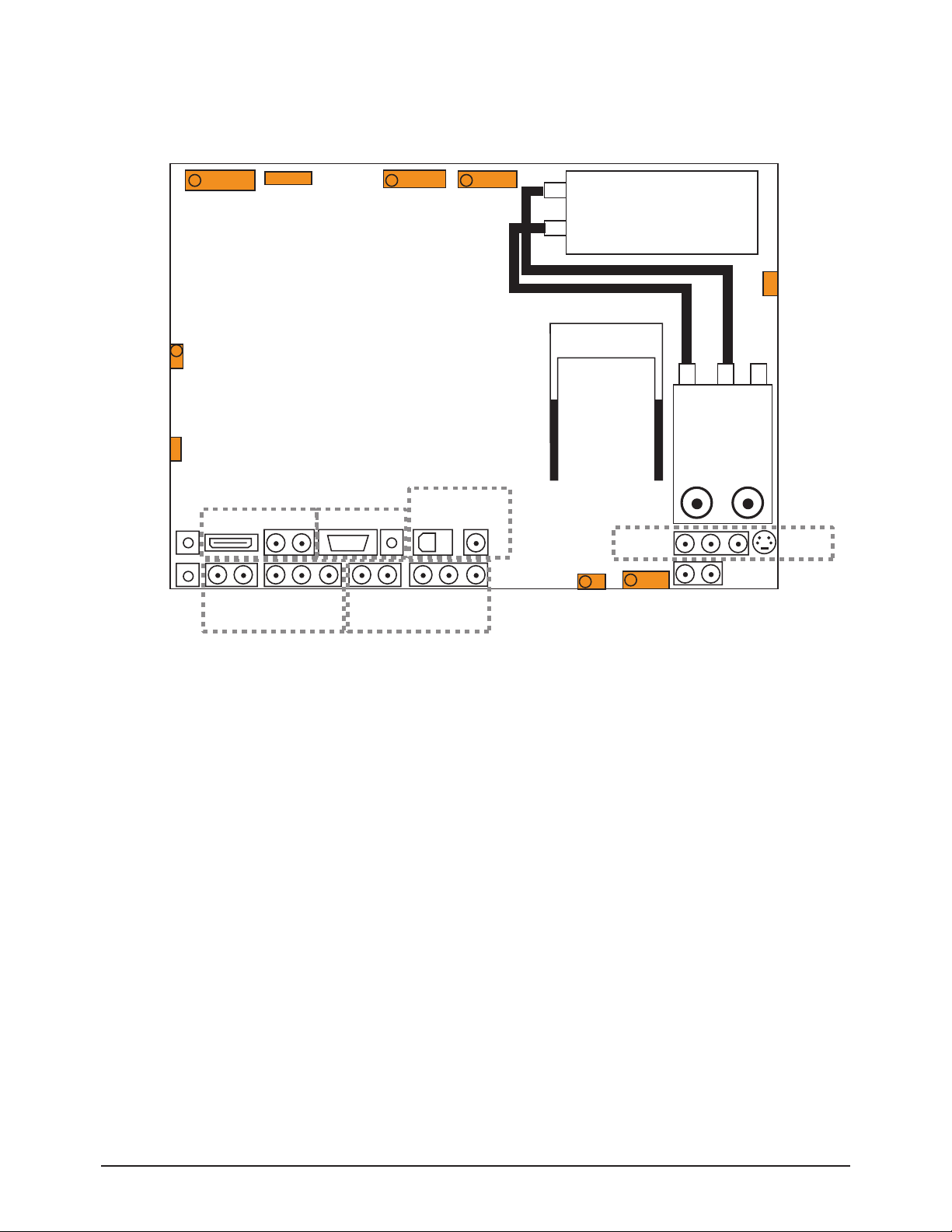
13-2-2 Connectors of Main board
Funcion
Connector
CN1004
Debug
Connector
TEST5001
SVC In
Anynet In
POD Power
CN8002
1 1
1. POD_SW
2.
3. GND
4. S_12V
5. GND
6. S_12V
7. GND
8. S_6.5V
9. GND
10. S_5V
11. GND
12. S_5V
1
1. KEY1
2. KEY2
3. GND
LVDS out
JA9001
HDMI DVI L/R PC In - Audio
Component 2
R-L-Pr-Pb-Y
Digital Power
CN1002
1.
2. THER_D
3. STD_5V
4. GND
5. PS_ON
6. D12V
7. GND
8. D3.3V
9. D3.3V
10. GND
11. D6V
Digital Out
Optical/Coaxial
Component 1
R-L-Pr-Pb-Y
Analog Power
CN1001
1
1. GND
2. VT(B33V)
3. GND
4. GND
5. 18V_A
6. 18V_A
7. GND
8. A12V
9. GND
10. +6V
MAIN
OOB
POD Slot
1
SPK.out
CN2001
1. R(-)
2. R(+)
3. L(-)
4. L(+)
ATSC Tuner
Video In
1
Power-IR
CN1003
1. GND
2. LED_RED
3. A5V
4. GND
5. KEY2
6. SDA
7. SCL
8. IR
FAN Conn.
CN8001
OOB MAIN SUB
Splitter
AirCable
S-Video
Monitor Out
Page 4
Circuit Description
13-4 Samsung Electronics
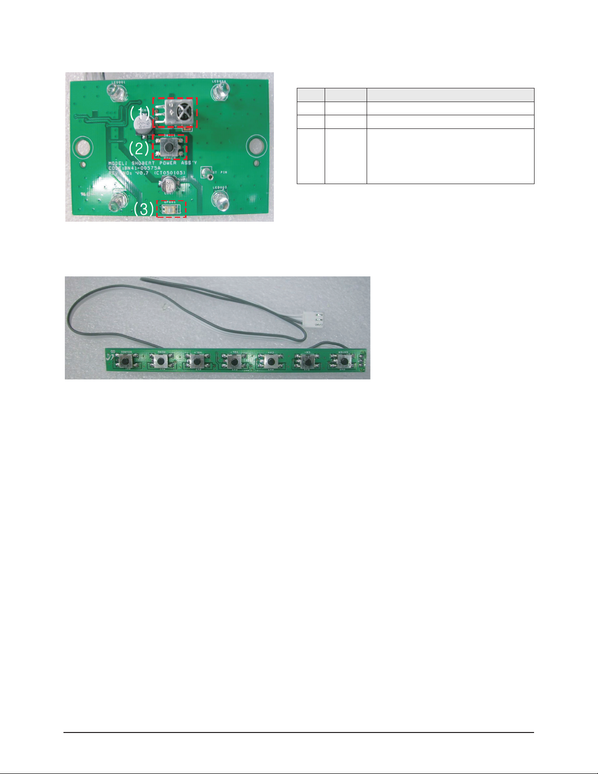
13-2-3 Power Button Board
13-2-4 Function Key Board
Function Key. Located on the side of the unit.
No Loc. No. Description
(1) RM01 Remote Control Sensor
(2) SW001 Power Button
(3) OP001
The Illumination sensor that senses the quantity of
light. It senses the illumination and automatically
adjusts the screen brightness according to the surrounding brightness when the Power Saving Mode
of the User menu is set to Auto.
Page 5
Circuit Description
Samsung Electronics 13-5
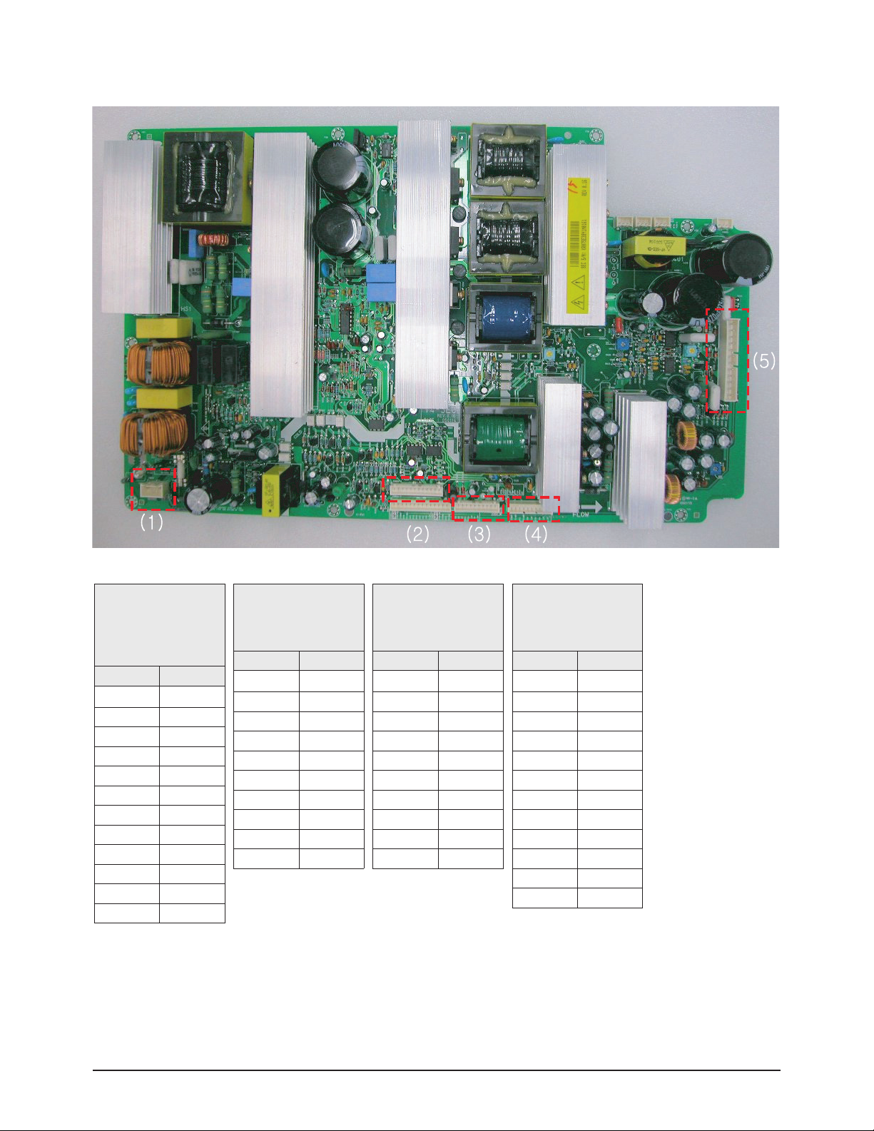
13-2-5 Main SMPS
(1) CN800: AC IN (90 ~ 264V)
※ CN811, CN806, CN807 and CN808 are not used.
(2)
CN804-1
MAIN SMPS
↔
CN1002(Main B'D)
Pin No Signal
1 ■
FAN-D
2 FAN-ON
3 STB5V
4 RTN
5 PS-ON
6 12V
7 RTN
8 RTN
9 VCA
10 VCS
11 RTN
12 5.3V
(3)
CN803(MAIN SMPS)
↔
CN1001(Main B'D)
Pin No Signal
1 ■
RTN
2 VT(33V)
3 RTN_AMP
4 RTN_AMP
5 18V_AMP
6 18V_AMP
7 RTN
8 12V
9 RTN
10 6V
(4)
CN810(Main SMPS)
↔
CN2013(Logic B'D)
Pin No Signal
1 ■
5.3V
2 5.3V
3 RTN
4 RTN
5 5.3V
6 RTN
7 PS-ON
8 N.C
9 VS-ON
10 STB 5V
(5)
CN809(Main SMPS)
↔
CN3(DC-DC SMPS)
Pin No Signal
1 ■
5.3V
2 Vg
3 RTN
4 RTN
5 RTN
6 RTN
7 RTN
8 Va
9 Va
10 N.C
11 Vs
12 Vs
Page 6
Circuit Description
13-6 Samsung Electronics
1. Outline (PDP 42inch/50inch SMPS)
Considering various related conditions, the switching regulator with good efficiency and allowing for its small size and light weight
was used as the power supply for PDP 42inch(Schubert)/50inch(Strauss), VS requiring high power consumption Asymmetrical Half
Bridge converter and flyback converter. To comply with the international harmonics standards and improve the power factor, active
PFC(Power Factor Correction) was used to rectify AC input into +400V DC output, which in turns used as input to the switching
regulator.
2. Input
The power supply shall be capable of supplying full rated output power over free voltage ranges that are rated 100 VAC - 240 VAC
RMS nominal. Operating voltage : 90 VAC - 264 VAC
The power supply must be able to start up under peak loading at 90V AC. The power supply shall automatically recover from AC
power loss. (Note that nominal voltages for test purposes are considered to be within +/- 1.0V of nominal).
STD_5V & Vpr2(3.3V) is a SELV standby voltage that is always present when AC mains voltage present.
3. Output
4. Over Voltage Protection
The over voltage sense circuitry and reference shall reside in package that are separate and distinct from the regulator control
circuitry and reference. No single point fault shall be able to cause a sustained over voltage condition on any or all outputs.
The supply shall provide latch-mode Over Voltage Protection as defined below.
5. Short Circuit and Over current Protection
An output short circuit is defined as output impedance of less than 300mohms. The power supply shall shutdown and latch off for
shorting VS DC rails to return. Shorts between main output rails and STD_5V shall not cause any damages to the power supply.
The power supply shall either shutdown and latch off until the short condition is removed, at which point the P/S shall recover. The
power supply shall be capable of withstanding a continuous short-circuit to the output without damage or over stress to the unit
(components, PCB traces,connectors,etc.) under the input conditions specified in Section 3 above. Current Protection as defined
below.
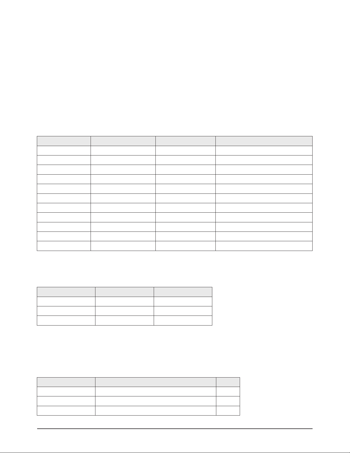
Output Name Output Voltage Output Current(Max.) Using in PDP Driving
VS +190V ~ 220V (210V) 2.0A Sustain Voltage of Drive Board
VA +60V ~ 80V (70V) 3.0A Address Voltage of Drive Board
D5.3V +5.3V 5.0A
A6.5V +6.5V 3.0A
FAN_9V +9V 0.2A
VG +15V 1.0A
D12V +12V 1.5A
A12V +5.3V 0.5A
18VAMP +18V 2.5A Amp Voltage of Audio Board
VT +33V 0.006A
STD_5V +5V 1.0A Standby for Remote Control
Parameter Min Unit
VS(210V) 250 ~ V
VA(70V) 100 ~ V
VCC(+5.3V) 6.8 ~ V
Output Over Current Limit Unit
VS(210V) 20A, Constant Current.(TBD) A
VA(70V) 10A, Constant Current.(TBD) A
Output except Vs,Va No damage (Auto Recovery or Shut down.) A
Page 7
Circuit Description
Samsung Electronics 13-7
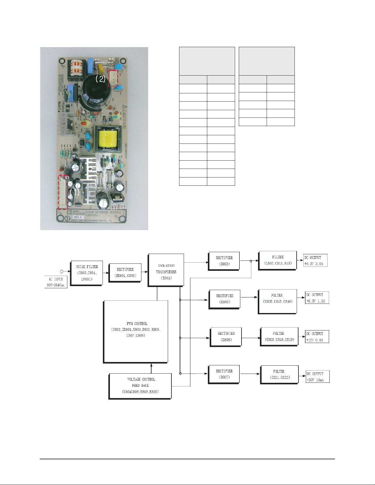
13-2-6 POD SMPS
(1)
J0802(POD SMPS)
↔
P103(Digital B'D)
Pin No Signal
1 ■
N.C
2 +33V
3 GND
4 +12V
5 GND
6 +12V
7 GND
8 +6.5V
9 GND
10 +5V
11 GND
12 +5V
(2)
J0802(POD SMPS)
↔
CN811(MAIN SMPS)
Pin No Signal
1 AC
2 AC
3 5.3V
4 N.C
5 Va
1. Block Diagram
Page 8

Circuit Description
13-8 Samsung Electronics
2. Description of Each Block
- Input Filter Circuit
This consists of a Common Mode Reactor LF801, X-condenser C803, C804, Line by-pass condenser(Y con), C801, C802,
C823, C824 and a lightning conductor, Z801.
The external noise from the AC line and the feedback noise from the internal power are reduced.
- Rectification Circuit
Converts (rectifies) the supplied AC current into DC.
- MAIN SWITCHING Circuit Block
Transmits the energy of the electrolytic capacitor (C805) to the secondary coil, T801 [MAIN TRANS], by turning the MOS-FET
embedded in U802 (5M0565R) on or off for PWM power, and generates a DC output voltage of +5.3V, +6.5V, +12V and +30V.
When the input voltage is supplied, the activation voltage is supplied to Pin 3 of U802, and U802 starts oscillating.
Via the oscillation, the energy is transmitted to the secondary coil, T801.
- DC-DC Circuit Block
The circuit that converts the energy transmitted to T801 via the oscillation of the MAIN SWITCHING U802 into DC voltage.
The +6.5V and +12V voltages are controlled by the Voltage Regulator and the +30V output voltage is controlled by the Turn
Ratio of T801.
Page 9
Circuit Description
Samsung Electronics 13-9
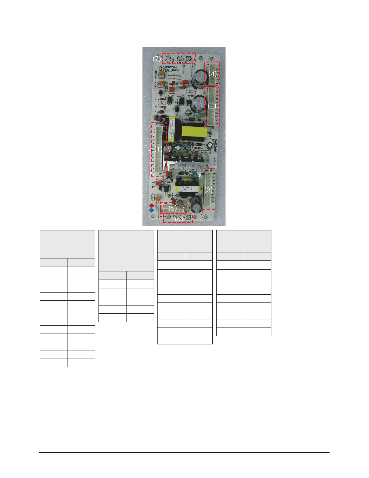
(6) D5.3V, Vg, Ve Test Point
(7) Va, Vset, Vscan Test Point
13-2-7 DC-DC SMPS
(1)
CN809(Main SMPS)
↔
CN3(DC-DC SMPS)
Pin No Signal
1 ■
5.3V
2 Vg
3 RTN
4 RTN
5 RTN
6 RTN
7 RTN
8 Va
9 Va
10 N.C
11 Vs
12 Vs
(4), (5)
CN1, CN6
(DC-DC SMPS)
↔
CN2501(E-Buffer),
CN2701(G-Buffer)
Pin No Signal
1 ■
RTN
2 N.C
3 5.3V
4 N.C
5 Va
(2)
CN2(DC-DC SMPS)
↔ CN5007(Y B'D)
Pin No Signal
1 ■
Vs
2 Vs
3 RTN
4 RTN
5 Vset
6 RTN
7 Vscan
8 RTN
9 Vg
10 5.3V
(3)
CN4(DC-DC SMPS)
↔ CN4000(X B'D)
Pin No Signal
1 ■
Vs
2 Vs
3 RTN
4 RTN
5 Ve
6 RTN
7 RTN
8 Vg
9 5.3V
Page 10
Circuit Description
13-10 Samsung Electronics
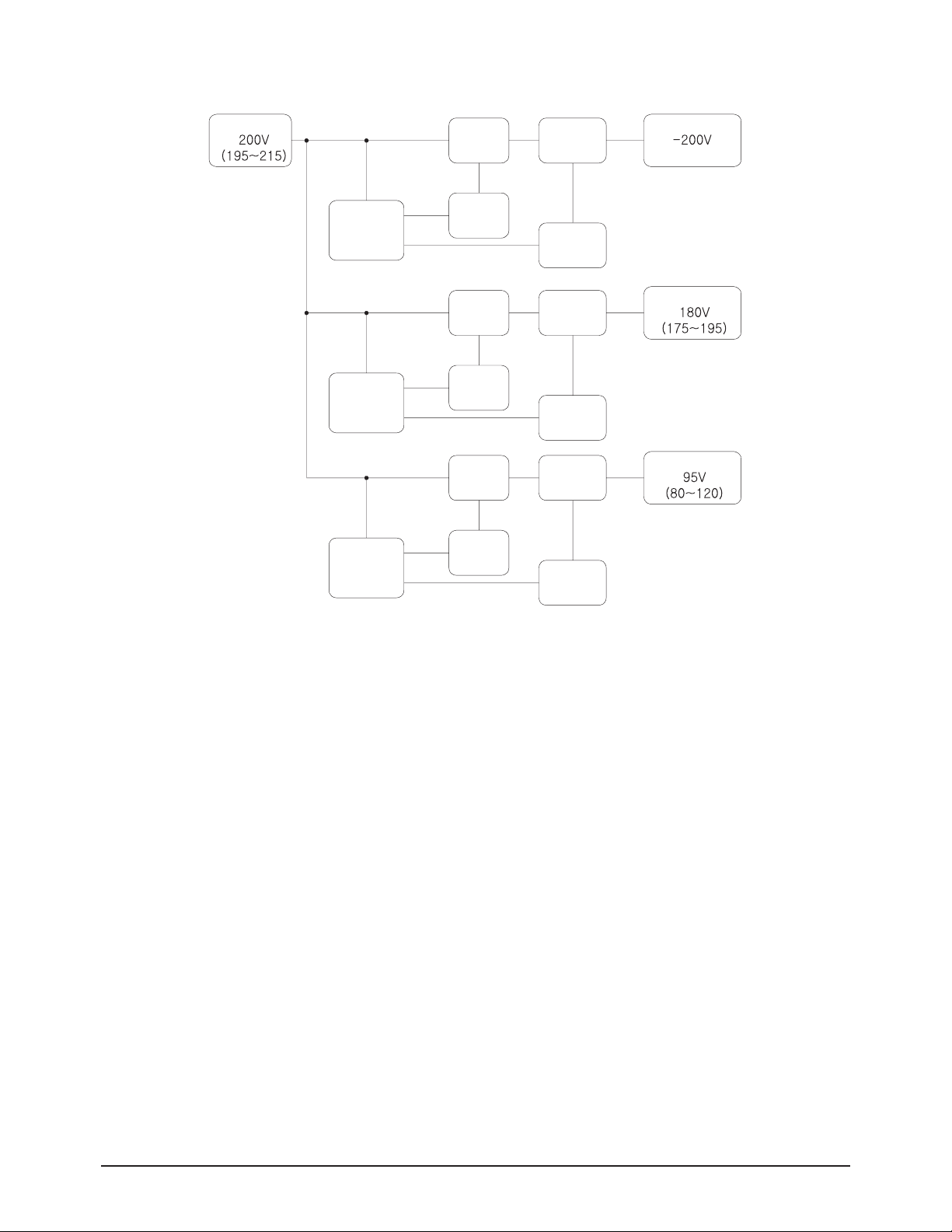
DC DC SMPS receives Vs input (195~215V) from the Main SMPS and the necessary Vscan, Vset and Ve voltages are output to
operate the PDP Module as shown in the block diagram above.
1. Block Diagram
Vs Input Part
Control
and
Switching Block
Control
and
Switching Block
Control
and
Switching Block
Transformer
Auxiliary
Power
Transformer
Auxiliary
Power
Transformer
Auxiliary
Power
Rectification
Block
Feedback
Block
Rectification
Block
Feedback
Block
Rectification
Block
Feedback
Block
Vscan Output
(-175~-220)
Vset Output
Ve Output
Page 11
Circuit Description
Samsung Electronics 13-11
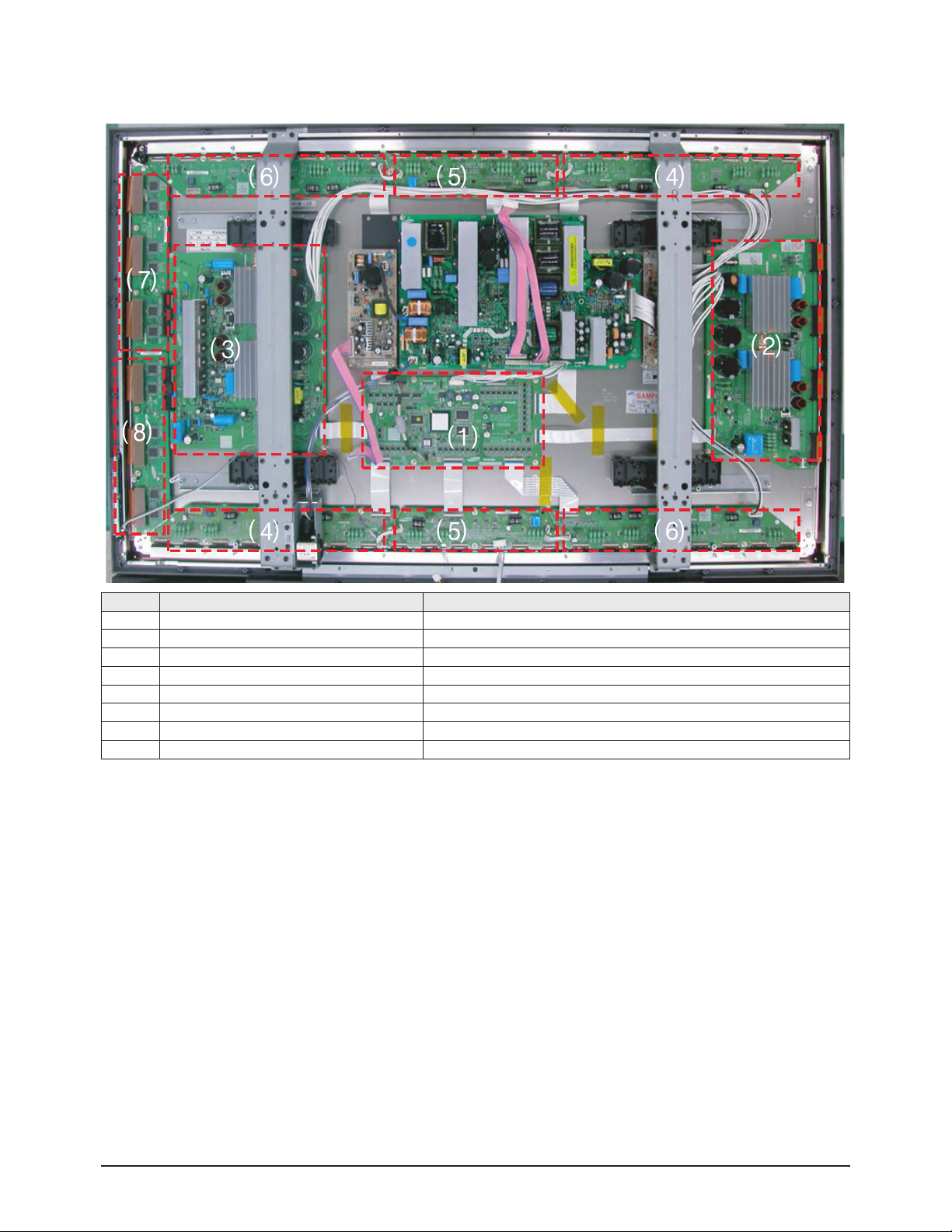
13-2-8 PDP Module
No Assy Name Description
(1) ASSY PDP P-LOGIC BOARD (BN96-02031A) Logic Main Board
(2) ASSY PDP P-X MAIN BOARD (BN96-02024A) X Drive Board
(3) ASSY PDP P-Y MAIN BOARD (BN96-02025A) Y Drive Board
(4) ASSY PDP P-ADDRESS E BUFFER BOARD (BN96-02028A) Buffer Board
(5) ASSY PDP P-ADDRESS F BUFFER BOARD (BN96-02029A) Buffer Board
(6) ASSY PDP P-ADDRESS G BUFFER BOARD (BN96-02030A) Buffer Board
(7) ASSY PDP P-Y BUFF UPPER BOARD (BN96-02026A) Y Buffer Upper Board
(8) ASSY PDP P-Y BUFF LOWER BOARD (BN96-02027A) Y Buffer Upper Board
Page 12
Circuit Description
13-12 Samsung Electronics
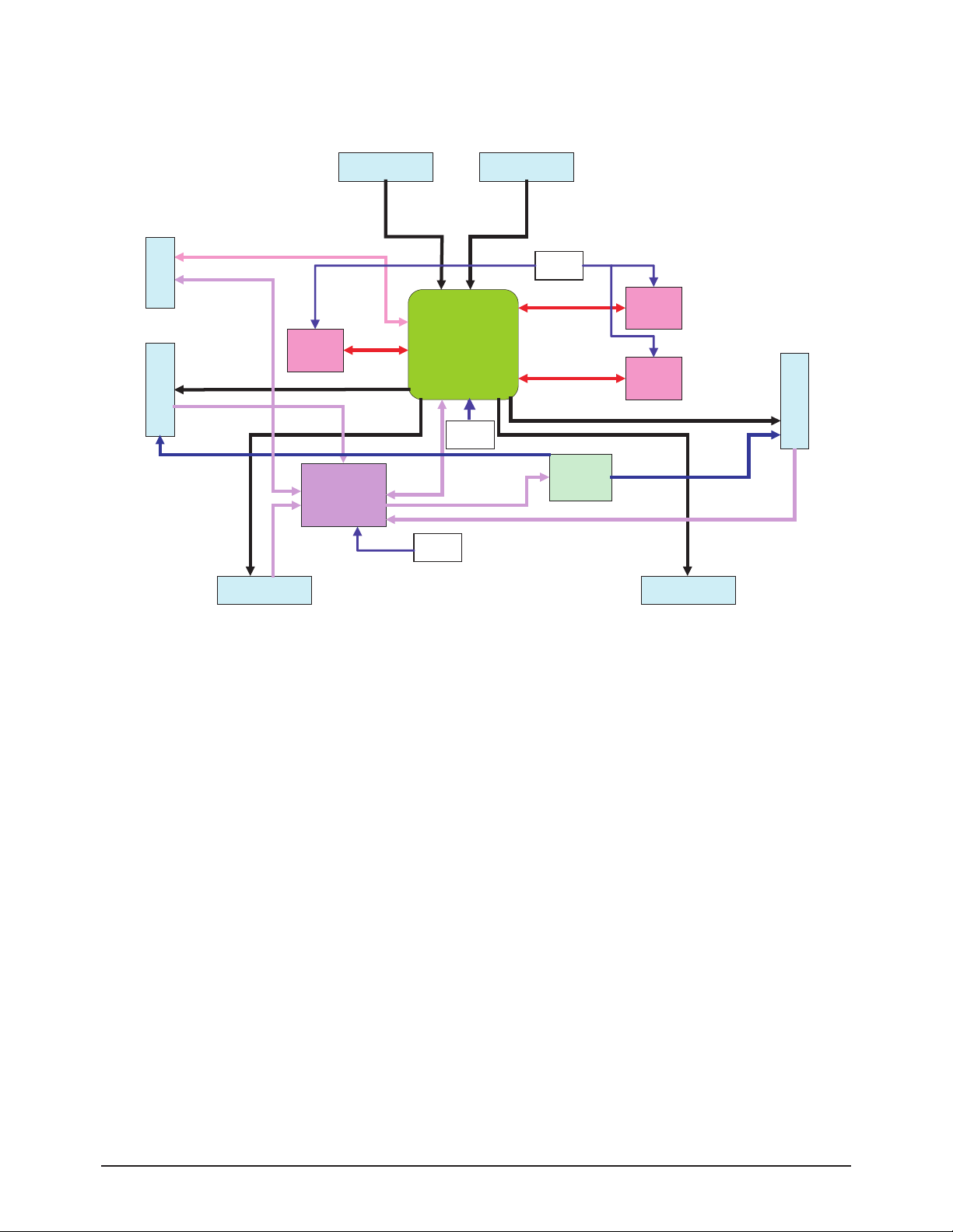
1. Logic Block
■ Logic Block Diagram
4pin (I2C)
SDA, SCL
LVDS
SIGNAL
10Pin(Power)31Pin LVDS
RELAY_EINT
AC-OFF-EINT
Vs-ON
60MHz
TX, RX
50pin Connector
Y-MAIN
CONTROL
SIGNAL
ADC 4bit
R,G,B : 16bit
CLK A, B
BLK, POL, STB
60pin Connector 60pin Connector
DDR
(FA)
ADC 1bit
MICOM
(ASIC 816P)
CONTROL
SIGNAL
30MHz
SPS-NIRB
74MHz
ASIC
nRESET
DATA : 32bit
ADDR : 12bit
DQS, CLK, nCLK
DRIVE
RESET
DDR
(MA)
DDR
(MB)
X-MAIN
CONTROL
SIGNAL
ADC 3bit
R,G,B : 16bit
CLK A, B
BLK, POL, STB
30pin Connector
Page 13
Circuit Description
Samsung Electronics 13-13
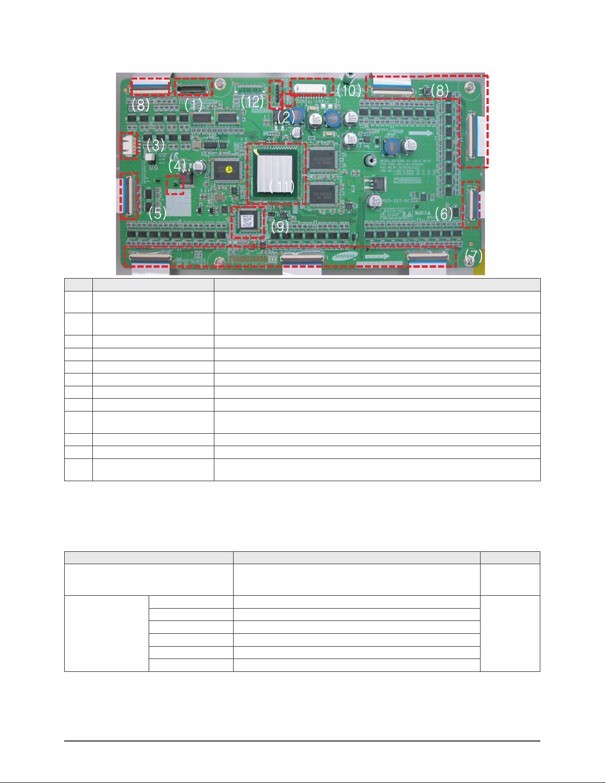
■ A name of main part of Logic Board and vocabulary.
Item Name
Description
①
LVDS Connector
The connector to receive the RGB, H, V, DATAEN and DCLK signals that have been LVDS encoded through the
main board.
②
Operating Status LED (LED2001)
The LED that shows whether the Sync and Clock signal is properly supplied to the logic board (Normal
Status:Blinks at 0.8 second intervals)
③
I2C Connector (Debug only) The connector for the Key Scan board that checks and controls the 512K data.
④
V-TOGG TP for V Sync Check
⑤
Y Connector The connector to output the control signal for the Y drive board.
⑥
X Connector The connector to output the control signal for the X drive board.
⑦
CN2006, CN2007, CN2008 The connector to output the address data and the control signal to the E,F and G-buffer board of BOTTOM.
⑧
CN2009, CN2010, CN2011 The connector to output the address data and the control signal to the E,F and G-buffer board of TOP.
⑨
ARM-PROCESSOR
512K including the Gamma Table, APC Table, drive waveform timing and other options is saved to internal
flashmemory.
⑩
Power Connector The connector to receive power (5V, 3.3V) for the Logic board.
⑪
ASIC CHIP The main processor that generates and outputs the logic drive signal and the address data.
⑫
MICOM LOADING 5PIN CONNECTOR
(Debug only)
The connector to load the Micom drive program. The program is loaded by connecting to the GA-WRITER.
■ About Logic Board
The Logic Board consists of a Logic Main board, which processes the main signal input through LVDS and creates the address
driver output and X,Y drive signals, and a Buffer board, which buffers the output signal and outputs the signal to the Address Driver
IC (TCP IC).
Logic Board Function Remark
Logic Main
- Video Signal Processing (W/L, error diffusion, APC)
- Outputs the Address Driver Control and Data Signals to the Buffer board.
- Outputs the XY Drive Board Control Signal
Buffer Board
Lower E Buffer board Outputs data and control signals to the bottom left TCP IC.
Top and bottom
Symmetry design
Lower F Buffer board Outputs data and control signals to the bottom center TCP IC.
Lower G Buffer board Outputs data and control signals to the bottom right TCP IC.
Upper E Buffer board Outputs data and control signals to the Top right TCP IC.
Upper F Buffer board Outputs data and control signals to the top center TCP IC.
Upper G Buffer board Outputs data and control signals to the top left TCP IC.
Page 14
Circuit Description
13-14 Samsung Electronics
■ Major Check Points and Waveforms
- The waveform during a Normal Operation
When the PDP set and the Logic Board are properly operating, the Operation Status LED blinks at approximately 0.8 second
interval as shown in Figure 1.
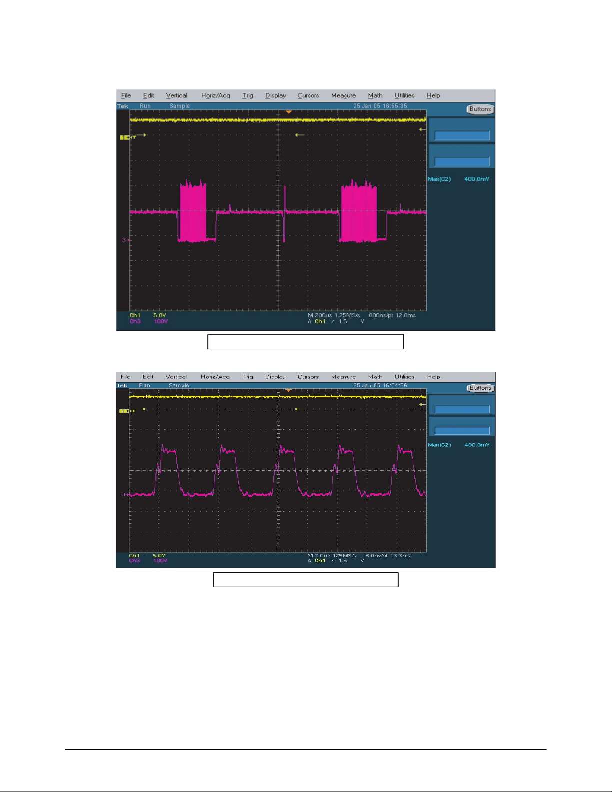
If the set is out of order, check the Operation Status LED first, and check that the output waveform is normal using an
oscilloscope.
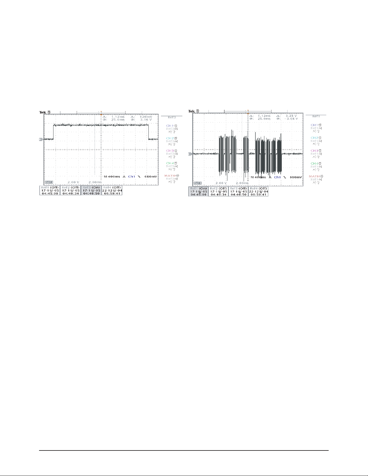
Check if the waveform is the same as shown in Figure 2 by connecting the oscilloscope to the No. 12 TP in Figure 1. Check if
the waveform is the same as in Figure 3 by connecting the oscilloscope to the connector that is connected to the Buffer board.
If the measured waveform is different from the following waveforms, the board must be replaced.
To check the waveforms, refer to the following waveform patterns.
Figure 2. Normal V-SYNC Output Waveform Figure 3. Normal Address Data Output Waveform
Page 15

Circuit Description
Samsung Electronics 13-15
1. X, Y Control Block
■ Drive Circuit Definition
The Drive Circuit is a circuit that generates a waveform (high-voltage pulse) for the X and Y electrode group of the panel's external
port so as to control the panel. The high-voltage switching pulse is generated through the combination of the IC HYBRID (Drive
block + IGBT) and FET.
■ Drive Circuit Mechanism
A picture is displayed on the PDP by applying voltage to the X, Y and ADDRESS electrodes of each pixel according to the appropriate condition. The drive waveform applied to 42HD V4 is of the ISSS (ISSS: Interweaving Scan and Selective Sustain with Scan
IC) type and has IDS (InDependent Sustain) in the Scan section unlike the existing ADS. Discharges within a PDP pixel can be
classified into 3 types:
① Address Discharge: To form a wall voltage within the pixel by giving information (applying DATA voltage) to the pixel to be lit.
② Sustain Discharge: Sustain Discharge is a display section that voluntarily maintains the discharge of the pixels whose wall
voltage has been formed by the Address Discharge. (Optical output for displaying a picture is generated).
③ Erase Discharge: To selectively perform Address Discharge for each pixel, all pixels on the panel should be in the same status
(the wall electric charge status and space electric charge status must be the same). Therefore, the Erase
Discharge section is an important component for guaranteeing the drive margin, and is implemented by
various methods such as applying a log waveform. However, the current 42HD V4 has adopted a wall voltage
control through an RA (Repeated Auto-quenching) reset that separates the discharge area and performs
switching to perform an efficient erase operation, while the gradient was the same in the RAMP section in the
existing approach.
1) Address Discharge
A discharge that is caused by the difference between the plus electric potential (Va apply voltage of 65~70V + Positive Wall
Charge) of the electrode and the negative electric potential (Applied GND Level + Negative Wall Charge) of the Y electrode. The
Address discharge forms a wall voltage within the pixel to display color (to be discharged) before the Sustain Discharge period.
That is, the pixel whose wall charge has been formed by the Address Discharge forms a Sustain Discharge vis the following
Sustain pulse.
2) Sustain Discharge
A Sustain Discharge is a Self-Sustaining Discharge formed by the accumulation of the electric potential of the Sustain pulse (generally 200 ~ 210 Volt) alternating over the X and Y electrodes during the sustain period, and the wall charge depending on whether
the pixel has previously been discharged or not. That is, it is controlled by the memory characteristics, one of the basic characteristics of the AC PDP (in that the past operating conditions determine the current status). That is, if a wall voltage exists on the pixel
(if the pixel is on), a discharge is formed again because the applied voltage, which is the sum of the following applied Sustain voltage and the wall voltage, is higher than the discharge threshold voltage. If no wall voltage exists on the pixel (if the pixel is off), a
discharge will not occur because the Sustain voltage is not higher than the discharge threshold voltage. The Sustain Discharge
period is the period for generating actual optical output so as to display a picture on the PDP screen.
3) Erase Discharge
The purpose of a Reset (Erase) Discharge is to create uniformity of the wall voltage within all panel pixels. It evens the wall voltages regardless of the Sustain Discharge in the previous stage. The Erase Discharge has to remove the wall voltage introduced by
the Sustain Discharge by supplying ions or electrons by a discharge. When the wall voltage is removed through a discharge, the
time when the reverse polarity is applied to the wall voltage (fine width erasing) is to be limited or ions or electrons are to be supplied by a weak discharge (low voltage erasing) so as to prevent a wall charge in reverse polarity.
There are 2 known weak discharge (low-voltage) erase methods. 1) A log waveform adopted by F company and 2) a weak erase
discharge via a ramp waveform adopted by Matsushita and other companies. Both methods control the externally applied voltage
by the difference of the wall voltage of the pixel by applying the rising gradient of the erasing waveform slowly, because the discharge begins when the sum of the existing remaining wall voltage and the rising waveform voltage exceeds the drive threshold
voltage. In addition, a weak discharge is introduced, because the applied voltage is low.
Page 16
Circuit Description
13-16 Samsung Electronics
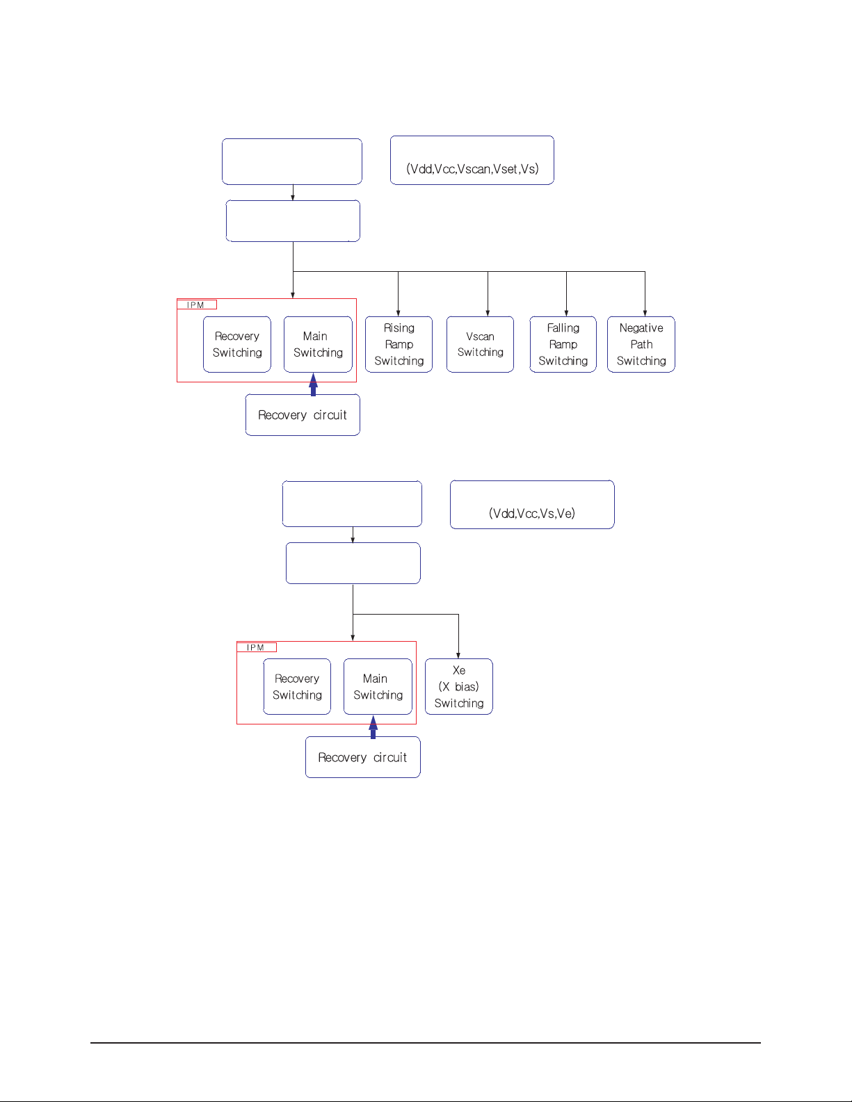
■ Drive Circuit Operating Block Diagram
- Y Drive Board
- X Drive Board
■ Requisite Components Necessary for Drive Board Operation
- Power : Supplied from the power board. The optimal value may differ from the following:
a) Vs : 205V - Sustain
b) Vset : 195V - Y Rising Ramp
c) Ve : 100V - Ve bias
d) Vscan : -190V - Scan low bias
e) Vnf : -175V - Y falling Ramp (Created by the DC-DC power block of the Y Drive board)
f) Vsc_h : -70V - Scan high bias (Created by the DC-DC power block of the Y Drive board)
g) Vdd : 5V - Logic signal buffer IC and IPM
h) Vcc : 15V - Gate drive IC ¹× IPM
- Logic Signal : Supplied by the Logic board. Gate signal of each switch
Logic Signal Input Part
Logic Signal Buffer
Logic Signal Input Part
Power Input Part
Power Input Part
Logic Signal Buffer
Page 17
Circuit Description
Samsung Electronics 13-17
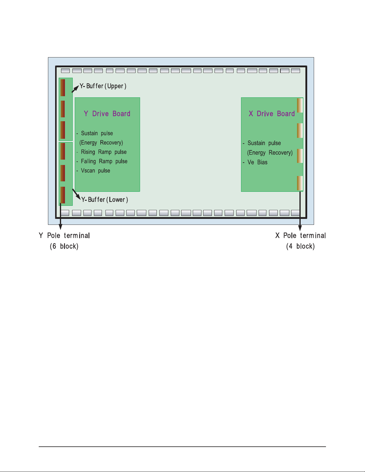
■ Drive Circuit Architecture and Function Description
- Description of the function of each board
1) X Drive Board
This is connected to the X port part of the panel. 1) Sustain voltage waveform (including ERC) is output, and 2) Ve bias in the Scan
section is maintained.
2) Y Drive Board
This is connected to the Y port part of the panel. It outputs 1) Sustain voltage wave form (including ERC), and 2) Y Rising, Falling
Ramp waveform, and maintains 3) Vscan bias.
3) Y Buffer Board (Upper, Lower)
This board supplies the Scan waveform to the Y port and consists of Upper and Lower boards. For an HD grade unit, 6 scan
driver ICs (TEXAS INSTRUMENT SN755867APZP: 64 outputs) are mounted on the board.
Page 18
Circuit Description
13-18 Samsung Electronics
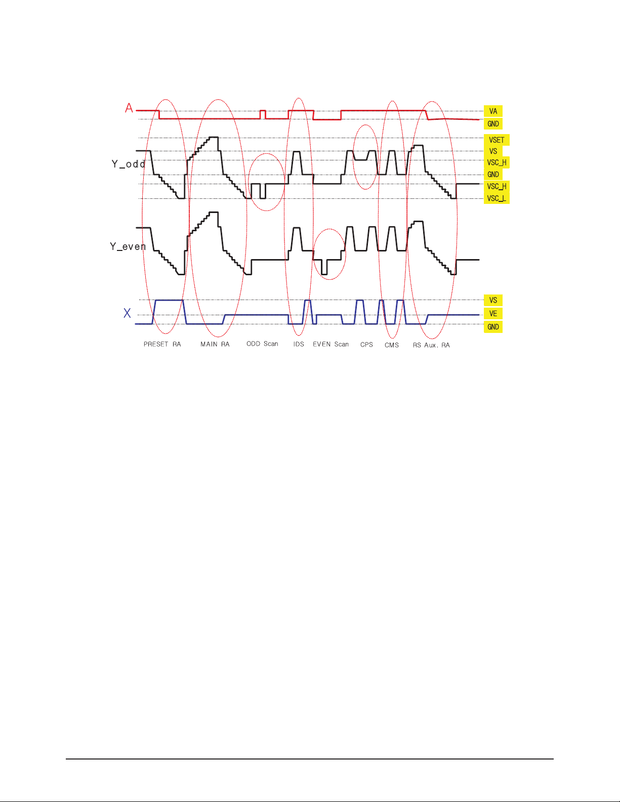
■ Drive Waveform Specifications
- Drive Waveform
- Description of the function of each pulse
1) Y Preset RA Pulse
This is supplied to the first sub-field and erases the discharge status of the previous subfield.
2) Y Main RA Pulse
During the Y Rising Ramp section, approximately 300V~350V (Vscan-h + Vset) of external voltage is supplied to the Y electrode,
and a weak discharge is started when each gap voltage is equal to the discharge start voltage. While maintaining the weak discharge, as a whole, negative wall charges are accumulated on the Y electrode and positive wall charges on the X electrode and
the address electrode.
During the Y Falling Ramp section, the negative wall charges accumulated on the Y electrode by the approximately 105V of X bias
are used to erase the positive wall charges on the X electrode, and the address electrode maintains most of the positive wall
charges accumulated during the (0V) Rising Ramp section preparing for the next address discharge.
3) Y Scan Pulse (Odd/Even)
A scan pulse classifies the Y electrode into Odd and Even lines and selects FPC output electrodes sequentially (one line-at-atime). At this time, Vscan is called the Scan Bias Voltage.
A Vscan voltage of approximately -175 Volt (Vsc_1) is supplied to the electrode lines. For the other lines, -56 volt (Vsc_h is higher
than Vscan-l by 120V) is supplied. However, negative wall charges are accumulated on the Y electrode by the Ramp pulse, and
positive wall charges are accumulated on the address electrode, and the voltage applied to the cells, to which the Address pulse
(70V~75V) has been applied, becomes higher than the discharge voltage. An address Discharge occurs as a result. Since the
Scan and Data pulse is applied one line at a time as above, the address time of PDP is very long.
4) IDS Pulse (InDependent Sustain Pulse)
Since an Odd Scan is performed first, the Odd line output sustains optical twice during the IDS section. At this time, a Sustain
Discharge does not occur for the Even line because the Even line is not scanned.
5) CPS Pulse (ComPare Sustain Pulse)
By floating the Odd line that caused the Sustain Discharge in the IDS section to the Vscan-h level, and introducing the Sustain
Discharge only for Even lines, it compensates for the optical output difference between the Even and Odd lines.
6) CMS Pulse (ComMon Sustain Pulse)
Actual optical is output during the common Sustain Discharge section.
Page 19
Circuit Description
Samsung Electronics 13-19
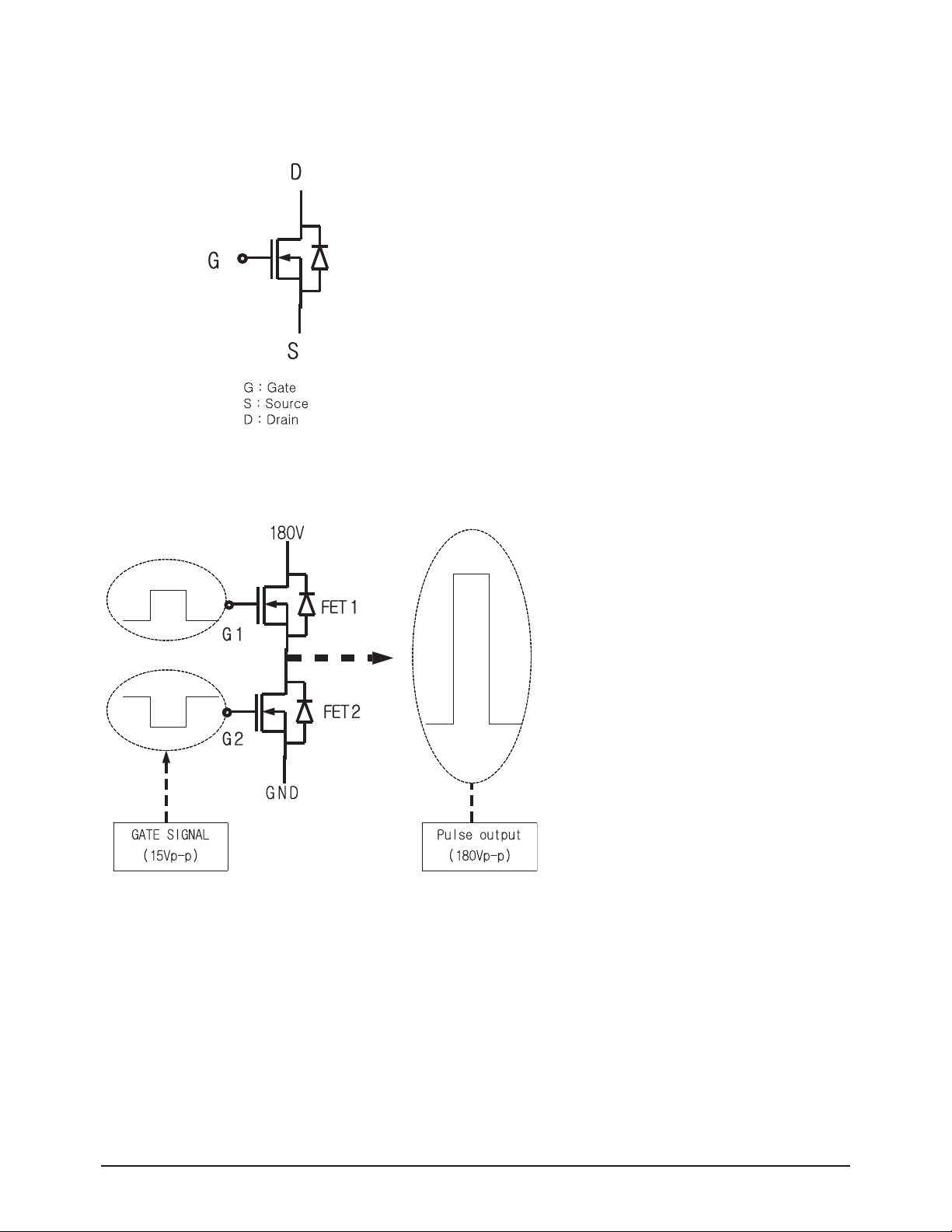
■ Mechanism of the FET Operation and High-Voltage Switching
Mechanism of the FET Operation
1) When the signal is output to the gate, (positive electric
potential) FET short circuits
(i.e. Conductor of resistance 0)
2) When no signal is output to the gate (GND), FET changes
to an open circuit (i.e. an insulator of resistance ∞).
High-Voltage Switching of the FET Operation
1) When no signal is applied to G1, FET1 is
opened and when the signal is applied to G2,
FET2 short circuits, GND is output via the output
terminal.
2) When a signal is applied to G1, FET1 short cir
cuits and when no signal is applied to G2, FET2
is opened, and 180V is output via the output
terminal.
Page 20
Circuit Description
13-20 Samsung Electronics
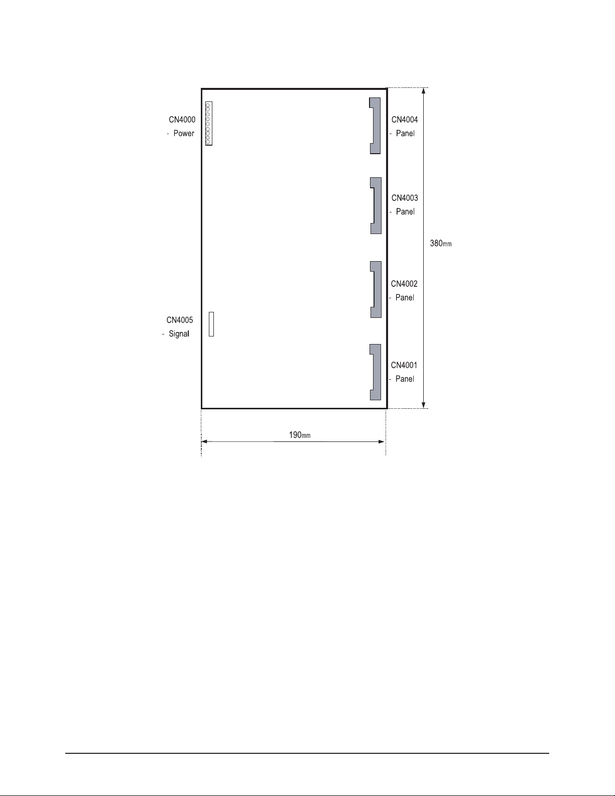
■ Drive Board Connector Layout
1) X-Main
Page 21
Circuit Description
Samsung Electronics 13-21
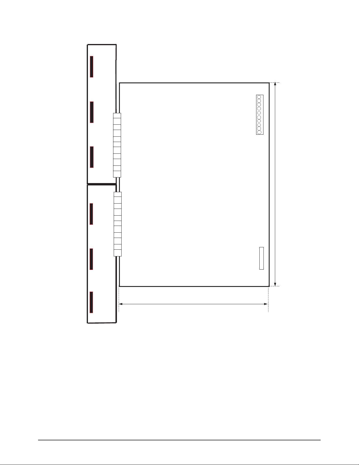
2) Y-Main
CN5401
-Panel
CN5402
-Panel
CN5403
-Panel
CN5407
CN5007
-Power
CN5009
320mm
CN5501
-Panel
CN5502
-Panel
CN5503
- Panel
CN5507
CN5010
CN5008
-Signal
265mm
Page 22
Circuit Description
13-22 Samsung Electronics
■ Troubleshooting the Drive Board
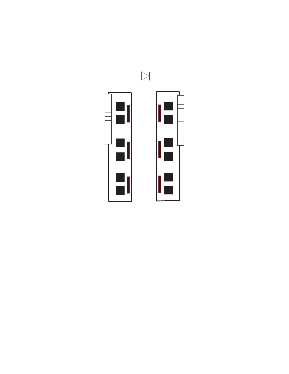
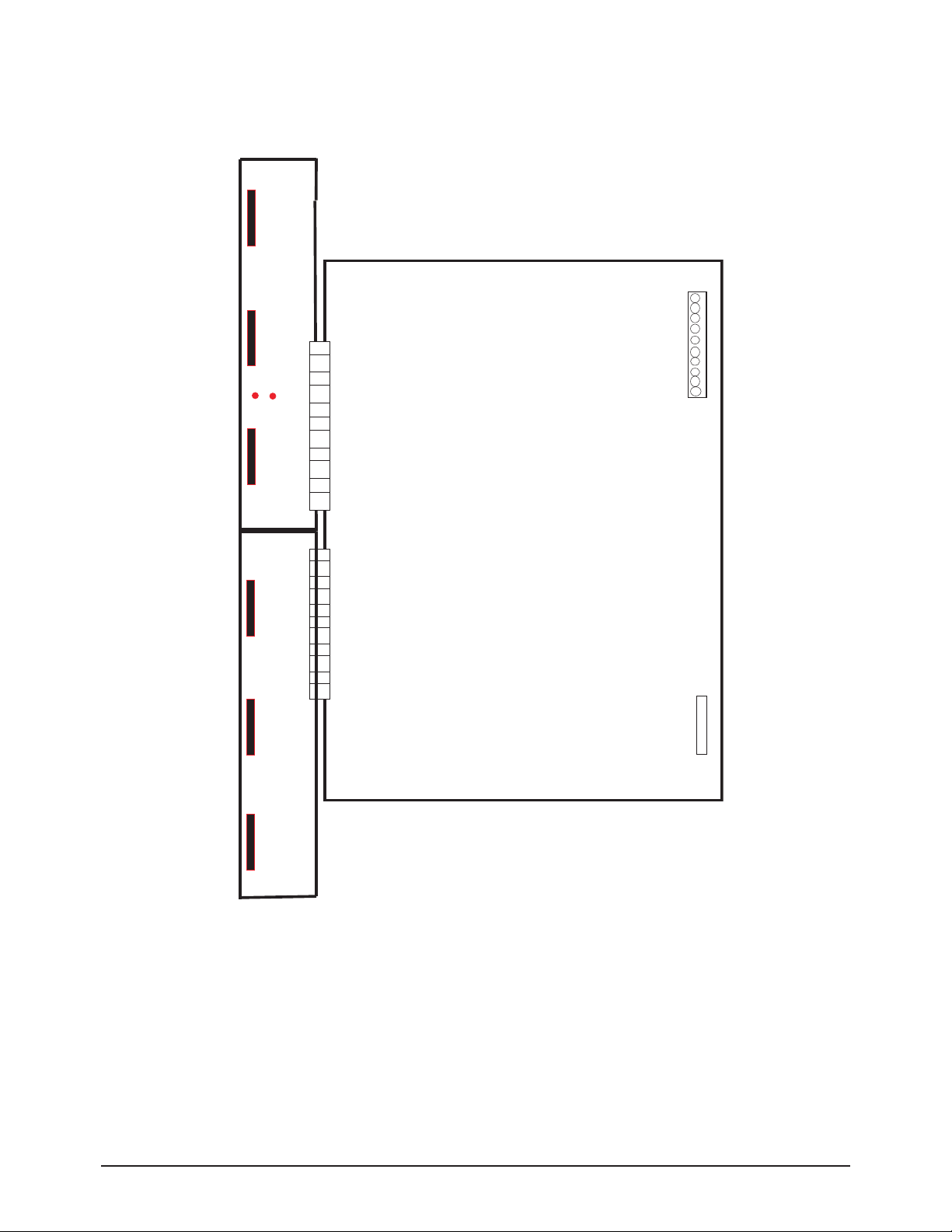
1) Y Buffer
- To check whether the Y Main board is properly working, check the operation of the Y Buffer first.
- Separate the connector of the Y Buffer from the Y Main board.
- Check OUTL and OUTH and confirm that the forward voltage reduction is between 0.4V ~ 0.5V.
UP - CN5407 1~10pin - OUTH / 11~33pin - OUTL
LOW - CN5507 50~41pin - OUTH / 40~17pin - OUTL
- In addition, the resistance between the points must be higher than a few kΩ .
OUTL OUTH
OUTL
OUTH
<Y buffer UP>
OUTL
OUTH
<Y buffer LOW>
Page 23
Circuit Description
Samsung Electronics 13-23
2) Y Main
- Connect the Y Main and Y Buffer, and confirm that the output from TP(CN5410, CN5411) of the Y Buffer UP is the same as
#Attachment 1 when the power is supplied.
CN5410
CN5411
Page 24
Circuit Description
13-24 Samsung Electronics
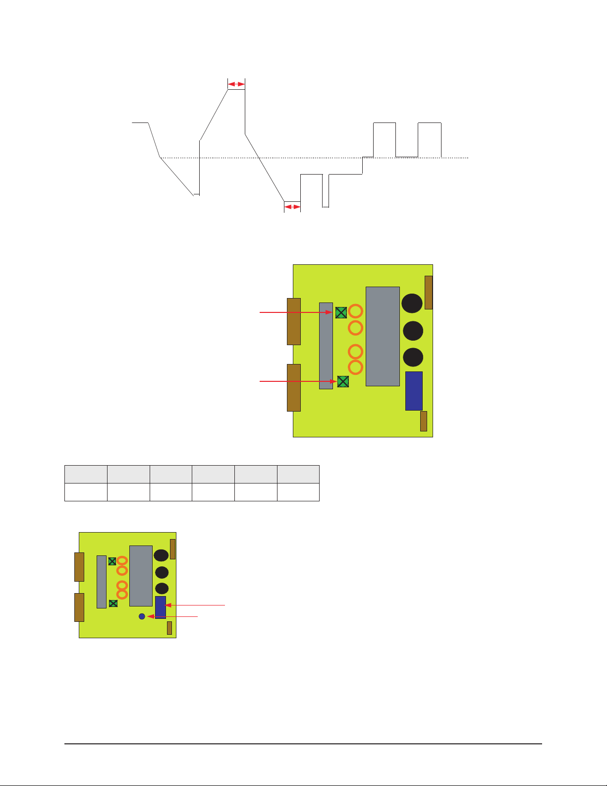
▶ Adjust the drive waveform so that the main reset (Rising: 100 usec, Falling: 40 usec) are the same as those in the figure.
※ The Vsc_h and Vnf voltages are controlled by the DC-DC power part of the Y Main board.
<Voltage Adjustment Specifications>
100us
40us
Vset Vs Vsc_l Vsc_h Ve Va
200V 205V -175V -56V 105V 70V
Rising Ramp
Falling Ramp
Rising Ramp Variable resistor
1 0 0 us
...
4 0 u s
IPM
Falling Ramp Variable resistor
YMainBoard
DC-DC
Vsc_h TP
YMainBoard
DC-DC
Page 25
Circuit Description
Samsung Electronics 13-25
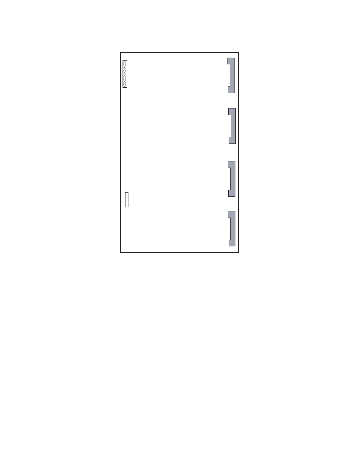
3) X
- Check that the output of X-Out of the X board follows the waveform of #Attachment 2 when the power is supplied.
XOUT
Page 26
Circuit Description
13-26 Samsung Electronics
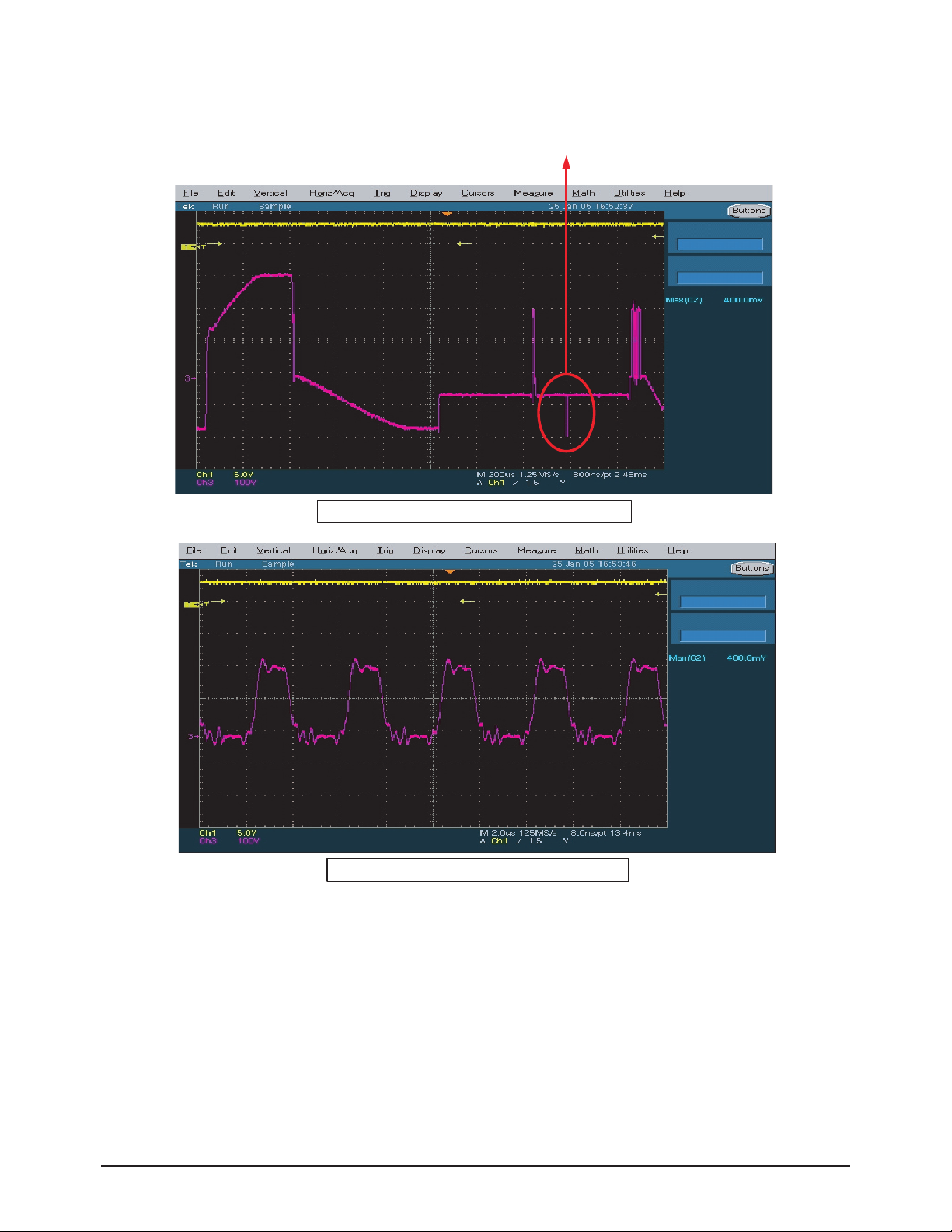
※ Attachment 1
■ Y Output Waveform
The Scan Waveform Must Be Observed
Y Output Waveform (200us/div, 100V/div)
1us/div, 100V/div (Sustain Waveform)
Page 27
Circuit Description
Samsung Electronics 13-27
※ Attachment 2
■ X Output Waveform
X Output Waveform (200us/div, 100V/div)
2us/div, 100V/div (Sustain Waveform)
Page 28
Circuit Description
13-28 Samsung Electronics
13-3 New Circuit Description
13-3-1 Power Saving Modes (Standard, Automatic, Super Power Saving)
1. Objective
To enhance a sensible visual quality by maintaining an appropriate screen brightness according to the ambient brightness and to
reduce power consumption.
2. Circuit Architecture
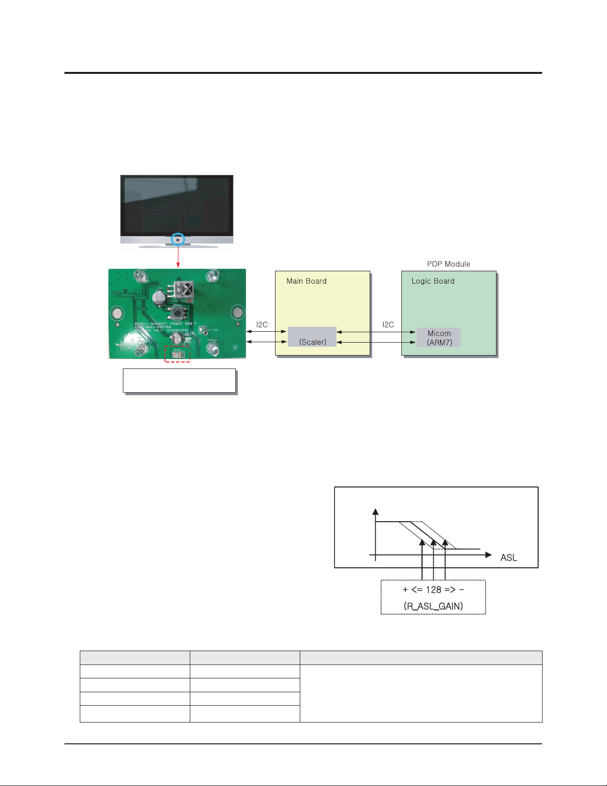
The CPU S3C2800 of the Video Board monitors the current ambient brightness (in Lux units), stored in the Ambient Light Sensor
of Power Assy., which is attached at the front of the PDP, at given intervals through SMBUS communication (identical to I2C) and
controls the PDP module to operate at the appropriate luminance level.
3. Descriptions of Each Mode
1) Standard Mode
Standard Mode is set as standard visual quality.
2) Auto Power Saving Mode (Ambient Light Sensor)
This uses the TAOS 4 pin TSL2550 and is currently being used in
LCD TVs. It also uses SMBUS, which is the same type as I2C, for
communication. The Ambient Light Sensor can detect up to 1846
Lux in normal mode. The data of the sensor can be measured for
Lux operations once every 800ms.
Control is implemented by using R_ASL_GAIN. The number of
sustain pulses moves left or right as shown in the figure on the right.
For a low gradation condition, the change by R_ASL_GAIN has
been minimized considering the degradation of the visual quality.
That is, the Auto Power Saving mode screen controlled by the
ambient light sensor aims at normal video of medium gradation.
※ The following values are for a normal air signal with 80 Watt attenuation at maximum
Detected Lux R_ASL_GAIN (Address 0xE9) Remarks
0 ~ 8 250
- Read the Lux value once per second and change it the target
R_ASL_GAIN value by 5 per second according to the changed Lux
value.
- If more than 3 communication errors or saturation (count1>count0) is
detected, the default value is set (R_ASL_GAIN=128).
9 ~ 22 210
23 ~ 35 170
Else 128 (default)
S3C2800
Ambient Light Sensor
(TSL2550 Lux Calculation IC)
Number of Sustain Pulses
Page 29
Circuit Description
Samsung Electronics 13-29
3) Super Power Saving Mode
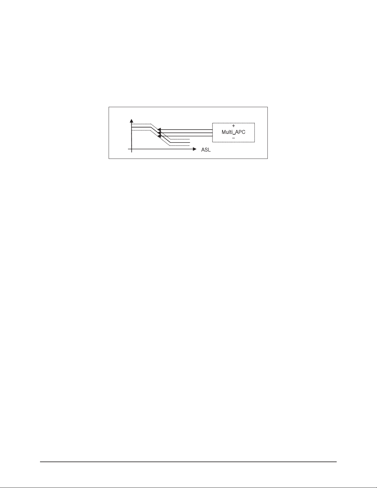
This uses the Multi APC function of the PDP module, and aims at reducing power consumption more than 100 W for the white
pattern, which is similar to the power consumption reduction of other manufacturers.
- Concept of Multi APC
: Controls the number of sustain pulses according to the ASL (Average Signal Level) by R_P_Lower_Gain value.
In the PDP Logic, R_Multi_APC is set to 0X01, Multi_APC operates, and R_P_CM_Gain_SW is set to 0X01 so that the
upper and lower limits of the APC Table can be shifted by adjusting the R_P_Lower_Gain value only.
Therefore, the sustain pulse is controllable for the white pattern, even though it was formerly not controllable.
※ Caution: The Super Power Saving Mode screen is darker than that of Standard Mode.
Number of Sustain Pulses
Page 30

13-30 Samsung Electronics
MEMO
 Loading...