

Samsung G74, CKB5237, CKB5237L, CKB7227L Schematic
CKB5237L/7227L 11-1
11 Schematic Diagrams
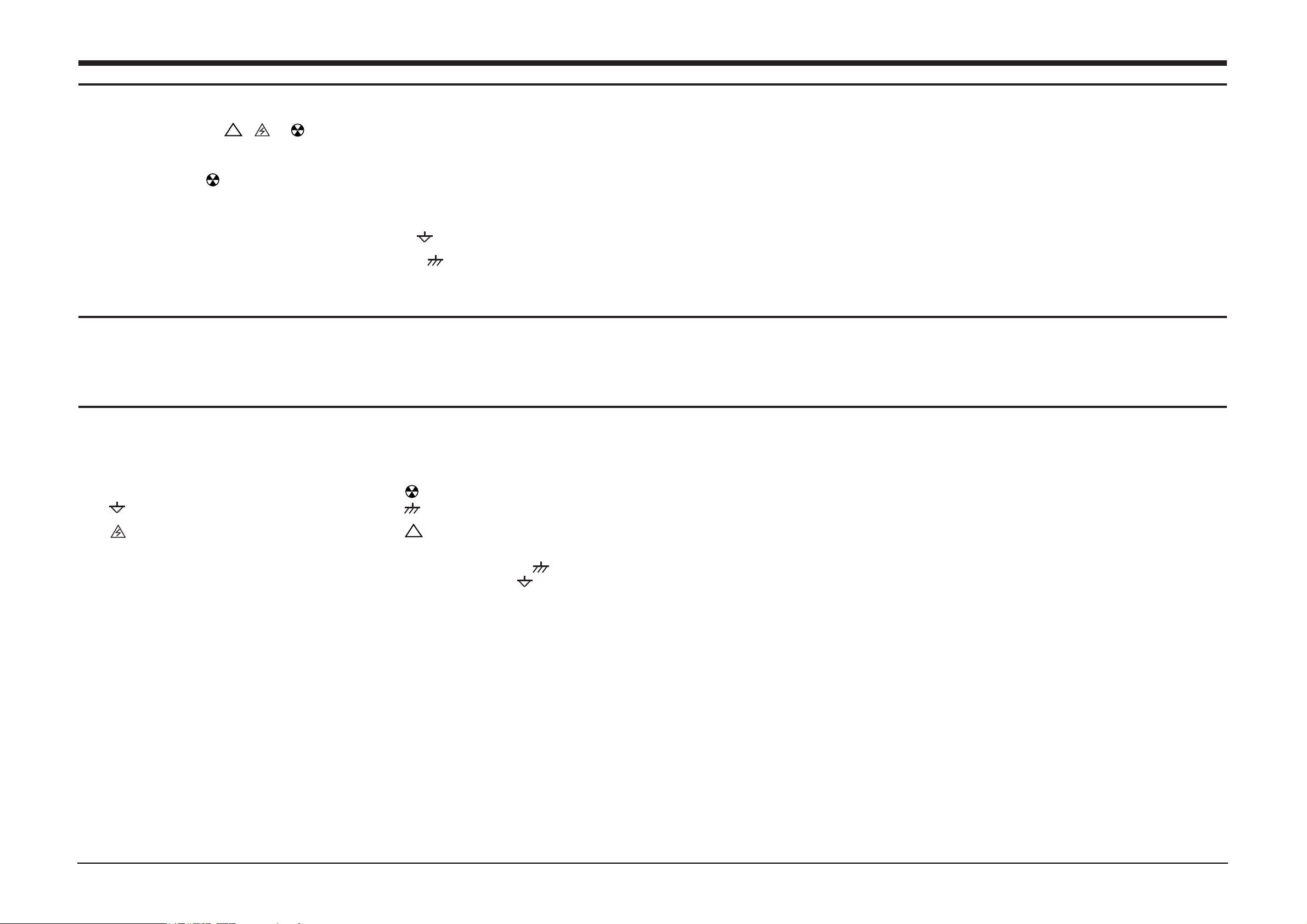
11-1 Cautions
1. The areas marked with a , or on the schematic diagram designate components which have special characteristics important for safety.
Replace these parts only with parts identical to those in the original circuit and those specified in the parts list.
Before replacing any of these components, carefully read the ÒProduct Safety Notice.Ó
2. Areas marked with a on the schematic diagram designate controls which have been sealed for safety during manufacturing.
If these controls need adjustment, they must be replaced with new controls and then sealed after their adjustment.
3. When taking measurements, pay special attention to the following:
1) Do not use your instrument between primary ground (symbol ) and secondary circuit.
2) Do not use your instrument between secondary ground (symbol ) and primary circuit.
11-2 Notes
1. Resistance is shown in OHM. K = 1,000, M = 1,000,000 and the rated power of resistors not noted in the schematic diagram is 1/4W.
2. Capacitance is shown in µF. Capacitances not otherwise noted are shown in pF (1µF = 1,000,000 pF). Rated voltage of condensers
not otherwise noted in the schematic diagram is 50 V.
11-3 Abbreviations and Symbols
MO R-Metal Oxide WW R-Wire Wound
FU Fusible C R-Composition
CM R-Cement MPP Metal Polypropylene
MP C-Metalized Polyester T C-Tantalum
P C-Polyester Can emit X-radiation
Hot Ground Cold Ground
Electrostatically Sensitive Device Provides special safety
(ESD) considerations
1. The secondary voltage is read with an SSVM from the indicated point to a cold ground ( ).
The primary voltage is read with an SSVM from the indicated point to a hot ground ( ).
2. This schematic diagram is subject to change without notice.
!
!
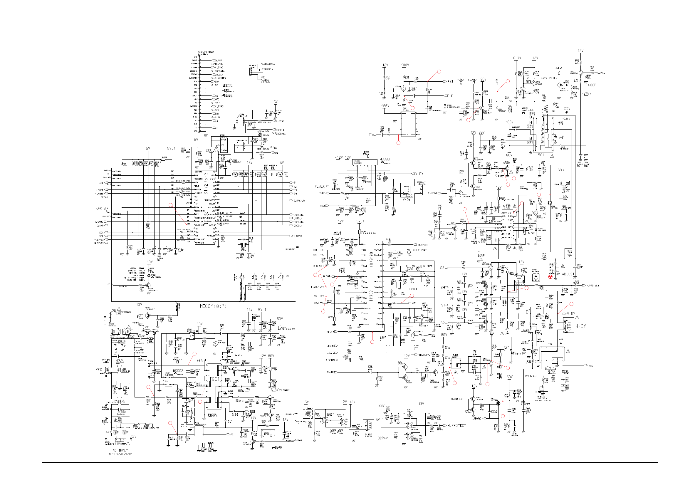
11 Schematic Diagrams
11-2 CKB5237L/7227L
11-4 Main Schematic Diagram
15" ONLY
17" ONLY
R501
C455_5
C465_7
Q417_7
R467_7
Q500_7
C543_7
C540_7
C538
R502_7
R506
R443
R425
C522_7
C537_7
R302
R451
R450
R310
R414
R409
R417
L406
C456
R535
C434 C458
C432
L402
C422
L401
R517
C419
L501
D524_7
R201_7
R613
R503_7
R504_7
R505_7
R500_7
R444_7
R441_7
R315
4
2
1
3
29
5
7
8
6
10
9
11
12
13
14
16
15
19
20
22
23
21
28
26
27
24
25
11 Schematic Diagrams
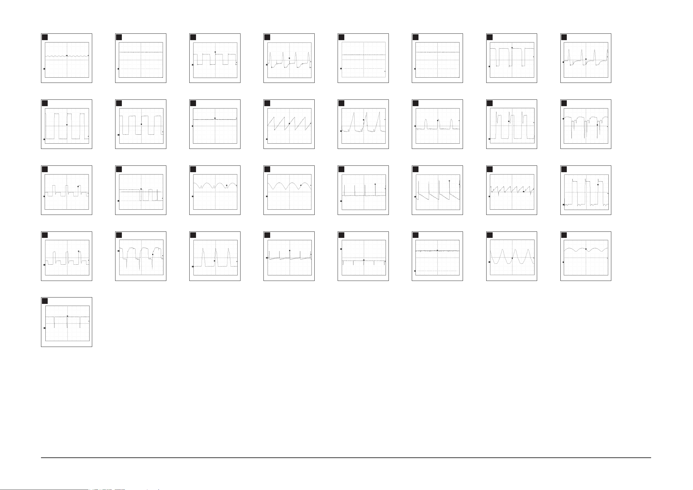
CKB5237L/7227L 11-3
14 V (T601, #1), 110V
CH1 P-P = 14 V CH1 RMS = 142.6 V
1
12.0 V (IC302, #28)
CH1 P-P = 12.0 V CH1 RMS = 6.912 V
5
928 mV (IC302, #16)
CH1 P-P = 928 mV CH1 RMS = 320.8 mV
9
128 V (Q411, Drain)
CH1 P-P = 128 V CH1 RMS = 63.3 V
13
DC V (IC602, #3)
CH1 P-P = DC V CH1 RMS = DC V
2
8.80 V (IC302, #26)
CH1 P-P = 8.80 V CH1 RMS = 6.176 V
6
2.56 V (IC302, #12)
CH1 P-P = 2.56 V CH1 RMS = 820 mV
10
1.016 kV (Q406, Collector)
CH1 P-P = 1.016 kV CH1 RMS = 316.0 V
14
292 V (T601 #5), 110V
CH1 P-P = 292 V CH1 RMS = 181.6 V
3
3.68 V (C612, –), 110V
CH1 P-P = 3.68 V CH1 RMS = 840 mV
4
DC V (T601, #2), 220V
CH1 P-P = DC V CH1 RMS = DC V
1
DC V (IC602, #3), 220V
CH1 P-P = DC V CH1 RMS = DC V
2
444 V (T601, #5), 220V
CH1 P-P = 444 V CH1 RMS = 354.2 V
3
3.80 V (C612, –), 220V
CH1 P-P = 3.80V CH1 RMS = 902 mV
4
640 mV (IC302, #24)
CH1 P-P = 640 mV CH1 RMS = 2.908 V
7
124.8 V (T401, #1)
CH1 P-P = 124.8 V CH1 RMS = 66.16 V
11
64 V (L402_7, S)
CH1 P-P = 64 V CH1 RMS = 126.0 V
15
3.12 V (IC302, #23)
CH1 P-P = 3.12 V CH1 RMS = 3.620 V
8
10.0 V (Q406, Base)
CH1 P-P = 10.0 V CH1 RMS = 1.672 V
12
76 V (L402_7, F)
CH1 P-P = 76 V CH1 RMS = 127.2 V
16
148 V (Q504, Drain)
CH1 P-P = 148 V CH1 RMS = 68.4 V
21
22.4 V (G1)
CH1 P-P = 22.4 V CH1 RMS = 54.24 V
25
5.20 V (IC202, #16)
CH1 P-P = 5.20 V CH1 RMS = 4.912 V
29
5.28 V (Q503, Base)
CH1 P-P = 5.28 V CH1 RMS = 1.290 V
22
260 mV (Q500_7, Emitter)
CH1 P-P = 260 mV CH1 RMS = 2.286 V
26
848 V (Q503, Collector)
CH1 P-P = 848 V CH1 RMS = 305.2 V
23
332 V (R502_7)
CH1 P-P = 332 V CH1 RMS = 138.0 V
27
1.00 V (Q301, Base)
CH1 P-P = 1.00 V CH1 RMS = 163 mV
24
88 V (T502_7, #6)
CH1 P-P = 88 V CH1 RMS = 288.2 V
28
26.0 V (IC300, #6)
CH1 P-P = 26.0 V CH1 RMS = 13.30 V
17
46.0 V (IC300 #5)
CH1 P-P = 46.0 V CH1 RMS = 6.38 V
18
1.16 V (IC501 #5)
CH1 P-P = 1.16 V CH1 RMS = 823 mV
19
12.48 V (IC501, #9, 10)
CH1 P-P = 12.48 V CH1 RMS = 6.672 V
20
 Loading...