

Samsung CKA4217 Schematic
CKA42*7L/5227L 11-1
11 Schematic Diagrams
11-1 Cautions
1. The areas marked with a , or on the schematic diagram designate components which have special characteristics important for safety.
Replace these parts only with parts identical to those in the original circuit and those specified in the parts list.
Before replacing any of these components, carefully read the ÒProduct Safety Notice.Ó
2. Areas marked with a on the schematic diagram designate controls which have been sealed for safety during manufacturing.
If these controls need adjustment, they must be replaced with new controls and then sealed after their adjustment.
3. When taking measurements, pay special attention to the following:
1) Do not use your instrument between primary ground (symbol ) and secondary circuit.
2) Do not use your instrument between secondary ground (symbol ) and primary circuit.
11-2 Notes
1. Resistance is shown in OHM. K = 1,000, M = 1,000,000 and the rated power of resistors not noted in the schematic diagram is 1/4W.
2. Capacitance is shown in µF. Capacitances not otherwise noted are shown in pF (1µF = 1,000,000 pF). Rated voltage of condensers
not otherwise noted in the schematic diagram is 50 V.
11-3 Abbreviations and Symbols
MO R-Metal Oxide WW R-Wire Wound
FU Fusible C R-Composition
CM R-Cement MPP Metal Polypropylene
MP C-Metalized Polyester T C-Tantalum
P C-Polyester Can emit X-radiation
Hot Ground Cold Ground
Electrostatically Sensitive Device Provides special safety
(ESD) considerations
1. The secondary voltage is read with an SSVM from the indicated point to a cold ground ( ).
The primary voltage is read with an SSVM from the indicated point to a hot ground ( ).
2. This schematic diagram is subject to change without notice.
!
!
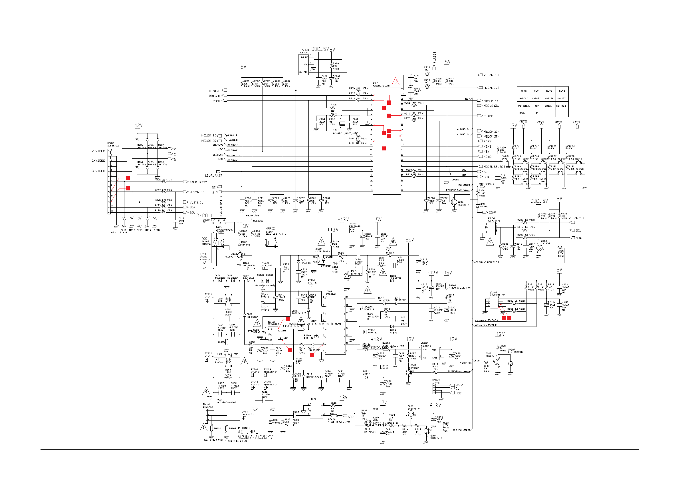
11 Schematic Diagrams
11-4 Micom/SMPS Part Schematic Diagram
4
8
9
13
12
10
11
7
5
1
3
2
14 15
11-2 CKA42*7L/5227L
 Loading...