

Page 1
Level
8.
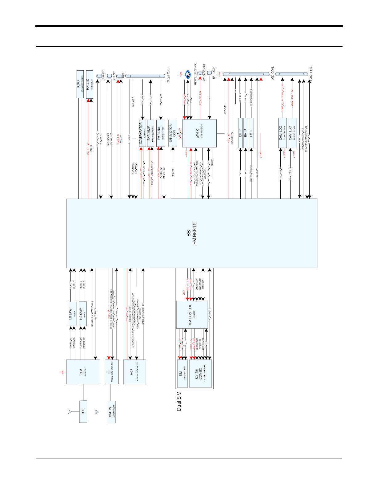
Block Diagram
8-1.
Repair
3
8-1
SAMSUNG Proprietary-Contents may change without notice
This Document can not be used without Samsung's authorization
Page 2
Level3Repair
PCB Diagrams
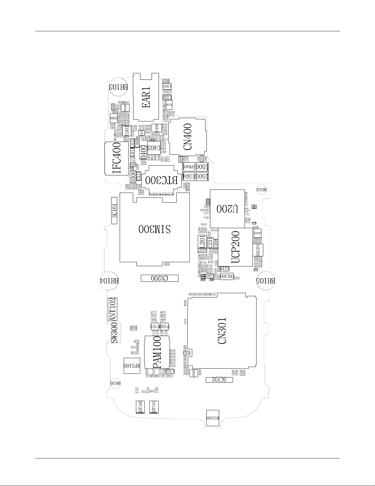
8-2.
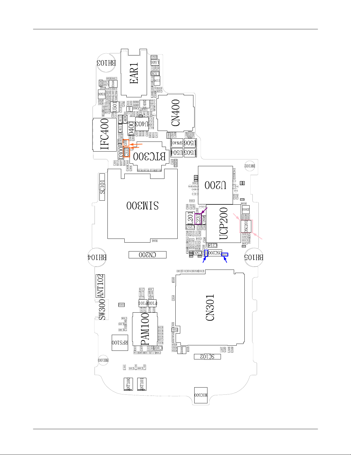
8-2-1.
Top
8-2
SAMSUNG Proprietary-Contents may change without notice
This Document can not be used without Samsung's authorization
Page 3
Level3Repair
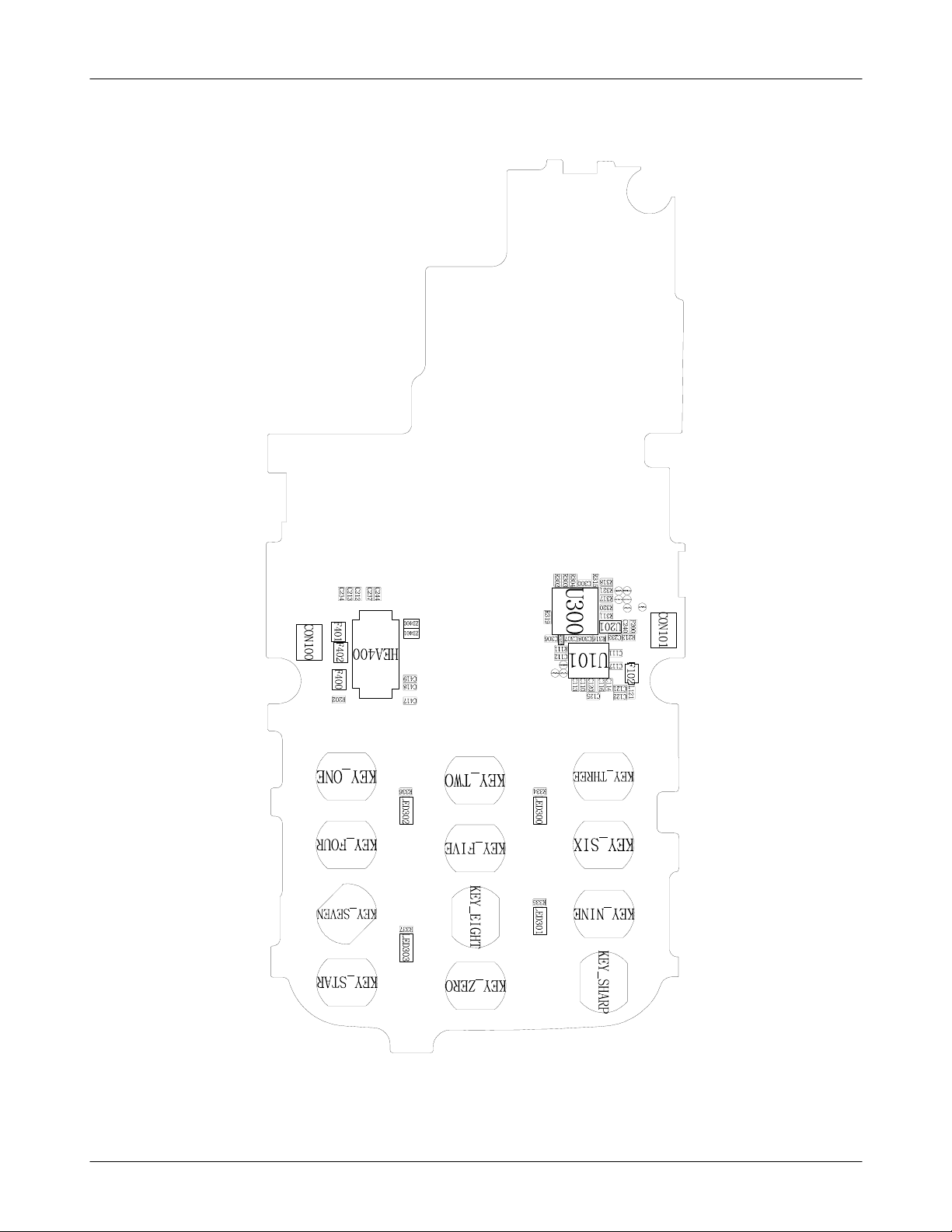
8-2-1.
Bottom
8-3
SAMSUNG Proprietary-Contents may change without notice
This Document can not be used without Samsung's authorization
Page 4
Level3Repair
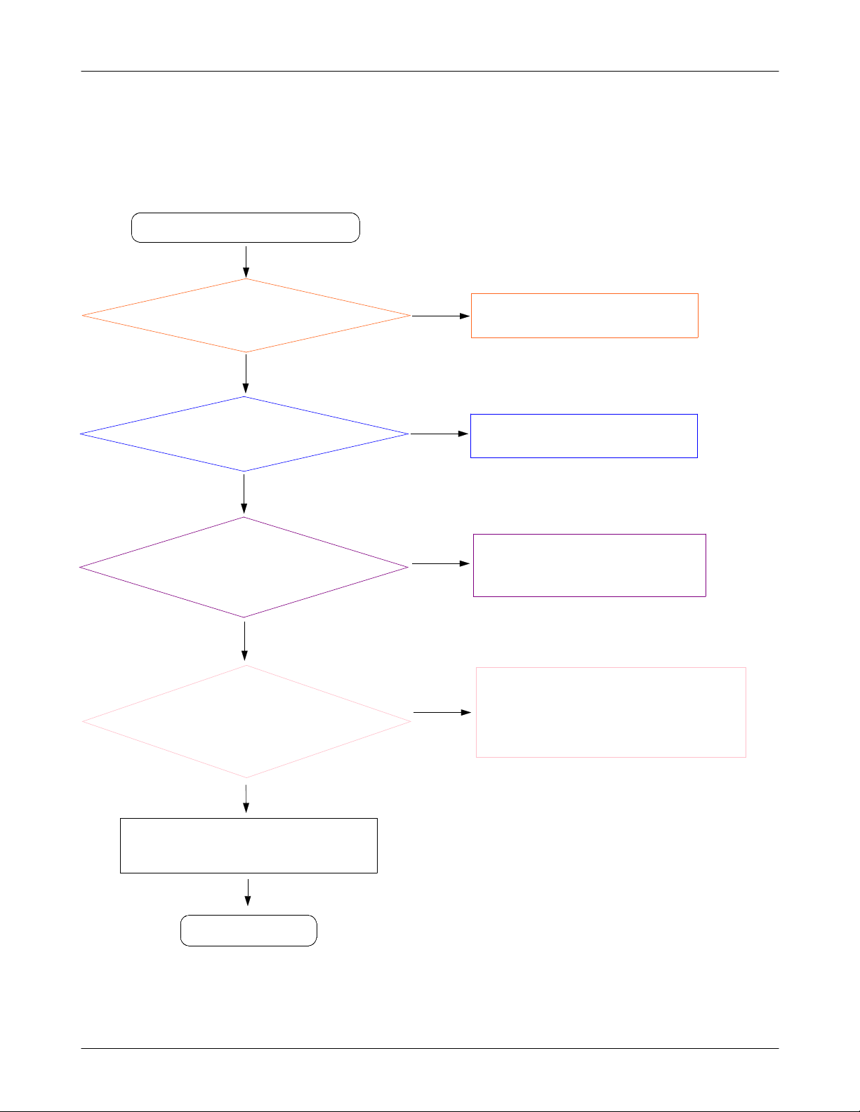
Flow Chart of Troubleshooting
8-3.
presetting methods for checking TP
※
GND&TP(exp. VBAT=
-
look over the coming out signal.
-
C105
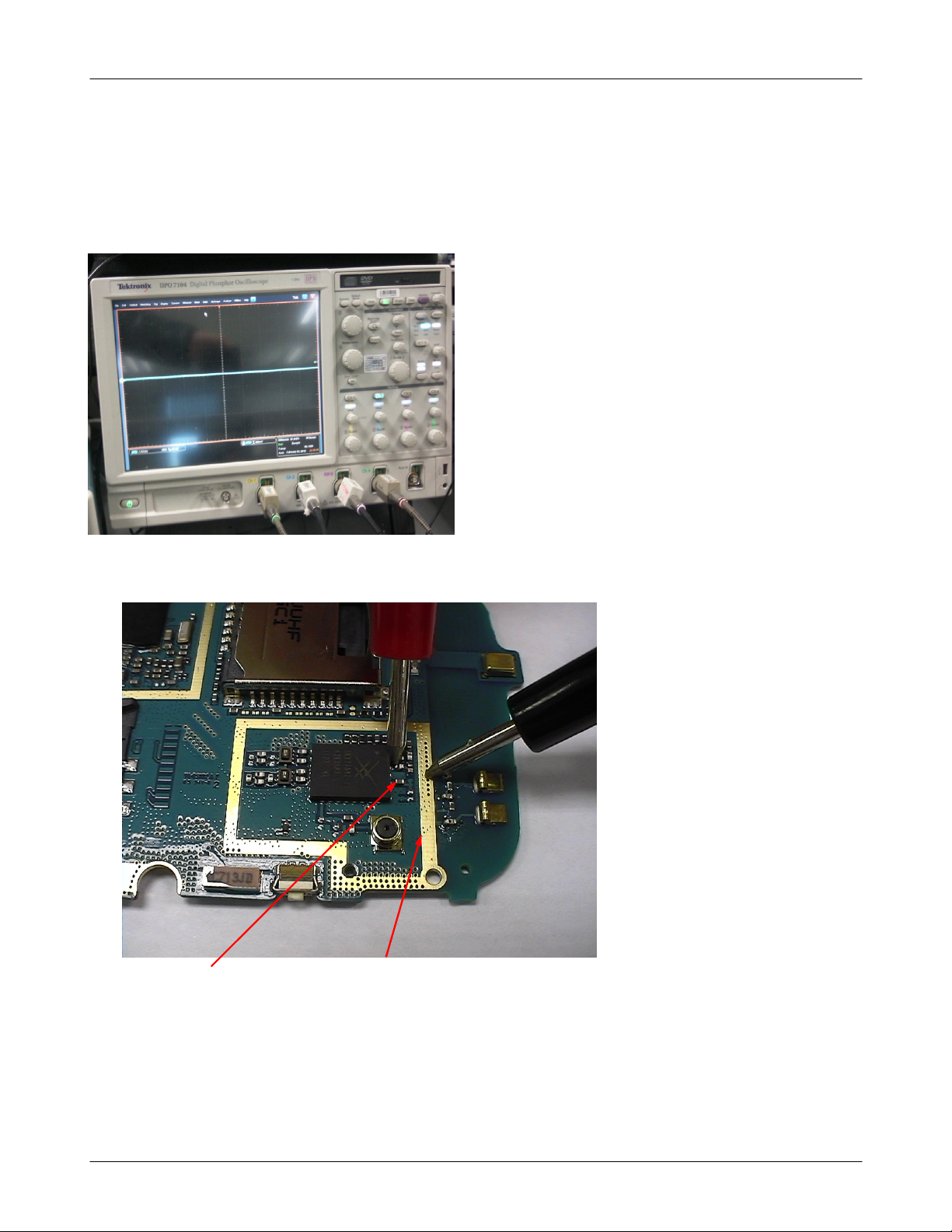
using Oscilloscope
)
Oscilloscope
←
TP(Test Point) GND
SAMSUNG Proprietary-Contents may change without notice
This Document can not be used without Samsung's authorization
8-4
Page 5
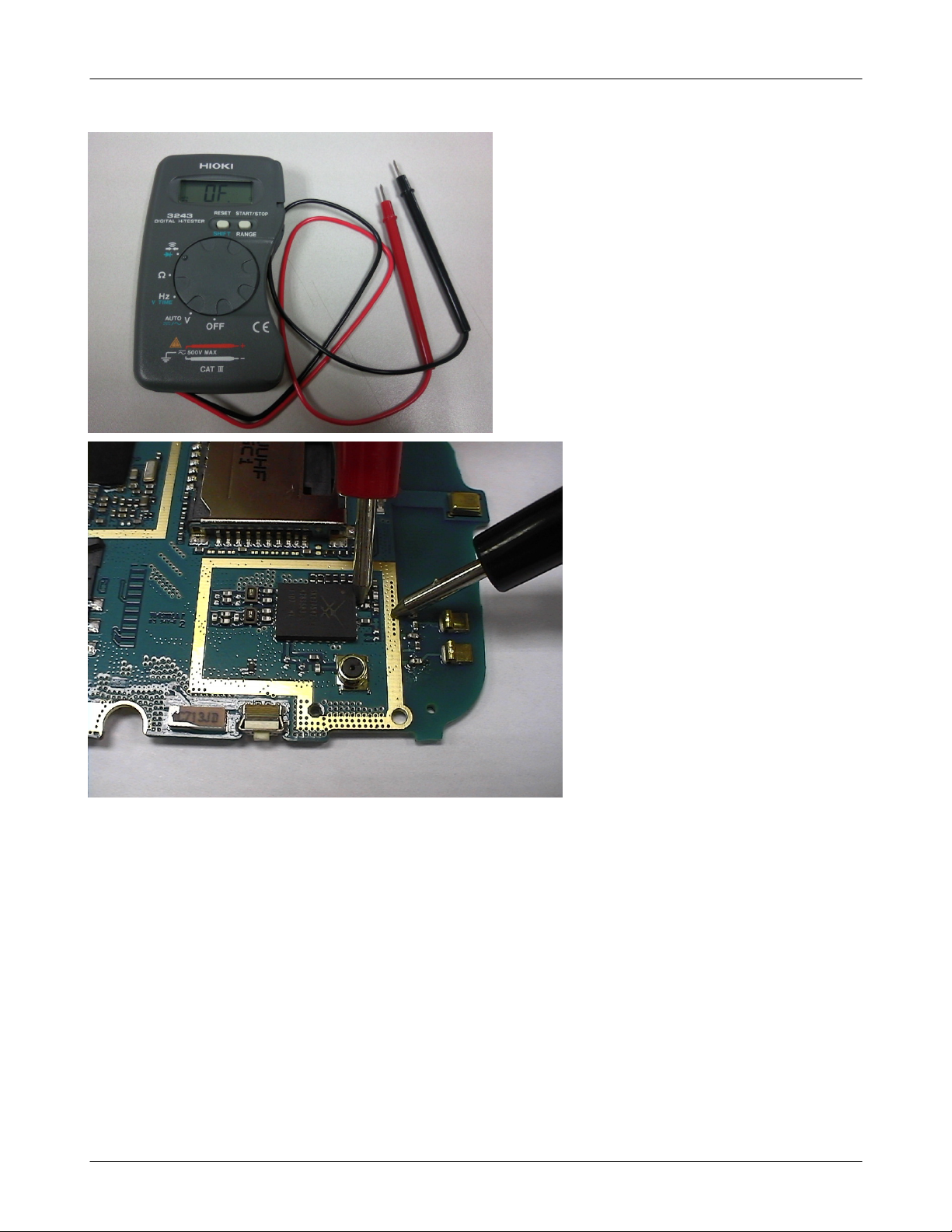
Multi-meter
←
Level3Repair
Checking the TP(test point) using Multi-meter
←
EX) to look up the TP, shunt Cap.
-
SAMSUNG Proprietary-Contents may change without notice
This Document can not be used without Samsung's authorization
-
if checking the GND, you can listen"beep"
if checking the Signal, you can't listen it.
8-5
Page 6
Level3Repair
8-3.
8-3-1.
LOGIC
Power On
Power On'does not work
'
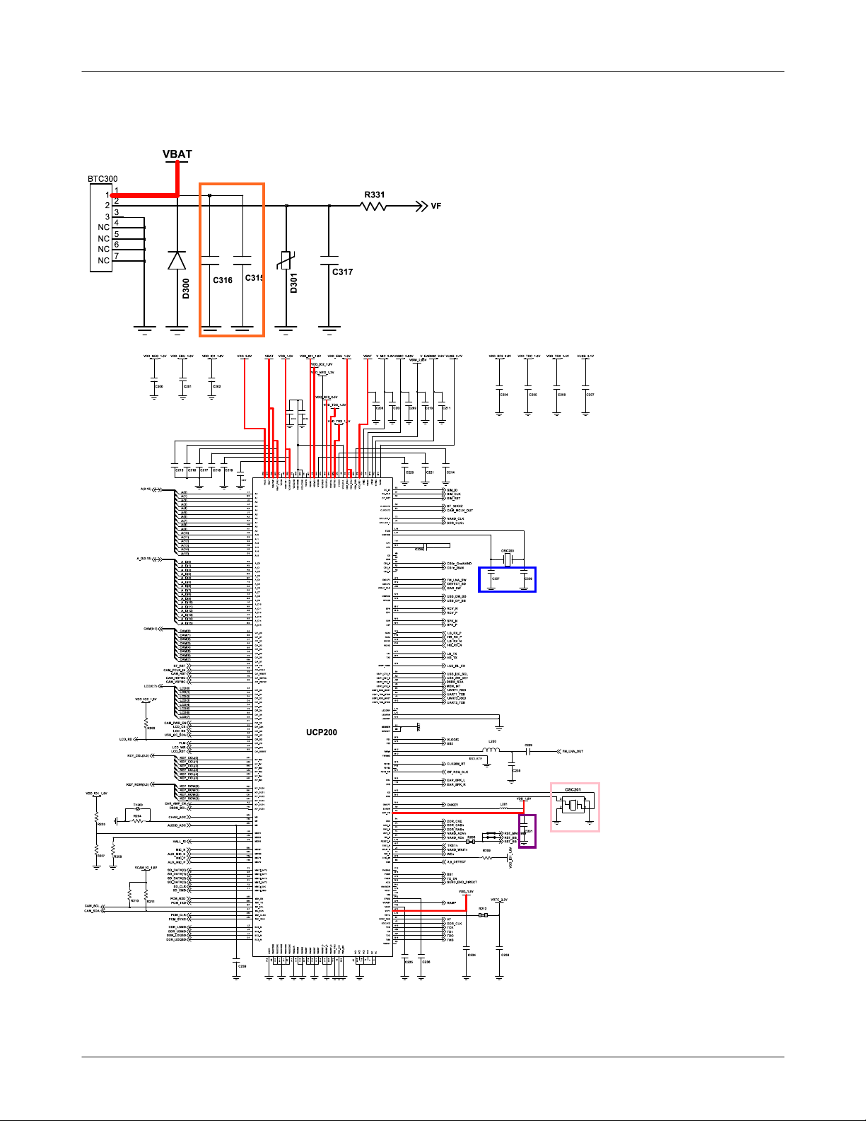
Check the Battery Voltage
is more than
Check the Clock at
OSC200(C227, C228,
32.768
Yes
TP:C315, C316)
(
kHz,
3.5V
Yes
±20
Yes
ppm)
No
Change the Battery
No
replace the OSC200
VDD_1.8V
TP: C231)
(
Check the Clock at
OSC201
when normal operating
(
condition,26MHz
Check the initial operation
END
=1.8
Yes
pin
1,3
±11
Yes
Yes
V?
ppm)
No
No
Check the Main Chip related to
SD1_FB=1.8V(TP:C231)
to lookover the Chip damage)
(
Check the Main Chip
to lookover the Chip damage)
(
(TP:
OSC201
pin/look over the waverform
1,3
using the oscilloscope)
8-6
SAMSUNG Proprietary-Contents may change without notice
This Document can not be used without Samsung's authorization
Page 7
Level3Repair
8-7
SAMSUNG Proprietary-Contents may change without notice
This Document can not be used without Samsung's authorization
Page 8
Level3Repair
8-8
SAMSUNG Proprietary-Contents may change without notice
This Document can not be used without Samsung's authorization
Page 9
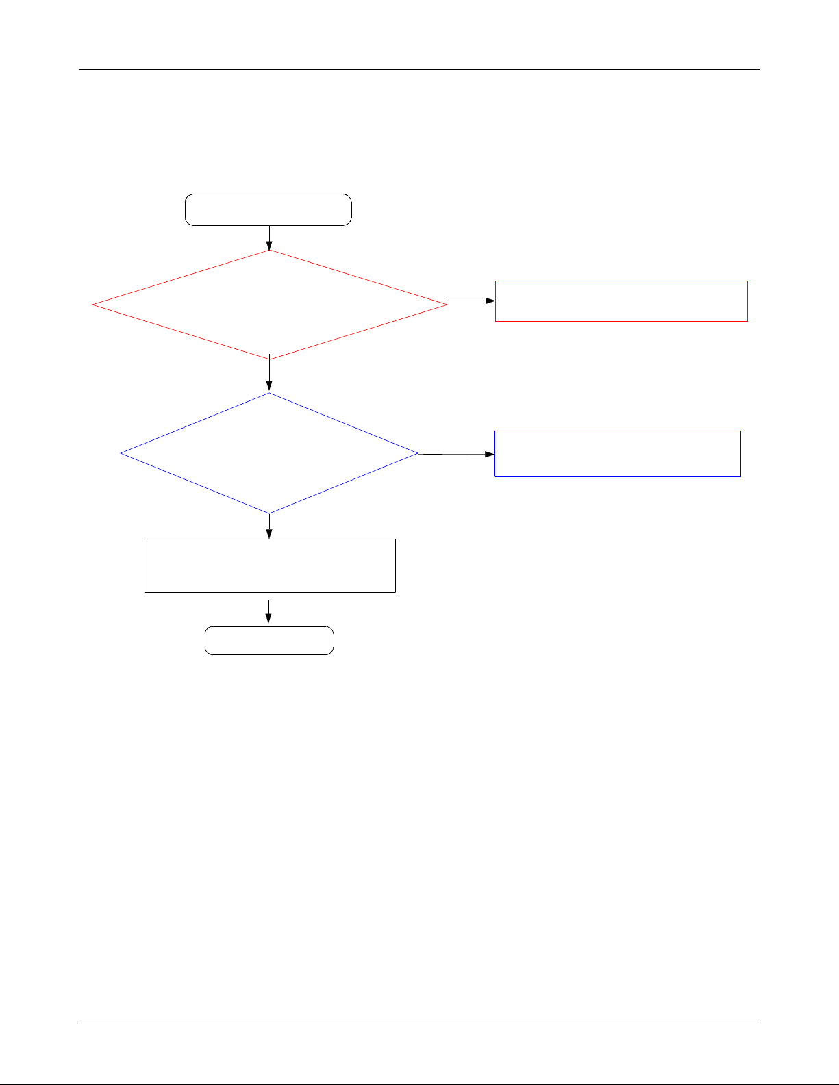
Level3Repair
8-3-2.
Initial
Initial Failure
Yes
R206(RST_BB
measure GND&SHORT PAD
,
using the oscilloscope
LCD_RST
(TP:
)>1.7V?
Yes
>1.7V?
HEA400 pin9)
Yes
.
No
Resolder R206, must be higher than
No
Change PBA.
1.7
V.
Check the16bit data signals.
Yes
END
8-9
SAMSUNG Proprietary-Contents may change without notice
This Document can not be used without Samsung's authorization
Page 10
Level3Repair
the5th pin from the the top of left pin.
8-10
SAMSUNG Proprietary-Contents may change without notice
This Document can not be used without Samsung's authorization
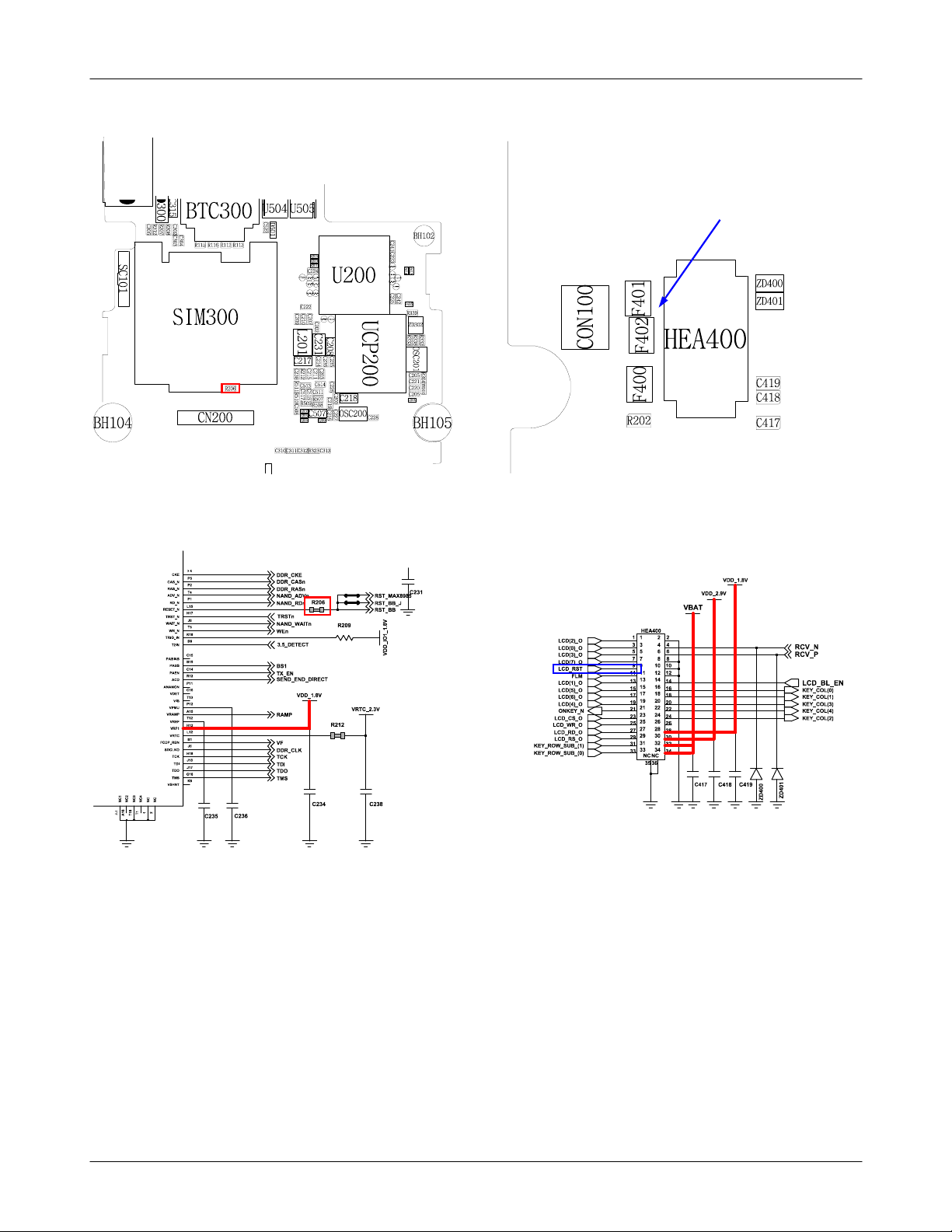
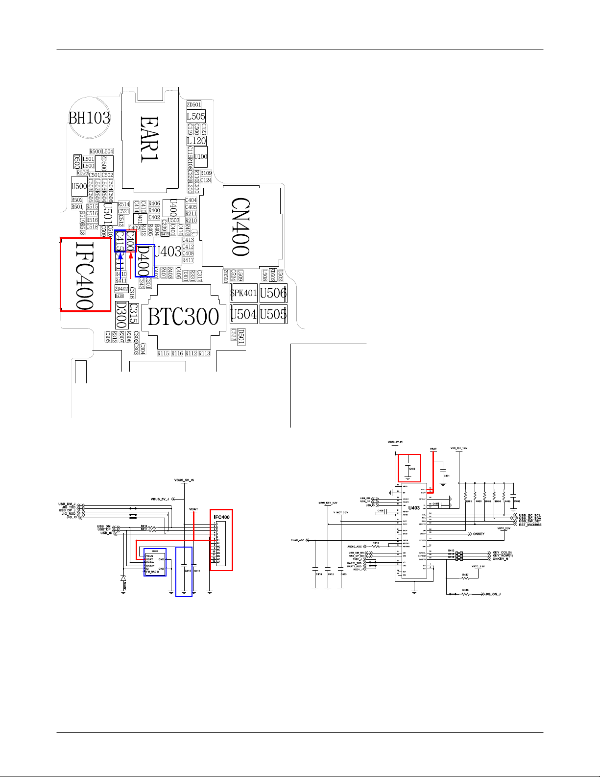
Page 11
Level3Repair
8-3-3.
Charging Part
Abnormal charging part
U403 pin E6(VBUS_5V_IN,
C400)
check the D400(short)
and C415, C400(short)
Yes
No
4.2V
≥
Yes
No
Yes
Resolder IFC400
Replace D400
or open the C415, C400
Check the Battery and TA
is connected correctly
Yes
END
8-11
SAMSUNG Proprietary-Contents may change without notice
This Document can not be used without Samsung's authorization
Page 12
Level3Repair
8-12
SAMSUNG Proprietary-Contents may change without notice
This Document can not be used without Samsung's authorization
Page 13
Level3Repair
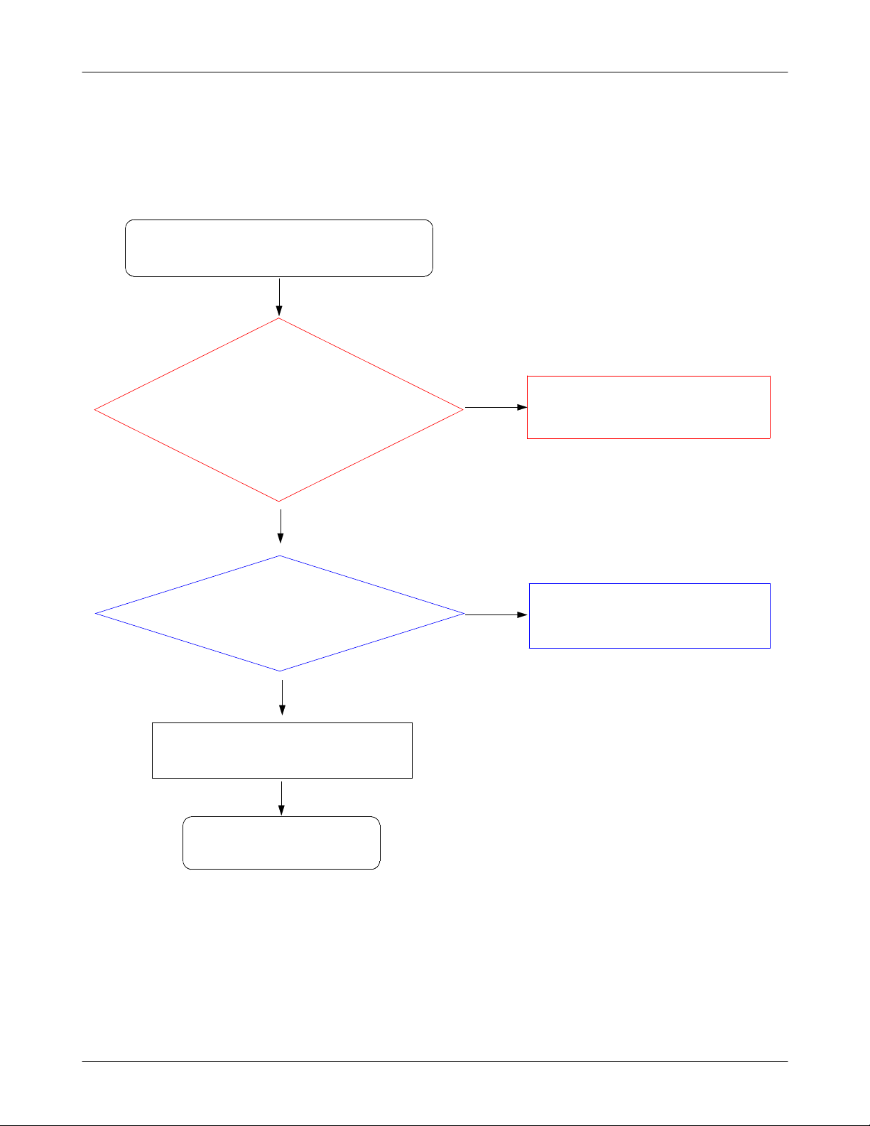
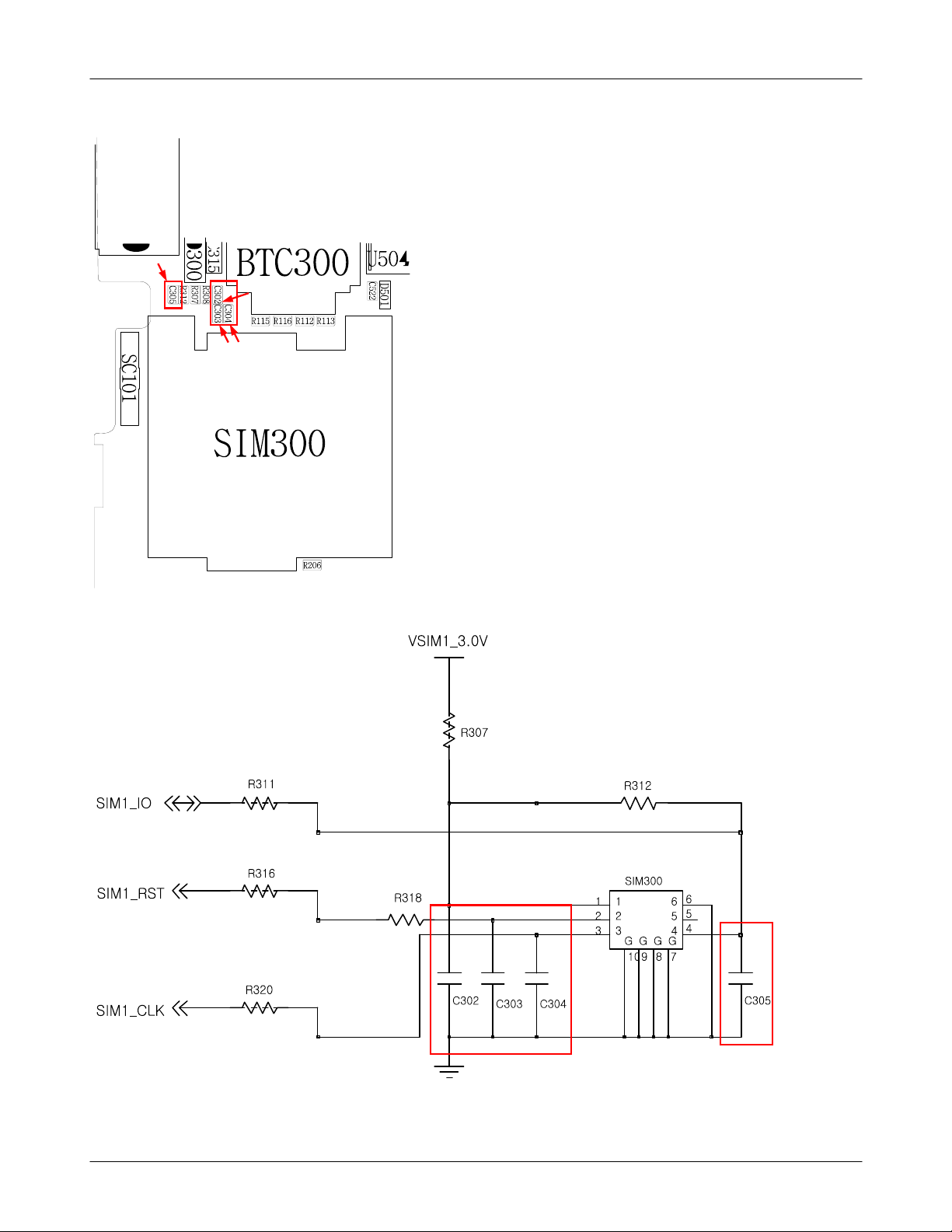
8-3-4.
Sim Part(SIM1)
Phone can't access SIM Card
SIM300 pin1(C302), pin4(C305)
3.0V?
≥
and
pin3(SIM_CLK)
Yes
≥
Yes
3
MHz
No
Resolder or Replace SIM300
?
Check signal sequence,
VSIM1_3.0V(C302)
SIM_IO(C305)→SIM_CLK(C304)
Check the SIM Card(is broken?)
SIM_RST(C303)
→
END
→
Yes
Yes
No
Change PBA
8-13
SAMSUNG Proprietary-Contents may change without notice
This Document can not be used without Samsung's authorization
Page 14
Level3Repair
8-14
SAMSUNG Proprietary-Contents may change without notice
This Document can not be used without Samsung's authorization
Page 15

Level3Repair
8-3-5.
Sim Part(SIM2)
Phone can't access SIM Card
CN301 pin
2.7V?
≥
and
pin15(SIM_CLK, C311)
11(
Yes
C313)
Yes
No
Resolder or Replace CN301
MHz
3
≥
?
Check signal sequence,
VSIM2_3.0V(C313)
SIM_IO(C312)→SIM_CLK(C311)
Check the SIM Card(is broken?)
SIM_RST(C310)
→
END
→
Yes
Yes
No
Change PBA
8-15
SAMSUNG Proprietary-Contents may change without notice
This Document can not be used without Samsung's authorization
Page 16

Level3Repair
8-16
SAMSUNG Proprietary-Contents may change without notice
This Document can not be used without Samsung's authorization
Page 17

Level3Repair
8-3-6.
Microphone Part
Microphone does not work
Yes
C203
=2.2V
at Mic Active?
Yes
Check the MIC Connection
look over schematics about
(
schemetics.)
No
No
Replace UCP200 usingaHeatgun
Because of not soldering well
(
Resolder L506, C513, C514, R511, L507, C519,
C520
not work if those are not connected.)
(
)
Yes
Check the MIC sample.
it be possible the problem
(
things)
Yes
END
No
Replace an another MIC
because of being possible the problem)
(
8-17
SAMSUNG Proprietary-Contents may change without notice
This Document can not be used without Samsung's authorization
Page 18

Level3Repair
8-18
SAMSUNG Proprietary-Contents may change without notice
This Document can not be used without Samsung's authorization
Page 19

Level3Repair
8-3-7.
Ear Microphone Part
Ear Microphone does not work
Yes
C211
at Ear Mic Active?
Check the Ear MIC Connection
look over schematics about
(
=2.2V
Yes
schemetics.)
Yes
No
No
Replace UCP200 usingaHeatgun
Because of not soldering well
(
Resolder L501, R507, R508, R509, C507, C508,
C511, C515, C517
not work if those is not connected.)
(
)
Check the Headset sample.
it be possible the problem
(
things)
Yes
END
No
Replace an another Headset
because of being possible the problem)
(
8-19
SAMSUNG Proprietary-Contents may change without notice
This Document can not be used without Samsung's authorization
Page 20

Level3Repair
8-20
SAMSUNG Proprietary-Contents may change without notice
This Document can not be used without Samsung's authorization
Page 21

Level3Repair
8-21
SAMSUNG Proprietary-Contents may change without notice
This Document can not be used without Samsung's authorization
Page 22

Level3Repair
8-3-8.
Speaker Part
Speaker does not work
Wiring the SPK N/P and
(
checking an waveform using
oscilloscope)
Does not work Voice call
Yes
L508, L509
>2.0V
Yes
Yes
No
be possible because of soldering not well)
(
?
No
be possible of being UCPabad sample)
(
Resolder L508&L509
Replace UCP200 usingaHeatgun
Does not work Ringtone?
Menu->Settings->Sound
(
profiles->Edit->
select the Call ringtone)
Yes
Is Speaker working?
Listening through the
(
speaker)
Yes
END
Resolder or Replace UCP200, U506, SPK401
No
No
be possible of soldering not well or being
(
UCPabad sample)
Change Speaker
be possible of SPK Problems
(
or not inserting it right.)
8-22
SAMSUNG Proprietary-Contents may change without notice
This Document can not be used without Samsung's authorization
Page 23

Level3Repair
8-23
SAMSUNG Proprietary-Contents may change without notice
This Document can not be used without Samsung's authorization
Page 24

Level3Repair
8-3-9.
Ear Speaker Part
Ear Speaker does not work
Yes
C509
at Ear Speaker active?
Does not work Voice call
Does not work Ringtone?
Menu->Settings->Sound
(
select the Call ringtone)
=1.8V
Yes
Yes
profiles->Edit->
No
No
?
No
Replace U501 usingaHeatgun
be possible of being U501abad sample)
(
Replace UCP200 usingaHeatgun
be possible of being UCPabad sample)
(
Resolder or Replace C509,C510,C512,
C516,C518,R514,R515,R516,C521,ZD500,L50
L503,C503,C504,R503,R504
2,
be possible of soldering not well or being
(
UCP, U501 are bad samples)
Yes
Is Ear Speaker working?
Listening through the
(
Ear speaker)
Yes
END
8-24
No
be possible of Ear SPK Problems)
(
Change Headset
SAMSUNG Proprietary-Contents may change without notice
This Document can not be used without Samsung's authorization
Page 25

Level3Repair
8-25
SAMSUNG Proprietary-Contents may change without notice
This Document can not be used without Samsung's authorization
Page 26

Level3Repair
8-26
SAMSUNG Proprietary-Contents may change without notice
This Document can not be used without Samsung's authorization
Page 27

Level3Repair
8-3-10.
Mo
Part
tor
otor does not work
M
C412
=3.3V
at Motor Active?
Check theMotor Connection
look over schematics about
(
schemetics.)
Yes
Yes
Yes
No
No
Replace U403 usingaHeatgun
Because of not soldering well
(
Resolder C522, D501, U504, U505
not work if those is not connected or
(
not soldering well.)
)
Check the Motor sample.
it be possible the problem
(
things)
Yes
END
No
Replace an another Speaker module sample
because of being possible the problem)
(
8-27
SAMSUNG Proprietary-Contents may change without notice
This Document can not be used without Samsung's authorization
Page 28

Level3Repair
8-28
SAMSUNG Proprietary-Contents may change without notice
This Document can not be used without Samsung's authorization
Page 29

Level3Repair
8-3-11.
Check Initial Operation
Key Data Input
Yes
Is it the
key or the SUB
Check the
adhesion condition,
(
foreign substances)
3×4
key?
3×4
3×4
domesheet
Key
key
SUB key
No
Check the SUB
key domesheet
condition, foreign
substances)
Change the
domesheet
or adhere correctly to
PBA.
3×4
key
adhesion
(
Yes
No
Change the SUB key
domesheet
or adhere correctly to
SUB PBA.
Yes
Check the key
circuit.
not connected, not
(
soldered, short)
Yes
END
No
resolder R332, R333,
R338, R339, ZD302,
D302
Check the
connection
condition.(not
connected slide
FPCB)
Check the SUB PBA
Yes
is broken?)
(
END
Yes
No
Reconnect slide
FPCB
8-29
SAMSUNG Proprietary-Contents may change without notice
This Document can not be used without Samsung's authorization
Page 30

Level3Repair
8-30
SAMSUNG Proprietary-Contents may change without notice
This Document can not be used without Samsung's authorization
Page 31

Level3Repair
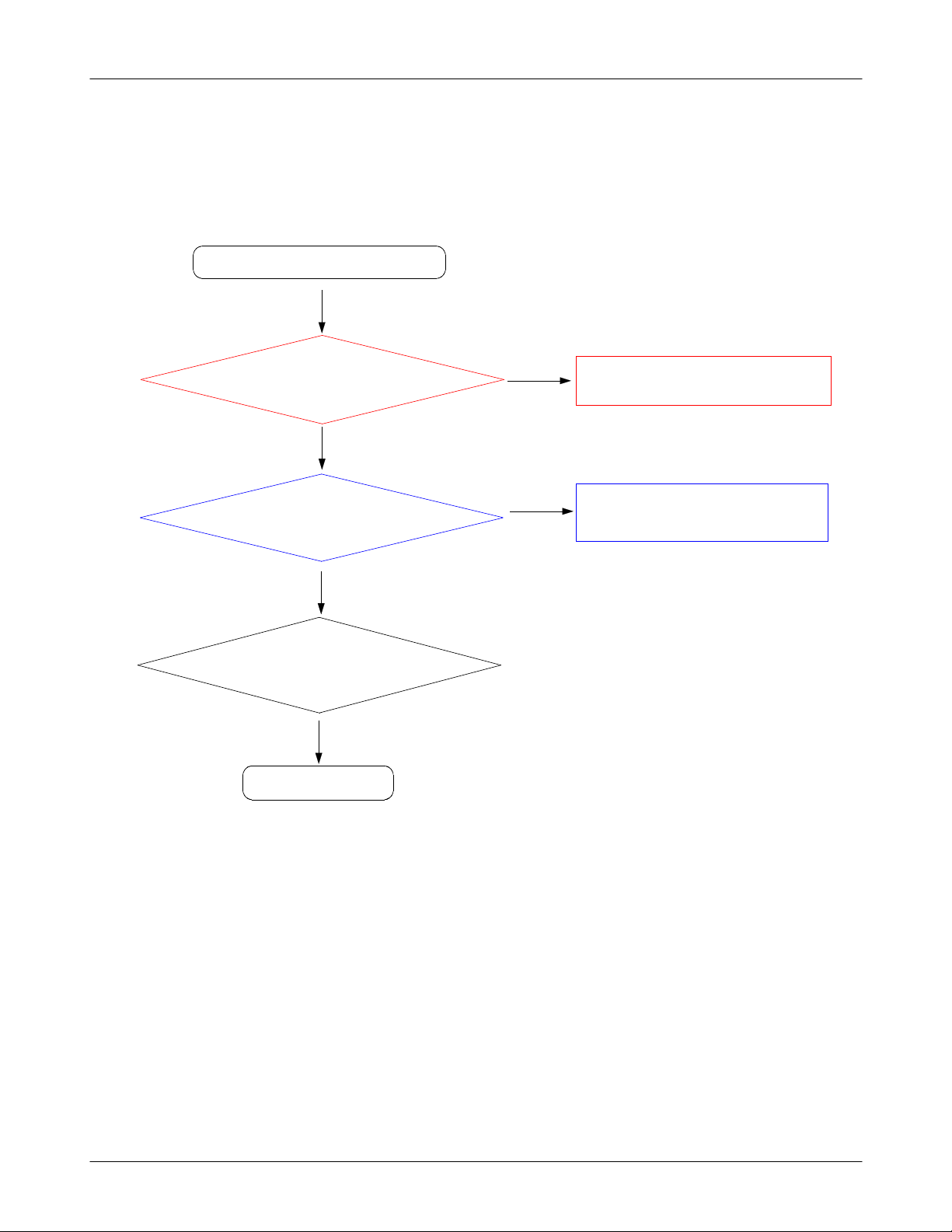
8-3-12.
Back Light(LCD)
LCD does not work
Yes
Check the LCD FPCB
connection, broken)
(
Yes
Check the slide FPCB
connection, broken)
(
Yes
No
No
Change the LCD module or connect the LCD
FPCB to SUB PBA correctly.
Change the SUB PBA or connect the slide
FPCB to PBA correctly.
The Voltage at C417=VBAT?
Yes
END
No
Check the HEA400 mounted to PBA correctly.
Resolder the C417.
8-31
SAMSUNG Proprietary-Contents may change without notice
This Document can not be used without Samsung's authorization
Page 32

Level3Repair
8-32
SAMSUNG Proprietary-Contents may change without notice
This Document can not be used without Samsung's authorization
Page 33

Level3Repair
8-3-13.
GSM
R100 using spectrum
(
F100
850 Rx
ON
Rx
Cell Power
PAM100
PAM100 Pin12
:-60
Yes
Pin
dBm
-65
analyzer)
Yes
dBm
-68
Yes
pin, L105,L108,
8,9
L107,L109
dBm
75
-
dBm
17
≥
≥
≥
No
No
Resolder PAM100,
check R100(open)
No
Check PAM100
control check
Yes
Resolder F100,L105,L106,L107,L108,L109
No
Check ANT Switch
control circuit
Resolder PAM100
Yes
Check UCP200 is working
Yes
END
8-33
SAMSUNG Proprietary-Contents may change without notice
This Document can not be used without Samsung's authorization
Page 34

Level3Repair
8-3-14.
GSM
R100 using spectrum
(
F100
900 Rx
RX ON
Cell Power
PAM100
PAM100 Pin11
:-60
Yes
Pin
dBm
-65
analyzer)
Yes
dBm
-68
Yes
pin, L105,L108,
8,9
L107,L109
dBm
75
-
17
dBm
≥
≥
≥
No
No
No
Resolder PAM100,
check R100(open)
Check PAM100
control check
Resolder F100,L104,L105,L107,L108,L109
No
Yes
Check ANT Switch
control circuit
Resolder PAM100
Yes
Check UCP200is working
Yes
END
8-34
SAMSUNG Proprietary-Contents may change without notice
This Document can not be used without Samsung's authorization
Page 35

Level3Repair
8-3-15.
DCS
Cell Power
PAM100
R100 using spectrum
(
F101
L119, L117, L118
Rx
RX ON
:-60
Yes
Pin
17
dBm
-65
analyzer)
Yes
PAM100 Pin14
dBm
-68
Yes
pin, L113,
9,8
dBm
-75
dBm
≥
≥
No
No
≥
No
Resolder PAM100,
check R100(open)
Check PAM100
control check
Resolder F101,L113,L116,L117,L118,L119
No
Yes
Check ANT Switch
control circuit
Resolder PAM100
Yes
Check UCP200is working
Yes
END
8-35
SAMSUNG Proprietary-Contents may change without notice
This Document can not be used without Samsung's authorization
Page 36

Level3Repair
8-3-16.
PCS
Cell Power
PAM100
R100 using spectrum
(
F101
L119, L117, L118
Rx
RX ON
:-60
Yes
Pin
17
dBm
-65
analyzer)
Yes
PAM100 Pin13
dBm
-68
pin, L113,
9,8
dBm
-75
Yes
dBm
≥
≥
No
No
≥
No
Resolder PAM100,
check R100(open)
Check PAM100
control check
Resolder F101,L113,L115,L117,L118,L119
No
Yes
Check ANT Switch
control circuit
Resolder PAM100
Yes
Check UCP200is working
Yes
END
8-36
SAMSUNG Proprietary-Contents may change without notice
This Document can not be used without Samsung's authorization
Page 37

Level3Repair
8-37
SAMSUNG Proprietary-Contents may change without notice
This Document can not be used without Samsung's authorization
Page 38

Level3Repair
8-38
SAMSUNG Proprietary-Contents may change without notice
This Document can not be used without Samsung's authorization
Page 39

Level3Repair
8-3-17.
GSM
850/900 Tx
TX Power is too Low!!
TX ON(5Level)
CLOCK CHECK?
MHz@OSC201(pin1,
26
PAM100 pin
R106 using spectrum
(
Check the Voltage
analyzer)
C103
pin3)
dBm
〉
YES
27≥-1
YES
V?
3.3
NO
NO
NO
solder OSC200
Re-
solder or change
Re-
UCP200
Check the UCP200&VBAT
circuit.
YES
PAM100
R100 using spectrum
(
Check the RFS100
connection with PCB?
re-solder or change
Pin
dBm
30
analyzer)
YES
YES
Antenna
17
≥
NO
NO
Resolder PAM100
Resolder RFS100.
8-39
SAMSUNG Proprietary-Contents may change without notice
This Document can not be used without Samsung's authorization
Page 40

Level3Repair
8-3-18.
DCS/PCS
Tx
TX Power is too Low!!
TX ON(5Level)
CLOCK CHECK?
MHz@OSC201(pin1,
26
PAM100 pin
(
pin3)
dBm
L111 using spectrum
analyzer)
Check the Voltage
C103
〉
YES
29≥-1
YES
V?
3.3
YES
NO
NO
NO
solder OSC200
Re-
solder or change
Re-
UCP200
Check the UCP200&VBAT
circuit.
PAM100
R100 using spectrum
(
Check the RFS100
connection with PCB?
re-solder or change
Pin
dBm
30
analyzer)
YES
YES
Antenna
17
≥
NO
Resolder PAM100
NO
Resolder RFS100.
8-40
SAMSUNG Proprietary-Contents may change without notice
This Document can not be used without Samsung's authorization
Page 41

Level3Repair
8-41
SAMSUNG Proprietary-Contents may change without notice
This Document can not be used without Samsung's authorization
Page 42

Level3Repair
8-42
SAMSUNG Proprietary-Contents may change without notice
This Document can not be used without Samsung's authorization
Page 43

NC Point(Top View)
-
NC
:
U101
123456
A
○○○○○○
B
○○○●○●
C
○○○○●●
D
○○○○○○
E
○○●●●○
Level3Repair
UCP200
123456789101112131415161718
A
○○○○○○○○○○○○○○○○○●
B
○○○○○○○○○○○○○○○○○○
C
○○○○○○○○○○○○○○●●○○
D
○○○○○○○○○○○○○○○○○○
E
○○○○○○○○○○○○○○○○○○
F
○○○○○○○○○○●○●○○○○○
G
○○○○○○○○○○○○○○○○○○
H
○○○○○○○○○○○○○○○○○○
J
○○○○○○○○○○○○○○○○○○
K
○○○○○○○●○○○○○○○○○○
L
○○○○○○○○○○●○○○○○○○
M
○○○○○○○○●○○○○○○○○○
N
○○○○○○○○○○○○○○○○○○
P
○○○○○○○○○○●○○○○○○○
R
○○○○○●○●○○○○○○○○○○
T
●○○○○●●○○●○○○○○○○○
8-43
SAMSUNG Proprietary-Contents may change without notice
This Document can not be used without Samsung's authorization
Page 44

Level3Repair
U200
1234567891011121314
A
●●○○○○○○○○○○●●
B
●○○○○○○○○○○○○●
C
○○○○○○○○○○○○○○
D
○○○●○○○○○○○○○○
E
○○○○○○○○○○○○○○
F
○○○○○○○○○○○○○○
G
○○○○○○○○○○○○○○
H
○○○○○○○○○○○○○○
J
○○○○○○○○○○○○○○
K
○○○○○○○○○○○○○○
L
○○○○○○○○○○○○○○
M
○○○○○○○○○○○○○○
N
●○○○○○○○○○○○○●
P
●●○○○○○○○○○○●●
8-44
SAMSUNG Proprietary-Contents may change without notice
This Document can not be used without Samsung's authorization
Page 45

U403
123456
A
●○○○○○
B
●●○○○○
C
○○○○○○
D
○○○○○○
E
○○○○○○
F
○○○○●●
Level3Repair
8-45
SAMSUNG Proprietary-Contents may change without notice
This Document can not be used without Samsung's authorization
 Loading...