

Page 1
Page 2
Page 3
Page 4
General Description Product Summary
V
A
C
C
A
AOD4184A
40V N-Channel MOSFET
The AOD4184A combines advanced trench MOSFET
technology with a low resistance package to provide
extremely low R
. This device is well suited for high
DS(ON)
current load applications.
DS
ID (at VGS=10V)
R
R
(at VGS=10V)
DS(ON)
(at VGS = 4.5V)
DS(ON)
40V
50A
< 7mΩ
< 9.5mΩ
100% UIS Tested
100% Rg Tested
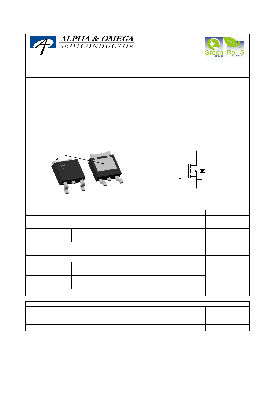
TO252
DPAK
Top View
D
G
Absolute Maximum Ratings T
A
Drain-Source Voltage 40
Continuous Drain
Current
G
Pulsed Drain Current
Continuous Drain
Current
TC=25°C
=100°C
T
C
C
=25°C
T
A
T
=70°C
A
Avalanche Current
Avalanche energy L=0.1mH
=25°C
T
C
Power Dissipation
Power Dissipation
B
=100°C
C
T
=25°C
A
A
T
=70°C
A
Junction and Storage Temperature Range -55 to 175 °C
Bottom View
D
S
G
S
=25°C unless otherwise noted
Symbol
V
DS
V
GS
I
D
I
DM
I
DSM
IAS, I
AR
EAS, E
AR
P
D
P
DSM
TJ, T
STG
G
Maximum UnitsParameter
50
40
120
13
10
61
50
25T
2.3
1.5
D
S
mJ
W
W
V
V±20Gate-Source Voltage
A
A
A35
Thermal Characteristics
Parameter Typ Max
Maximum Junction-to-Ambient
Maximum Junction-to-Case
D
t ≤ 10s
Steady-State
Steady-State
Symbol
R
θJA
R
θJC
18
44
2.4
22
55
3
Units
°C/W
°C/WMaximum Junction-to-Ambient
°C/W
Rev0 : Sep 2009 www.aosmd.com Page 1 of 6
Page 5
Symbol
Symbol
Typ
Max
Absolute Maximum Ratings T
=25°C unless otherwise noted
C
C
C
A,G
A,G
AOD4189
TO-252
Top View
P-Channel Enhancement Mode Field Effect Transistor
General Description
The AOD4189 uses advanced trench technology and
design to provide excellent R
charge. With the excellent thermal resistance of the
DPAK package, this device is well suited for high
current load applications.
-RoHS Compliant
-Halogen Free*
D-PAK
D
G
Drain-Source Voltage
T
Continuous Drain
Current
B,H
=25°C
C
T
=100°C
C
Pulsed Drain Current
Avalanche Current
Repetitive avalanche energy L=0.1mH
TC=25°C
B
A
TC=100°C
=25°C
T
A
TA=70°C
Power Dissipation
Power Dissipation
Junction and Storage Temperature Range
with low gate
DS(ON)
Bottom View
S
C
S
G
V
DS
V
GS
I
D
I
DM
I
AR
E
AR
P
D
P
DSM
TJ, T
STG
Features
VDS (V) = -40V
I
= -40A (VGS = -10V)
D
R
R
100% UIS Tested!
100% Rg Tested!
< 22mΩ (VGS = -10V)
DS(ON)
< 29mΩ (VGS = -4.5V)
DS(ON)
G
Maximum UnitsParameter
-40
-40
-28
-50
-35
61
62.5
31
2.5
1.6
-55 to 175
D
S
V
V±20Gate-Source Voltage
A
mJ
W
°C
Thermal Characteristics
Parameter Units
Maximum Junction-to-Ambient
Maximum Junction-to-Ambient
Maximum Junction-to-Case
Alpha & Omega Semiconductor, Ltd.
D,F
t ≤ 10s
Steady-State
Steady-State
R
θJA
R
θJC
15 20
41 50
2 2.4
°C/W
°C/W
°C/W
www.aosmd.com
Page 6

AOD4189
Electrical Characteristics (T
Symbol Min Typ Max Units
=25°C unless otherwise noted)
J
Parameter Conditions
STATIC PARAMETERS
I
BV
I
DSS
I
GSS
V
GS(th)
I
D(ON)
R
DS(ON)
g
FS
V
SD
I
S
DSS
Drain-Source Breakdown Voltage
Zero Gate Voltage Drain Current
Gate-Body leakage current
Gate Threshold Voltage
On state drain current
Static Drain-Source On-Resistance
Forward Transconductance
Diode Forward Voltage
Maximum Body-Diode Continuous Current
=-250µA, VGS=0V
D
V
=-40V, VGS=0V
DS
V
=0V, VGS= ±20V
DS
V
DS=VGS ID
=-250µA
VGS=-10V, VDS=-5V
VGS=-10V, ID=-12A
=-4.5V, ID=-8A
V
GS
=-5V, ID=-12A
V
DS
=-1A,VGS=0V
I
S
-40 V
=55°C -5
T
J
-1.7 -1.9 -3 V
-50 A
18 22
=125°C 27 33
T
J
23 29
35 S
-0.74 -1 V
-1
±100
-20 A
µA
nA
mΩ
DYNAMIC PARAMETERS
C
iss
C
oss
C
rss
R
g
Input Capacitance
Output Capacitance
Reverse Transfer Capacitance
Gate resistance
VGS=0V, VDS=-20V, f=1MHz
=0V, VDS=0V, f=1MHz
V
GS
2.5 4.5 6.5 Ω
1870 pF
185 pF
155 pF
SWITCHING PARAMETERS
(-10V) 31.4 41 nC
Q
g
Q
(-4.5V) 7.9 10
g
Q
gs
Q
gd
t
D(on)
t
r
t
D(off)
t
f
t
rr
Q
rr
A: The value of R
based on T
B. The power dissipation P
dissipation limit for cases where additional heatsinking is used.
C: Repetitive rating, pulse width limited by junction temperature T
D. The R
E. The static characteristics in Figures 1 to 6 are obtained using t ≤300 µs pulses, duty cycle 0.5% max.
F. These curves are based on the junction-to-case thermal impedence which is measured with the device mounted to a large heatsink, assuming
a maximum junction temperature of T
G. These tests are performed with the device mounted on 1 in
H. The maximum current rating is limited by bond-wires.
*This device is guaranteed green after data code 8X11 (Sep 1ST 2008).
Rev1: Oct 2008
COMPONENTS IN LIFE SUPPORT DEVICES OR SYSTEMS ARE NOT AUTHORIZED. AOS DOES NOT ASSUME ANY LIABILITY ARISING
OUT OF SUCH APPLICATIONS OR USES OF ITS PRODUCTS. AOS RESERVES THE RIGHT TO IMPROVE PRODUCT DESIGN,
FUNCTIONS AND RELIABILITY WITHOUT NOTICE.
Total Gate Charge
Total Gate Charge
Gate Source Charge
V
GS
I
D
Gate Drain Charge
Turn-On DelayTime
Turn-On Rise Time
Turn-Off DelayTime
V
GS
R
GEN
Turn-Off Fall Time
=-12A, dI/dt=100A/µs
Body Diode Reverse Recovery Time
Body Diode Reverse Recovery Charge
is measured with the device in a still air environment with TA =25°C. The power dissipation P
θJA
=150°C, using steady state junction-to-ambient thermal resistance.
J(MAX)
is the sum of the thermal impedence from junction to case R
θJA
is based on T
D
J(MAX)
=175°C, using junction-to-case thermal resistance, and is more useful in setting the upper
J(MAX)
=175°C. The SOA curve provides a single pulse rating.
I
F
=-12A, dI/dt=100A/µs
I
F
J(MAX)
2
FR-4 board with 2oz. Copper, in a still air environment with TA=25°C.
=-10V, VDS=-20V,
=-12A
=-10V, VDS=-20V, RL=1.6Ω,
=3Ω
=175°C.
and case to ambient.
θJC
TBD
TBD
7.6 nC
6.2 nC
10 ns
18 ns
38 ns
24 ns
32 42
30 nC
and current rating I
DSM
DSM
ns
are
Alpha & Omega Semiconductor, Ltd.
www.aosmd.com
Page 7

AOD4189
TYPICAL ELECTRICAL AND THERMAL CHARACTERISTICS
-4.0V
-6.0V
25°C
125°C
ID=-12A
D
VGS=-4.5V
VGS=-10V
25°C
125°C
50
-10V
-4.5V
40
30
(A)
D
-I
20
VGS=-3.5V
10
0
0 1 2 3 4 5
-VDS (Volts)
Figure 1: On-Region Characteristics
30
28
26
)
Ω
Ω
Ω
Ω
24
(m
22
DS(ON)
R
20
50
VDS=-5V
40
30
(A)
D
-I
20
10
125°C
25°C
0
1.5 2 2.5 3 3.5 4 4.5
-V
(Volts)
GS
Figure 2: Transfer Characteristics
2
1.8
VGS=-10V
1.6
VGS=-4.5V
I
1.4
=-8A
1.2
18
16
0 10 20 30 40
-I
(A)
D
Figure 3: On-Resistance vs. Drain Current and
Gate Voltage
55
50
45
)
40
Ω
Ω
Ω
Ω
(m
35
DS(ON)
30
R
25
20
15
3 4 5 6 7 8 9 10
-V
(Volts)
GS
Figure 5: On-Resistance vs. Gate-Source Voltage
ID=-12A
1
Normalized On-Resistance
0.8
-50 -25 0 25 50 75 100 125 150 175 200
Temperature (°C)
Figure 4: On-Resistance vs. Junction
Temperature
100
150
10
1
0.1
(A)
S
-I
0.01
0.001
0.0001
0.00001
0.0 0.2 0.4 0.6 0.8 1.0 1.2
(Volts)
-V
SD
Figure 6: Body-Diode Characteristics
mJ
Alpha & Omega Semiconductor, Ltd.
www.aosmd.com
Page 8

AOD4189
TYPICAL ELECTRICAL AND THERMAL CHARACTERISTICS
C
rss
limited
TC=25°C
TonT
D=0.5, 0.3, 0.1, 0.05, 0.02, 0.01, single pulse
10
VDS=-20V
I
=-12A
D
8
6
(Volts)
GS
4
-V
2
0
0 5 10 15 20 25 30 35
(nC)
Q
g
Figure 7: Gate-Charge Characteristics
100
10
R
(Amps)
D
-I
DS(ON)
2800
2400
C
iss
2000
1600
1200
Capacitance (pF)
800
C
400
oss
0
0 5 10 15 20 25 30 35 40
-VDS (Volts)
Figure 8: Capacitance Characteristics
10000
1000
Power (W)
100
T
T
J(Max)
=25°C
C
=175°C
T
=175°C
J(Max)
DC
1
1 10 100
(Volts)
-V
DS
Figure 9: Maximum Forward Biased
Safe Operating Area (Note F)
10
D=Ton/T
T
J,PK=Tc+PDM.ZθJC.RθJC
R
=2.4°C/W
θJC
In descending order
10
0.00001 0.0001 0.001 0.01 0.1 1
Pulse Width (s)
Figure 10: Single Pulse Power Rating Junction-to-
Case (Note F)
150
1
0.1
Normalized Transient
Thermal Resistance
Jc
θ
θ
θ
θ
Z
P
D
Single Pulse
0.01
0.00001 0.0001 0.001 0.01 0.1 1
Pulse Width (s)
Figure 11: Normalized Maximum Transient Thermal Impedance (Note F)
mJ
Alpha & Omega Semiconductor, Ltd.
www.aosmd.com
Page 9

AOD4189
T
on
T
D=0.5, 0.3, 0.1, 0.05, 0.02, 0.01, single pulse
TYPICAL ELECTRICAL AND THERMAL CHARACTERISTICS
100
10
, Peak Avalanche Current (A)
A
-I
1
0.01 0.1 1 10 100 1000
Time in Avalache, tA (s)
Figure 12: Single Pulse Avalanche Capability
50
40
(A)
D
30
20
Current rating -I
10
70
60
50
40
30
20
Power Dissipation (W)
10
0
0 25 50 75 100 125 150 175
(°C)
T
Figure 13: Power De-rating (Note B)
CASE
10000
T
J(Max)
T
=25°C
A
1000
100
Power (W)
10
=150°C
0
0 25 50 75 100 125 150 175
T
(°C)
CASE
Figure 14: Current De-rating (Note B)
1
1E-04 0.001 0.01 0.1 1 10 100 1000
Pulse Width (s)
Figure 15: Single Pulse Power Rating Junction-
to-Ambient (Note G)
10
D=Ton/T
T
J,PK=TA+PDM.ZθJA.RθJA
R
=50°C/W
θJA
1
In descending order
150
0.1
P
Normalized Transient
Thermal Resistance
0.01
JA
θ
θ
θ
θ
Z
D
Single Pulse
0.001
0.00001 0.0001 0.001 0.01 0.1 1 10 100 1000
Pulse Width (s)
Figure 16: Normalized Maximum Transient Thermal Impedance (Note G)
Alpha & Omega Semiconductor, Ltd.
www.aosmd.com
Page 10

AOD4189
VDC
Rg
Gate Charge Test Circuit & W aveform
Vgs
Qg
-
-
+
VDC
Vds
+
-10V
Qgs Qgd
DUT
Vgs
Ig
Charge
Resistive Switching Test Circuit & Waveforms
RL
Vds
Vgs
t
d(on)
t
on
t
r
t
off
t
t
d(off)
f
-
Vgs
DUT
VDC
Vdd
+
90%
Vgs
Vgs
Vds +
Vds -
Ig
Rg
Vgs
Isd
Vgs
Vds
Id
Vds
Unclamped Induc tive Switching (U IS) Test Circuit & Waveforms
L
DUT
Vgs
VDC
-
Vdd
+
E = 1/2 LI
AR
Vds
Id
Vgs
2
AR
Diode Recovery Test Circuit & Waveforms
Q = - Idt
rr
DUT
L
+
Vdd
VDC
-
Vgs
-Isd
-Vds
-I
F
dI/dt
10%
BV
DSS
I
AR
t
rr
-I
RM
Vdd
Alpha & Omega Semiconductor, Ltd. www.aosmd.com
Page 11

Ω
A
AOD4184A
Electrical Characteristics (T
Symbol Min Typ Max Units
=25°C unless otherwise noted)
J
Parameter Conditions
STATIC PARAMETERS
BV
I
DSS
I
GSS
V
GS(th)
I
D(ON)
R
DS(ON)
g
FS
V
SD
I
S
DSS
Drain-Source Breakdown Voltage
Zero Gate Voltage Drain Current
Gate-Body leakage current
Gate Threshold Voltage
On state drain current
Static Drain-Source On-Resistance
Forward Transconductance
Diode Forward Voltage
Maximum Body-Diode Continuous Current
I
=250µA, VGS=0V
D
V
=40V, VGS=0V
DS
=0V, VGS= ±20V
V
DS
V
DS=VGS ID
V
GS
V
GS
V
GS
V
DS
=1A,VGS=0V
I
S
=250µA
=10V, VDS=5V
=10V, ID=20A
=4.5V, ID=15A
=5V, ID=5A
T
=55°C
J
=125°C
T
J
40 V
1
µA
5
±100 nA
1.7 2.1 2.6 V
120 A
5.8 7
9.6 12
7.6 9.5
mΩ
m
37 S
0.7 1 V
20 A
DYNAMIC PARAMETERS
C
iss
C
oss
C
rss
R
g
Input Capacitance
Output Capacitance
Reverse Transfer Capacitance
Gate resistance V
V
=0V, VDS=20V, f=1MHz
GS
=0V, VDS=0V, f=1MHz
GS
1200 1500 1800 pF
150 215 280 pF
80 135 190 pF
2 3.5 5 Ω
SWITCHING PARAMETERS
(10V)
Q
g
(4.5V)
Q
g
Q
gs
Q
gd
t
D(on)
t
r
t
D(off)
t
f
t
rr
Q
rr
. The value of R
Power dissipation P
the user's specific board design, and the maximum temperature of 175°C may be used if the PCB allows it.
B. The power dissipation P
dissipation limit for cases where additional heatsinking is used.
C. Repetitive rating, pulse width limited by junction temperature T
T
=25°C.
J
D. The R
E. The static characteristics in Figures 1 to 6 are obtained using <300µs pulses, duty cycle 0.5% max.
F. These curves are based on the junction-to-case thermal impedence which is measured with the device mounted to a large heatsink, assuming
a maximum junction temperature of T
G. The maximum current rating is package limited.
H. These tests are performed with the device mounted on 1 in
Total Gate Charge
Total Gate Charge
Gate Source Charge
V
Gate Drain Charge
Turn-On DelayTime
Turn-On Rise Time
Turn-Off DelayTime
V
R
Turn-Off Fall Time
Body Diode Reverse Recovery Time
Body Diode Reverse Recovery Charge
is measured with the device mounted on 1in2 FR-4 board with 2oz. Copper, in a still air environment with TA =25°C. The
θJA
is based on R
DSM
is based on T
D
is the sum of the thermal impedence from junction to case R
θJA
and the maximum allowed junction temperature of 150°C. The value in any given application depends on
θJA
=175°C, using junction-to-case thermal resistance, and is more useful in setting the upper
J(MAX)
=175°C. The SOA curve provides a single pulse rating.
J(MAX)
I
I
2
FR-4 board with 2oz. Copper, in a still air environment with TA=25°C.
=10V, VDS=20V, ID=20A
GS
=10V, VDS=20V, RL=1Ω,
GS
=3Ω
GEN
=20A, dI/dt=100A/µs
F
=20A, dI/dt=100A/µs
F
=175°C. Ratings are based on low frequency and duty cycles to keep initial
J(MAX)
and case to ambient.
θJC
21 27 33 nC
10 14 17 nC
356nC
369nC
6ns
17 ns
30 ns
17 ns
20
18
29 38 ns
26 34
nC
THIS PRODUCT HAS BEEN DESIGNED AND QUALIFIED FOR THE CONSUMER MARKET. APPLICATIONS OR USES AS CRITICAL
COMPONENTS IN LIFE SUPPORT DEVICES OR SYSTEMS ARE NOT AUTHORIZED. AOS DOES NOT ASSUME ANY LIABILITY ARISING
OUT OF SUCH APPLICATIONS OR USES OF ITS PRODUCTS. AOS RESERVES THE RIGHT TO IMPROVE PRODUCT DESIGN,
FUNCTIONS AND RELIABILITY WITHOUT NOTICE.
Rev0 : Sep 2009 www.aosmd.com Page 2 of 6
Page 12

S
TYPICAL ELECTRICAL AND THERMAL CHARACTERISTIC
AOD4184A
100
10V
(A)
D
I
80
60
40
20
5V
4.5V
4V
VGS=3.5V
0
012345
(Volts)
V
DS
Fig 1: On-Region Characteristics (Note E)
9
VGS=4.5V
VGS=10V
)
Ω
(m
DS(ON)
R
8
7
6
5
4
0 5 10 15 20 25 30
(A)
I
D
Figure 3: On-Resistance vs. Drain Current and
Gate Voltage (Note E)
100
VDS=5V
80
60
(A)
D
I
40
20
125°C
25°C
0
2 2.5 3 3.5 4 4.5
(Volts)
V
GS
Figure 2: Transfer Characteristics (Note E)
2.2
2
1.8
VGS=10V
I
=20A
D
1.6
1.4
Normalized On-Resistance
1.2
1
VGS=4.5V
I
=15A
D
0.8
0 25 50 75 100 125 150 175 200
Temperature (°C)
Figure 4: On-Resistance vs. Junction Temperature
(Note E)
17
5
2
10
0
18
25
ID=20A
20
)
Ω
(m
DS(ON)
R
15
10
5
125°C
25°C
0
246810
(Volts)
V
GS
Figure 5: On-Resistance vs. Gate-Source Voltage
1.0E+02
1.0E+01
1.0E+00
1.0E-01
(A)
S
I
1.0E-02
1.0E-03
1.0E-04
1.0E-05
40
125°C
25°C
0.0 0.2 0.4 0.6 0.8 1.0 1.2
(Volts)
V
Figure 6: Body-Diode Characteristics (Note E)
SD
(Note E)
Rev 0: Sep 2009 www.aosmd.com Page 3 of 6
Page 13

S
C
TYPICAL ELECTRICAL AND THERMAL CHARACTERISTIC
AOD4184A
10
VDS=20V
I
=20A
D
8
6
(Volts)
GS
4
V
2
0
0 5 10 15 20 25 30
(nC)
Q
g
Figure 7: Gate-Charge Characteristics
1000.0
100.0
R
DS(ON)
10.0
(Amps)
1.0
D
I
T
=175°C
0.1
J(Max)
T
=25°C
10µs
10µs
1msDC
2500
2000
C
iss
1500
1000
Capacitance (pF)
C
500
C
0
0 10203040
oss
(Volts)
V
DS
Figure 8: Capacitance Characteristics
900
T
=175°C
J(Max)
T
=25°C
600
C
17
5
Power (W)
300
2
10
0.0
0.01 0.1 1 10 100
(Volts)
V
DS
Figure 9: Maximum Forward Biased Safe
Operating Area (Note F)
10
1
0.1
Normalized Transient
Thermal Resistance
JC
θ
Z
0.01
D=Ton/T
T
J,PK=TC+PDM.ZθJC.RθJC
R
=3°C/W
θJC
Single Pulse
In descending order
D=0.5, 0.3, 0.1, 0.05, 0.02, 0.01, single pulse
0
1E-05 0.0001 0.001 0.01 0.1 1 10
Pulse Width (s)
Figure 10: Single Pulse Power Rating Junction-to-
Case (Note F)
40
P
T
T
0.00001 0.0001 0.001 0.01 0.1 1 10 100
Pulse Width (s)
Figure 11: Normalized Maximum Transient Thermal Impedance (Note F)
0
18
Rev 0: Sep 2009 www.aosmd.com Page 4 of 6
Page 14

S
TYPICAL ELECTRICAL AND THERMAL CHARACTERISTIC
AOD4184A
100
(A) Peak Avalanche Current
AR
I
10
1 10 100 1000
Figure 12: Single Pulse Avalanche capability (Note
60
50
(A)
D
40
30
20
Current rating I
10
TA=25°C
TA=150°C
Time in avalanche, t
TA=100°C
(µs)
A
C)
TA=125°C
60
50
40
30
20
Power Dissipation (W)
10
0
0 25 50 75 100 125 150 175
T
(°C)
Figure 13: Power De-rating (Note F)
CASE
10000
TA=25°C
1000
17
100
Power (W)
10
5
2
10
0
0 25 50 75 100 125 150 175
T
(°C)
Figure 14: Current De-rating (Note F)
10
1
0.1
Normalized Transient
0.01
Thermal Resistance
JA
θ
Z
0.001
0.00001 0.0001 0.001 0.01 0.1 1 10 100 1000
D=Ton/T
T
R
CASE
In descending order
J,PK=TA+PDM.ZθJA.RθJA
=55°C/W
θJA
Figure 16: Normalized Maximum Transient Thermal Impedance (Note H)
D=0.5, 0.3, 0.1, 0.05, 0.02, 0.01, single pulse
Single Pulse
Pulse Width (s)
1
0.00001 0.001 0.1 10 1000
Figure 15: Single Pulse Power Rating Junction-to-
Pulse Width (s)
Ambient (Note H)
40
P
T
T
0
18
Rev 0: Sep 2009 www.aosmd.com Page 5 of 6
Page 15

VDC
AOD4184A
Gate Charge Test Circuit & Waveform
Vgs
Qg
+
+
Vds
-
Vgs
Ig
Vds
VDC
-
DUT
Resistive Switching Test Circuit & Waveforms
RL
10V
Qgs Qgd
Charge
Vds
Vgs
Vds +
Vgs
Rg
Rg
Vgs
Vds
Id
Vgs
DUT
VDC
+
Vdd
DUT
-
Vgs
Unclamped Inductive Switching (UIS) Test Circuit & Waveforms
L
Vgs
VDC
+
Vdd
-
Id
DUT
Vgs
Diode Recovery Test Circuit & Waveforms
Vds
Vgs
tt
r
d(on)
t
on
E = 1/2 LI
AR
Q = - Idt
t
t
f
d(off)
t
off
2
AR
rr
90%
10%
BV
I
AR
DSS
t
Vds -
Ig
Vgs
Isd
L
+
Vdd
VDC
-
Isd
Vds
I
F
dI/dt
rr
I
RM
Vdd
Rev 0: Sep 2009 www.aosmd.com Page 6 of 6
 Loading...