

Page 1

HILO V2 APPLICATION NOTE
~ Freedom of speech
for smart machines ~
Page 2

This page is intentionally left blank
Page 3

FICHE RECAPITULATIVE / REVISION HISTORY
Ed Date
Date
1 02/24/2010 URD1 OTL 5635.2 007 72335 ed 01 Document creation
2
3
4
5
Référence
Reference
Pages modifiées /
Changed pages
Observations
Comments
Note d’étude / Technical document :
URD1– OTL 5635.2– 007 / 72335 Edition 01
HiLo V2 Application Note
15 March 2011 - Page 3/58
Page 4

SOMMAIRE / CONTENTS
1. OVERVIEW...................................................................................................................................................................7
1.1 OBJECT OF THE DOCUMENT......................................................................................................................... 7
1.1 REFERENCE DOCUMENTS .............................................................................................................................7
1.2 MODIFICATION OF THIS DOCUMENT .......................................................................................................... 7
1.3 CONVENTIONS ...................................................................................................................................................7
2. BLOCK DIAGRAM....................................................................................................................................................... 8
3. FUNCTIONAL INTEGRATION................................................................................................................................... 9
3.1 HOW TO CONNECT TO A SIM CARD .......................................................................................................... 10
3.2 HOW TO CONNECT THE AUDIOS? .............................................................................................................12
3.2.1 Connecting microphone and speaker .....................................................................................................12
3.2.2 Recommended characteristics for the microphone and speaker........................................................14
3.2.3 DTMF OVER GSM NETWORK ...............................................................................................................15
3.3 PWM ....................................................................................................................................................................15
3.3.1 PWM outputs ..............................................................................................................................................15
3.3.2 PWM for Buzzer connection .....................................................................................................................15
3.4 NETWORK LED .................................................................................................................................................16
3.5 POWER SUPPLY ..............................................................................................................................................16
3.5.1 Burst conditions.......................................................................................................................................... 17
3.5.2 Ripples and drops ......................................................................................................................................17
3.6 EXAMPLE OF POWER SUPPLIES ................................................................................................................18
3.6.1 DC/DC Power supply from a USB or PCMCIA port..............................................................................18
3.6.2 Simple high current low dropout voltage regulator................................................................................ 18
3.6.3 Simple 4V boost converter. ......................................................................................................................19
3.7 UART ................................................................................................................................................................... 19
3.7.1 Signals reminder ........................................................................................................................................19
3.7.2 Complete V24 – connection HiLo V2 - host ...........................................................................................20
3.7.3 Complete V24 interface with PC .............................................................................................................. 21
3.7.4 Partial V24 (RX-TX-RTS-CTS) – connection HiLo V2 - host............................................................... 22
3.7.5 Partial V24 (RX-TX) – connection HiLo V2 - host .................................................................................23
3.8 UART0 .................................................................................................................................................................24
3.9 GPIO ....................................................................................................................................................................25
3.10 ADC.................................................................................................................................................................. 25
3.11 PCM .................................................................................................................................................................25
3.12 RF BURST INDICATOR ............................................................................................................................... 26
3.13 BACKUP BATTERY ......................................................................................................................................26
3.13.1 Backup battery function feature ...............................................................................................................26
3.13.2 Current consumption on the backup battery .......................................................................................... 26
3.13.3 Charge by internal HiLo V2 charging function .......................................................................................27
3.13.4 Backup Battery technology .......................................................................................................................27
3.14 START THE MODULE PROPERLY AND AVOID POWER UP ISSUES ..............................................28
3.14.1 Power domains...........................................................................................................................................28
3.14.2 IO DC presence before power ON. .........................................................................................................30
3.14.3 Side effects of a retro supply (current re-injection) ...............................................................................30
3.14.4 Example of a Current re-injection on U.A.R.T. ......................................................................................30
3.14.5 AdviCes for every power domain.............................................................................................................32
3.14.6 CASE OF VBAT RISE TIME ....................................................................................................................32
3.14.7 Start- up.......................................................................................................................................................32
3.15 UART SIGNALS AT POWER ON................................................................................................................33
3.16 POWER ON AND SLEEP DIAGRAMS ......................................................................................................35
3.17 MODULE RESET...........................................................................................................................................37
3.18 MODULE SWITCH OFF ............................................................................................................................... 37
Note d’étude / Technical document :
URD1– OTL 5635.2– 007 / 72335 Edition 01
HiLo V2 Application Note
15 March 2011 - Page 4/58
Page 5

3.19 SLEEP MODE MANAGEMENT AND POWER CONSUMPTION .......................................................... 38
4. RECOMMENDED I/OS AND COMPONENTS ON THE FINAL PRODUCT .........................................................40
5. ESD & EMC RECOMMENDATIONS .......................................................................................................................41
5.1 HILO V2 ALONE ................................................................................................................................................41
5.2 HANDLING THE MODULE ..............................................................................................................................41
5.3 CUSTOMER’S PRODUCT WITH HILO V2....................................................................................................41
5.3.1 Analysis ....................................................................................................................................................... 41
5.3.2 Recommendations to avoid ESD issues ................................................................................................41
6. RADIO INTEGRATION..............................................................................................................................................42
6.1 ANTENNA ...........................................................................................................................................................42
6.2 GROUND LINK AREA....................................................................................................................................... 43
6.3 LAYOUT ..............................................................................................................................................................44
6.4 MECHANICAL SURROUNDING .....................................................................................................................45
6.5 OTHER RECOMMENDATIONS – TESTS FOR PRODUCTION/DESIGN ............................................... 45
7. AUDIO INTEGRATION .............................................................................................................................................45
7.1 MECHANICAL INTEGRATION AND ACOUSTICS ......................................................................................45
7.2 ELECTRONICS AND LAYOUT .......................................................................................................................46
8. RECOMMENDATIONS ON LAYOUT OF CUSTOMER’S BOARD ......................................................................46
8.1 GENERAL RECOMMENDATIONS ON LAYOUT......................................................................................... 46
8.1.1 Ground.........................................................................................................................................................46
8.1.2 Power supplies ........................................................................................................................................... 46
8.1.3 Clocks ..........................................................................................................................................................47
8.1.4 Data bus and other signals .......................................................................................................................47
8.1.5 Radio............................................................................................................................................................ 47
8.1.6 Audio............................................................................................................................................................47
8.2 EXAMPLE OF LAYOUT FOR CUSTOMER’S BOARD................................................................................48
9. LABEL .........................................................................................................................................................................48
10. REFERENCE DESIGN: HiLo V2 DEVELOPMENT KIT...................................................................................... 49
Note d’étude / Technical document :
URD1– OTL 5635.2– 007 / 72335 Edition 01
HiLo V2 Application Note
15 March 2011 - Page 5/58
Page 6

FIGURES LIST
Figure 1: Block diagram of Hilo V2 module ............................................................................................................................ 8
Figure 2: HiLo V2 40 pins industrial connector front side .......................................................................................................9
Figure 3: HiLo V2 back side .................................................................................................................................................... 9
Figure 4: SIM Card signals..................................................................................................................................................... 10
Figure 5: Protections: EMC and ESD components close to the SIM .....................................................................................10
Figure 6: Protections: Serial resistors for long SIM bus lines. ...............................................................................................11
Figure 7: Audio connection .................................................................................................................................................... 12
Figure 8 : Filter and ESD protection of microphone ..............................................................................................................12
Figure 9: Filter and ESD protection of 32 ohms speaker........................................................................................................13
Figure 10: Example of D class TPA2010D1 1Watt audio amplifier connections. ................................................................. 13
Figure 11: Buzzer connection .................................................................................................................................................15
Figure 12: Network LED connection ..................................................................................................................................... 16
Figure 13: Over voltage protection on VBatt ......................................................................................................................... 16
Figure 14: GSM/GPRS Burst Current rush ............................................................................................................................ 17
Figure 15: GSM/GPRS Burst Current rush and VBAT drops and ripples ...............................................................................17
Figure 16: Example of power supply based on a DC/DC step down converter......................................................................18
Figure 17: Example of power supply based on regulator MIC29302WU ..............................................................................18
Figure 18: Example with Linear LT1913 ............................................................................................................................... 19
Figure 19: Complete V24 connection between HiLo V2 and host .........................................................................................20
Figure 20: CTS versus POK_IN signal during the power on sequence. .................................................................................20
Figure 21: connection to a data cable .....................................................................................................................................21
Figure 22: Example of a connection to a data cable with a MAX3238E................................................................................ 22
Figure 23: Partial V24 connection (4 wires) between HiLo V2 and host ...............................................................................22
Figure 24: CTS versus POK_IN signal during the power on sequence. .................................................................................23
Figure 25: Partial V24 connection (2 wires) between HiLo V2 and host ...............................................................................23
Figure 26: CTS versus POK_IN signal during the power on sequence. .................................................................................24
Figure 27: PCM interface timing ............................................................................................................................................25
Figure 28: RF_TX burst indicator ..........................................................................................................................................26
Figure 29: Backup battery or 10µ F Capacitor internally charged ..........................................................................................27
Figure 30: Charging curve of backup battery ......................................................................................................................... 27
Figure 31 : HiLo V2 40 pins with their power domains ......................................................................................................... 29
Figure 32: Digital Pin-out clamp diode .................................................................................................................................. 31
Figure 33: Hardware interface diodes solution between HiLo V2 and host ...........................................................................31
Figure 34: Hardware interface buffers solution between HiLo V2 and host .......................................................................... 31
Figure 35: Power ON sequence ..............................................................................................................................................33
Figure 36: Full UART signals during the power on sequence................................................................................................34
Figure 37: Diagram for the power on ..................................................................................................................................... 35
Figure 38: Diagram for the sleep mode ..................................................................................................................................36
Figure 39: Reset command of the HiLo V2 by an external GPIO .......................................................................................... 37
Figure 40: Power supply command by a GPIO ......................................................................................................................37
Figure 41: Power OFF sequence for POK_IN, VGPIO and CTS...........................................................................................38
Figure 42: Power consumption at DRX9 (with RS-NGMO2 power supply) ......................................................................... 39
Figure 43: Antenna connection...............................................................................................................................................42
Figure 44: Antenna detection circuit ......................................................................................................................................42
Figure 45: How to ground HiLo to customer board .......................................................................................................... 43
Figure 46: Connection of RF lines with different width.........................................................................................................44
Figure 47: Layout of audio differential signals on a layer n ...................................................................................................47
Figure 48: Adjacent layers of audio differential signals .........................................................................................................47
Figure 49: layer allocation for a 6 layers circuit ..................................................................................................................... 48
Note d’étude / Technical document :
URD1– OTL 5635.2– 007 / 72335 Edition 01
HiLo V2 Application Note
15 March 2011 - Page 6/58
Page 7

1. OVERVIEW
1.1 OBJECT OF THE DOCUMENT
The aim of this document is to describe some examples of hardware solutions for developing products around
the Sagemcom HiLo V2 GPRS Module. Most parts of these solutions are not mandatory. Use them as
suggestions of what should be done to have a working product and what should be avoided thanks to our
experiences.
This document suggests how to integrate the HiLo V2 GPRS module in machine devices such as automotive,
AMM (Automatic Metering Management), tracking system: connection with external devices, layout advice,
external components (decoupling capacitors…).
1.2 REFERENCE DOCUMENTS
URD1 OTL 5635.2 013 72398 ed 01 - HiLo V2 technical specification
URD1 OTL 5635.1 008 70248 - AT Command Set for SAGEM HiLo Modules
1.3 MODIFICATION OF THIS DOCUMENT
The information presented in this document is supposed to be accurate and reliable. Sagemcom assumes no
responsibility for its use, nor any infringement of patents or other rights of third parties which may result from its
use.
This document is subject to change without notice.
Changes or modifications not expressly approved by the party responsible for compliance could void the user’s
authority to operate the equipment.
1.4 CONVENTIONS
SIGNAL NAME : All signal name available on the pads of the HiLo V2 module is written in italic.
Specific attention must be granted to the information given here.
Note d’étude / Technical document :
URD1– OTL 5635.2– 007 / 72335 Edition 01
HiLo V2 Application Note
15 March 2011 - Page 7/58
Page 8

2. BLOCK DIAGRAM
Figure 1: Block diagram of Hilo V2 module
Note d’étude / Technical document :
URD1– OTL 5635.2– 007 / 72335 Edition 01
HiLo V2 Application Note
15 March 2011 - Page 8/58
Page 9

3. FUNCTIONAL INTEGRATION
The improvement of Silicon technologies heads toward functionality improvement, less power consumption. The
postage stamp sized HiLo V2 module meets all these requirement, uses the last high end technology in a very
compact design of only 27 x 27 x 3.6 mm and weighs less than 3 grams.
All digital I/Os among the 40 Pins connector are in 2.8V domain which is suitable for most systems except
SIM I/O's which can also be in the 1.8V domain depending on the used SIM card and POK_IN at 3Vdomain
Analogical I/Os are in the following power domains
• VSIM (the SIM I/Os at 1.8V or 2.9V domain).
• VBACKUP 3V domain
• VGPIO 2.8V domain
• VBAT (from 3.2V to 4.5V domain)
• AUX_ADC0 2.8V domain
• INTMIC_P 2.85V domain
• HSET_OUT_P/N VBAT domain
• ANTENNA (RF power Amplifier is on VBAT domain)
Do not power the module I/O with a voltage over the specified limits, this could damage the module.
Acoustic engineering competences are mandatory to get accurate audio performance on customer’s
product.
Radio engineering competences are mandatory to get accurate radio performance on customer’s product.
Figure 2: HiLo V2 40 pins industrial connector front side
Figure 3: HiLo V2 back side
Note d’étude / Technical document :
URD1– OTL 5635.2– 007 / 72335 Edition 01
HiLo V2 Application Note
15 March 2011 - Page 9/58
Page 10

3.1 HOW TO CONNECT TO A SIM CARD
Figure 4: SIM Card signals
HiLo V2 module provides the SIM signals on the 40 Pins connector. A SIM card holder with 6 pads needs to be
adopted to use the SIM function.
Decoupling capacitors have to be added on SIM_CLK, SIM_RST, VSIM and SIM_DATA signals as close
as possible to the SIM card connector to avoid EMC issues and pass the SIM card tests approvals .
Use ESD protection components to protect SIM card and module I/Os against Electro Static Discharges.
The following schematic shows how to protect the SIM access for 6 pads connector, this should be apply
every time a SIM card holder is accessible by the final customer.
Figure 5: Protections: EMC and ESD components close to the SIM
In case of long SIM bus lines over 10cm, it is recommended to also use serial resistors to avoid electrical
overshoots on SIM bus signals. Use 56Ω for the clock line and 10Ω for the reset and data lines.
Note d’étude / Technical document :
URD1– OTL 5635.2– 007 / 72335 Edition 01
HiLo V2 Application Note
15 March 2011 - Page 10/58
Page 11

Figure 6: Protections: Serial resistors for long SIM bus lines.
The schematic here above includes the hardware SIM card presence detector. It can be connected to any GPIO
and managed with an AT command.
SIM card must not be removed from its holder while it is still powered. First switch the module off properly
with the AT command, then remove the SIM card from its holder.
Note d’étude / Technical document :
URD1– OTL 5635.2– 007 / 72335 Edition 01
HiLo V2 Application Note
15 March 2011 - Page 11/58
Page 12

3.2 HOW TO CONNECT THE AUDIOS?
The HiLo V2 module features one input audio path and one output audio path. The input path is single-end
while the output path is differential. In this following chapter examples of design will be given including
protections against EMC and ESD and some notes about the routing rules to follow to avoid the TDMA noise
sometimes present in this sensitive area of design.
customer’s product.
Note that acoustic engineering competences are mandatory to get accurate audio performance on
3.2.1 Connecting microphone and speaker
The HiLo V2 module can manage an external microphone (INTMIC_P) in single-end mode and an external
speaker (HSET_OUT_P / HSET_OUT_N) in differential mode. Thus, one speaker and one microphone can be
connected to the module. The 2.4V voltage to bias the microphone is implemented in the module.
The speaker connected to the module should be 32 ohms.
HiLo V2
If the design is ESD or EMC sensitive we strongly recommend reading the notes below.
A poor audio quality could either come from the PCB routing and placement or from the chosen components (or even
both).
3.2.1.1 Notes for microphone
HSET_OUT_P
HSET_OUT_N
INTMIC_P
Filter and
ESD
protection
Figure 7: Audio connection
32ohms speaker
MIC
Pay attention to the microphone device, it must not be sensitive to RF disturbances.
If you need to have deported microphone out of the board with long wires, you should pay attention to the
EMC and ESD effect. It is also the case when your design is ESD sensitive. In those cases, add the
following protections to improve your design.
voltage to be re-injected inside the module.
To ensure proper operation of such sensitive signals, they have to be isolated from the others by
analogue ground on customer’s board layout. (Refer to Layout design chapter)
HiLo V2
To use an external bias voltage for the microphone, simply use a capacitor of 10µF to prevent this bias
INTMIC_P
Figure 8 : Filter and ESD protection of microphone
Ferrite Bead
MIC
18pF
ESD protection
Note d’étude / Technical document :
URD1– OTL 5635.2– 007 / 72335 Edition 01
HiLo V2 Application Note
15 March 2011 - Page 12/58
Page 13

3.2.1.2 Notes for speaker
As explained for the microphone, if the speaker is deported out of the board or is sensitive to ESD, use the
schematic here after to improve the audio.
18pF
HiLo V2
HSET_OUT_P, HSET_OUT_N tracks must be larger than other tracks: 0.1 mm.
As described in the layout chapter, differential signals have to be routed in parallel (HSET_OUT_P and
HSET_OUT_N signals)
The impedance of audio chain (filter + speaker) must be lower than 32Ω.
To use an external audio amplifier connected to a loud-speaker, use serial capacitors of 10nF on HiLoNC
audio outputs to connect the audio amplifier.
HSET_OUT_P
HSET_OUT_N
Figure 9: Filter and ESD protection of 32 ohms speaker
Ferrite Bead
Ferrite Bead
18pF
ESD protection
speaker
ESD protection
Figure 10: Example of D class TPA2010D1 1Watt audio amplifier connections.
Note d’étude / Technical document :
URD1– OTL 5635.2– 007 / 72335 Edition 01
HiLo V2 Application Note
15 March 2011 - Page 13/58
Page 14

3.2.2 Recommended characteristics for the microphone and speaker
3.2.2.1 Recommended characteristics for the microphone
Item to be inspected Acceptance criterion
Sensitivity - 40 dB SPL +/-3 dB (0 dB = 1 V/Pa @ 1kHz)
Frequency response Limits (relatives values)
Freq. (Hz) Lower limit Upper limit
100 -1 1
200 -1 1
300 -1 1
1000 0 0
2000 -1 1
3000 -1.5 1.5
3400 -2 2
4000 -2 2
Current consumption 1 mA (maximum)
Operating voltage DC 1 to 3 V (minimum)
S / N ratio 55 dB minimum (A-Curve at 1 kHz, 1 Pa)
Directivity Omni-directional
Maximum input sound pressure level 100 dB SPL (1 kHz)
Maximum distortion 1%
Radio frequency protection Over 800 -1200 MHz and 1700 -2000 MHz, S/N ratio 50
dB minimum (signal 1 kHz, 1 Pa)
3.2.2.2 Recommended characteristics for the speaker
Item to be inspected Acceptance criterion
Input power: rated / max 0.1W (Rate)
Audio chain impedance 32 ohm +/- 10% at 1V 1KHz
Frequency Range
300 Hz ~ 4.0 KHz
Sensitivity (S.P.L) >105 dB at 1KHz with IEC318 coupler,
Distortion 5% max at 1K Hz, nominal input power
Note d’étude / Technical document :
URD1– OTL 5635.2– 007 / 72335 Edition 01
HiLo V2 Application Note
15 March 2011 - Page 14/58
Page 15

3.2.3 DTMF OVER GSM NETWORK
Former systems used to transmits data through DTMF modulation on RTC telephone lines.
Audio DTMF tones are not guarantee over GSM network
This is due to the nature of the GSM Voice CODEC - it is specifically designed for the human voice and does
not faithfully transmit DTMF.
When you press the buttons on your GSM handset during a call, this goes in the Signalling channel - it does not
generate in-band DTMF; the actual DTMF tones are generated in the network.
Therefore if your design needs the DTMF functionality, you should know their transmission over the network is
not at all guaranteed (because of voice codec). This could work or fail depending very strongly to the GSM
network provider. Sagemcom does not guarantee any success on using this function.
However tests on HiLo V2 shown this feature can work on some GSM Networks. Successful transmissions and
receptions have been done with 300ms of characters duration and 200mVpp as input level on microphone
input.
If this function is needed, first try with your network and those parameters then (if success) try to tune
them to fit your specification.
3.3 PWM
3.3.1 PWM outputs
The HiLo V2 module can manage two PWM outputs.
They can be configured with appropriate AT command (for more details refer to AT command set for
Sagemcom HiLo V2 module specification).
User application can set for each output:
• Frequency between : 25.6KHz and 1083.3KHz
• Duty range from: 0 to 100%
3.3.2 PWM for Buzzer connection
The HiLo V2 module can manage a dedicate PWM output to drive a buzzer. The buzzer can be used to alarm
for abnormal state.
Resistors should be added to protect the buzzer. The value of these resistors depends on the buzzer and
the transistor. Normally, they can be set as 1KΩ.
VBAT
Hilo V2
PWM2
R2
R1
Figure 11: Buzzer connection
Note d’étude / Technical document :
URD1– OTL 5635.2– 007 / 72335 Edition 01
HiLo V2 Application Note
15 March 2011 - Page 15/58
Page 16

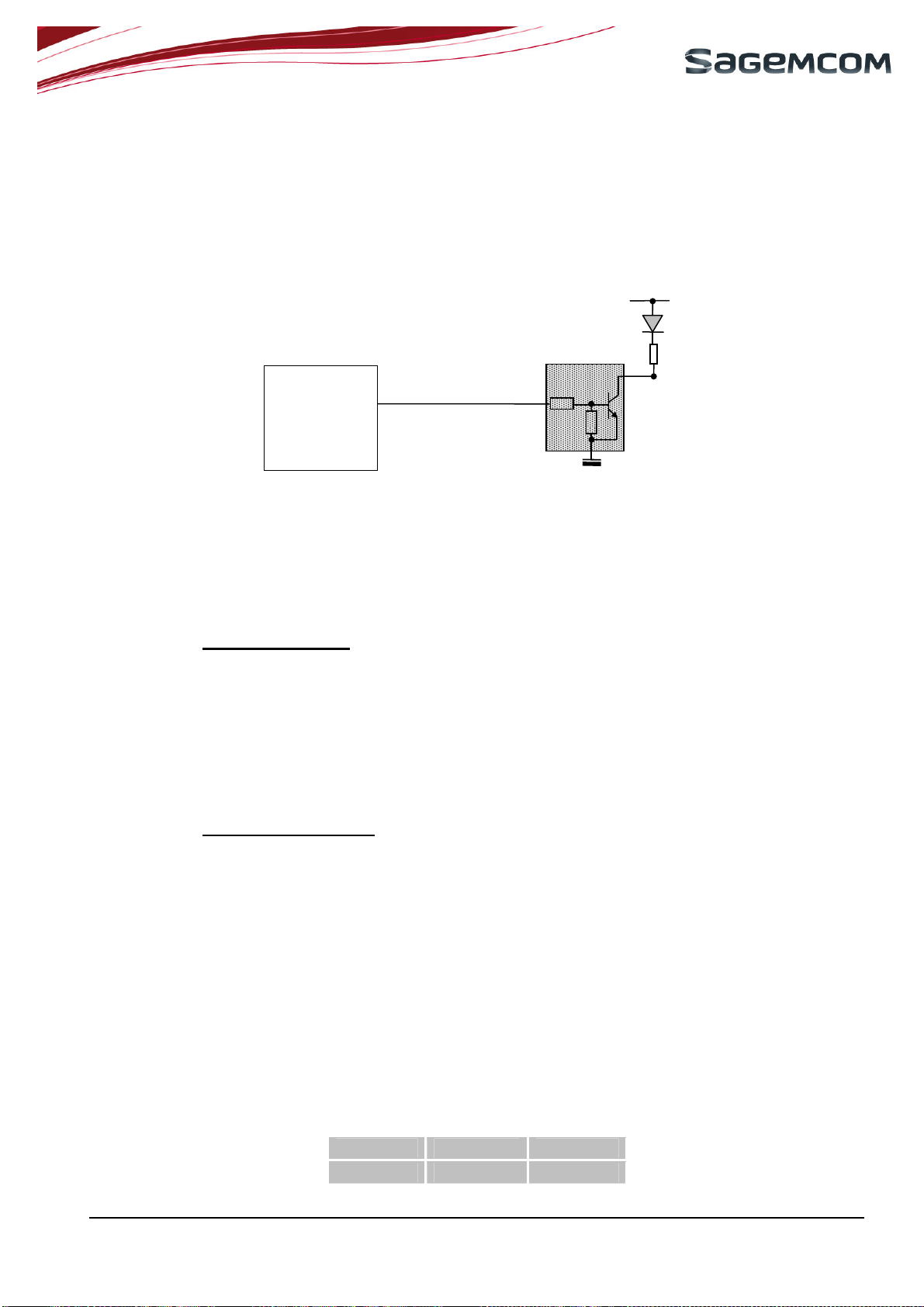
3.4 NETWORK LED
The HiLo V2 module can manage a network LED. The LED can be connected either to one of the available
GPIO or to a PWM (but not the one dedicated to the buzzer).
The transistors can be found a in a single package referenced as UMDXX or PUMDXX Family.
Value of resistor R depends on characteristic of chosen LED; it is used to limit the current through the diode.
Use the AT command to set the GPIO or PWM used to control the LED.
GPIO or
PWM
HiLo V2
VBAT
R
Figure 12: Network LED connection
3.5 POWER SUPPLY
The HiLo V2 module can be supplied by a battery or any DC/DC converter compliant with the module supply
range 3.2V to 4.5V and 2.2 A.
WARNING:
The HiLo V2 module is not supposed to be supplied with a voltage over 4.5V even in transient.
However the module can resist to over voltage transient lower than 6.8V.
If the system main board power supply unit is not stable or if the system main board is supplied with 9V
or over, in case of transient voltage presence on the circuit, the HiLo V2 module power amplifier may be
severely damaged.
To avoid such issue, simply add a voltage limiter to the module power supply lines so the VBATT signal Pins
may never receive a surge voltage over 6.8V. The limiter can be as simple as a Zener diode as shown here
under or in the annex development kit schematic of this document.
Figure 13: Over voltage protection on VBatt
The PCB tracks must be well dimensioned to support 2.2 A maximum current (Burst current 1.8A plus the
extra current for the other used I/Os). The voltage ripple caused by serial resistance of power supply path
(Battery internal resistance, tracks and contact resistance) could result in the voltage drops.
To prevent any issue in the power up procedure the typical rise time for VBAT should be 1ms.
Note d’étude / Technical document :
URD1– OTL 5635.2– 007 / 72335 Edition 01
HiLo V2 Application Note
15 March 2011 - Page 16/58
Page 17

The HiLo V2 module does not manage the battery charging.
3.5.1 Burst conditions
- Communication mode (worst case: 2 continuous GSM time-slot pulse):
Figure 14: GSM/GPRS Burst Current rush
A 47µF with Low ESR capacitor is highly recommended for VBAT and close to the module Pins1,2 & 39,40.
3.5.2 Ripples and drops
Current burst at 1.8A 33dBm
GSM TX Lev 5
Ripple
VBAT drop
3.2V Min
Figure 15: GSM/GPRS Burst Current rush and VBAT drops and ripples
The minimum voltage during the drop of VBAT must be 3.2V at 33dBm at Pins1,2,39 & 40 for the full range
of the required functioning temperature. To reach this aim, adapt the VBAT tracks width to minimize the loss:
the shorter and thicker is the track, the lower is the serial impedance.
To check the serial resistor, any CAD software can be used or by experiment by measuring it on the PCB by
injecting 1A into the VBAT track on connector side and shorting to GND the other side, this could be done using
a laboratory power supply set to few volts with a limitation in current to 1A. Then the measure of the drop
voltage leads to the serial resistor.
Noise on VBAT due to drops could result in poor audio quality.
Serial resistor should be less than 250mΩ including the impedance of connectors if any.
Ripple has to be minimised to have a clean RF signal. This can be improved by filtering the output of the
power supply when AC/DC or DC/DC components are used. Refer to the power converter chip supplier
application note for more information and advises.
Note d’étude / Technical document :
URD1– OTL 5635.2– 007 / 72335 Edition 01
HiLo V2 Application Note
15 March 2011 - Page 17/58
Page 18

To have 3.7V out R1=560K & R2=271.8K
(270K+1.8K)
3.6 EXAMPLE OF POWER SUPPLIES
3.6.1 DC/DC Power supply from a USB or PCMCIA port.
It the following application note from Linear Technology LTC3440, this schematic is an example of a DC/DC
power supply able to power 3.6V under 2A. This can be use with a AC/DC 5V unit or an USB or PCMCIA bus as
input power source. C6 to C9 can be followed by a serial MOS transistor to avoid a slow rise signal at VOUT.
Figure 16: Example of power supply based on a DC/DC step down converter
3.6.2 Simple high current low dropout voltage regulator.
If the whole power consumption is not an issue, this example of a simple voltage regulator preceded by an
AC/DC to 5V converter, can be use to power the module.
The voltage output is given by:
VOUT = 1.235V × [1 + (R1 / R2)]
Figure 17: Example of power supply based on regulator MIC29302WU
Note d’étude / Technical document :
URD1– OTL 5635.2– 007 / 72335 Edition 01
HiLo V2 Application Note
15 March 2011 - Page 18/58
Page 19

3.6.3 Simple 4V boost converter.
Simple boost converter with Linear LT1913 (see LT1316 evaluation kit document). The input can be preceded
by an AC/DC converter to get the 5V. PGOOD signal can be checked before the ignition of the module.
Figure 18: Example with Linear LT1913
3.7 UART
The HiLo V2 module features a V24 interface to communicate with the host through AT commands or for easy
firmware upgrading purpose.
It is recommended to manage an external access to the V24 interface, in order to allow easy software
upgrade (baud rate up to 460.8kbps, validated with ATEN USB/Serial converter).
DTR, DSR, DCD and RI signals are internally pull upped to VGPIO with a 100KΩ.
RI signal is a stand alone signal that can be used with anyone of the following configurations. Consult the
AT command specification for more information about this signal and its use.
3.7.1 Signals reminder
The following table quickly sums up the use of the different signals from UART
Signal name Signal use(DTE point of view)
RX
TX
DCD
DSR
DTR
RTS
CTS
RI
Note d’étude / Technical document :
URD1– OTL 5635.2– 007 / 72335 Edition 01
Receive data
Transmit data
Signal data connections in progress (GPRS or CSD)
Signal UART interface is ON
Prevent the HiLo V2 to enter into sleep mode
Switch between data and command modes
Wake up the module,…
Wakes up the module when Ksleep=1 is used
Signal HiLo V2 is ready to receive AT commands, has waken up
Signal incoming calls (voice and data), SMS,…
HiLo V2 Application Note
15 March 2011 - Page 19/58
Page 20

Consult the AT command Specification document for the use of the UART signals.
Unused signals can be left not connected.
3.7.2 Complete V24 – connection HiLo V2 - host
A V24 interface is provided on the 40 pads of the HiLo V2 module with the following signals: RTS/CTS,
RXD/TXD, DSR, DTR, DCD, RI.
The use of this complete V24 connection is recommended as soon as your application needs to exchange
data (over GPRS or CSD).
HiLo V2 Module
13
14
11
12
28
29
26
27
TXD
CTS
DSR
DCD
RI
DTR
RXD
RTS
RXD
CTS
DSR
DCD
RI
DTR
TXD
RTS
DTE Device
2.8V signals
Note: GND is not
represented
DCE point of view
Figure 19: Complete V24 connection between HiLo V2 and host
This configuration allows to use the flow control RTS & CTS to avoid any overflow error during the data transfer,
CTS is moreover used to signal when the HiLo V2 is ready to receive an AT command after a power up
sequence or a wake up from sleep mode.
This configuration allows as well all the signalling signals like:
• RI signal used when programmed to indicate an incoming voice or data call or SMS incoming etc…
• DCD signal used to signal the GPRS connections
• DSR signal used to signal the module UART interface is ON
• DTR signal used to prevent the HiLo V2 module from entering into sleep mode or to switch between
Data and AT commands or to hang up a call or to wake up the module etc…
DTE point of view
2.8V signals
Figure 20: CTS versus POK_IN signal during the power on sequence.
Note d’étude / Technical document :
URD1– OTL 5635.2– 007 / 72335 Edition 01
HiLo V2 Application Note
15 March 2011 - Page 20/58
Page 21
1
6
9
5
Avoid supplying the UART before the HiLo V2 module is ON, this could result in bad power up sequence.
3.7.3 Complete V24 interface with PC
It supports speeds up to 115.2 Kbps and may be used in auto bauding mode.
To use the V24 interface, some adaptation components are necessary to convert the +2.8V signals from the
HiLo V2 to +/- 5V signals compatible with a PC.
HiLo V2 Module
13
14
11
12
28
29
26
27
2.8V signals
DCE point of view
TXD
CTS
DSR
DCD
RI
DTR
RXD
RTS
RS232 Transceiver
IN
IN
IN
IN
IN
OUT
OUT
OUT
3.1V to +/-5.5V
Figure 21: connection to a data cable
OUT
OUT
OUT
OUT
OUT
IN
IN
IN
signals
RXD
CTS
DSR
DCD
RI
DTR
TXD
RTS
DTE point of view
2
8
6
1
9
4
3
7
SUBD9 Female
Note: pin 5 is GND
Avoid supplying the UART before the HiLo V2 module is ON, this could result in bad power up sequence.
To have a proper behaviour use the signal VGPIO to enable the RS232 Transceiver.
To create your own data cable (for software download purpose…etc…) refer to the following schematic as an
example with a MAX3238E:
• VCC_3V1 is an LDO output (VBAT to VCC_3V1) enabled by VGPIO from the module.
• 180Ω are serial resistors aimed to limit the EMC and ESD propagation.
Note d’étude / Technical document :
URD1– OTL 5635.2– 007 / 72335 Edition 01
HiLo V2 Application Note
15 March 2011 - Page 21/58
Page 22

Figure 22: Example of a connection to a data cable with a MAX3238E
3.7.4 Partial V24 (RX-TX-RTS-CTS) – connection HiLo V2 - host
When using only RX/TX/RTS/CTS instead of the complete V24 link, the following schematic could be used.
HiLo V2 Module
TXD
13
CTS
14
DSR
11
DCD
12
RI
28
DTR
29
RXD
26
27
RTS
2.8V signals
DCE point of view
Figure 23: Partial V24 connection (4 wires) between HiLo V2 and host
Note: GND is not
represented
RXD
CTS
DSR
DCD
RI
DTR
TXD
RTS
DTE point of view
DTE Device
2.8V signals
As DSR is active (low electrical level) once the HiLo V2 is switched on, DTR is also active (low electrical
level), therefore AT command AT+Ksleep can switch between the two sleeps mode available for the HiLo V2.
DTR input signal is internally pull upped to VGPIO with a 100KΩ, this result in 28µA of extra consumption.
DCD and RI can stay not connected and floating when not used.
Note d’étude / Technical document :
URD1– OTL 5635.2– 007 / 72335 Edition 01
HiLo V2 Application Note
15 March 2011 - Page 22/58
Page 23

RI signal is a stand alone signal that can be used with anyone of the following configuration. Consult the
AT command specification for more information about this signal and its use.
This configuration allows to use the flow control RTS & CTS to avoid any overflow error during the data transfer,
CTS is moreover used to signal when the HiLo V2 is ready to receive an AT command after a power up
sequence or a wake up from sleep mode.
Figure 24: CTS versus POK_IN signal during the power on sequence.
However this configuration does not allow the signalling signals like:
• RI signal used when programmed to indicate an incoming voice or data call or SMS incoming etc…
• DCD signal used to signal the GPRS connections
• DSR signal used to signal the module UART interface is ON
• DTR signal used to prevent the HiLo V2 module from entering into sleep mode or to switch between
Data and AT commands or to hang up a call or to wake up the module etc…
Consult the AT command Specification document for the uses of the UART signals.
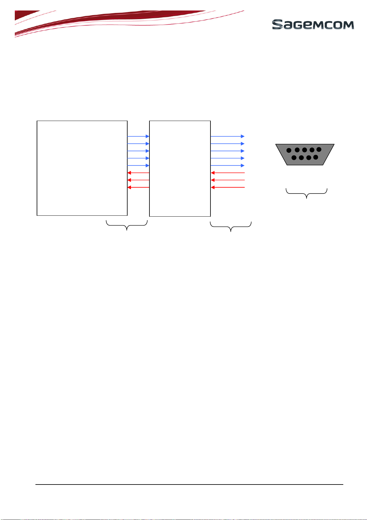
3.7.5 Partial V24 (RX-TX) – connection HiLo V2 - host
When using only RX/TX instead of the complete V24 link, the following schematic could be used.
HiLo V2 Module
13
14
11
12
28
29
26
27
TXD
CTS
DSR
DCD
RI
DTR
RXD
RTS
RXD
CTS
DSR
DCD
RI
DTR
TXD
RTS
DTE Device
2.8V signals
DCE point of view DTE point of view
Figure 25: Partial V24 connection (2 wires) between HiLo V2 and host
Note d’étude / Technical document :
URD1– OTL 5635.2– 007 / 72335 Edition 01
Note: GND is not
represented
2.8V signals
HiLo V2 Application Note
15 March 2011 - Page 23/58
Page 24

As DSR is active (low electrical level) once the HiLo V2 is switched on, DTR is also active (low electrical
level), therefore AT command AT+Ksleep can switch between the two sleep modes available for the HiLo V2.
DTR input signal is internally pull upped to VGPIO with a 100KΩ, this result in 28µA of extra consumption.
As CTS is active (low electrical level) once the HiLo V2 is switched on, RTS is also active (low electrical
level), therefore AT command AT+Ksleep can switch between the two sleep modes available for the HiLo V2.
The HiLo V2's firmware allows the rise of CTS during the sleep state even when looped to RTS signal.
DCD and RI can stay not connected and floating when not used.
RI signal is a stand alone signal that can be used with anyone of the following configuration. Consult the
AT command specification for more information about this signal and its use.
This configuration does not allow to use the flow control RTS & CTS. Those signals are used to avoid any
overflow error during the data transfer, CTS is moreover used to signal when the HiLo V2 is ready to receive an
AT command after a power up sequence or a wake up from sleep mode.
Figure 26: CTS versus POK_IN signal during the power on sequence.
Moreover this configuration does not allow the signalling signals like:
• RI signal used when programmed to indicate an incoming voice or data call or SMS incoming etc…
• DCD signal used to signal the GPRS connections
• DSR signal used to signal the module UART interface is ON
• DTR signal used to prevent the HiLo V2 module from entering into sleep mode or to switch between
Data and AT commands or to hang up a call or to wake up the module etc…
Consult the AT command Specification document for the uses of the UART signals.
3.8 UART0
HiLo V2 module manages a 2-wire UART interface. This UART interface is only dedicated for software traces.
Sagemcom strongly recommends leaving this interface externally accessible for trace (e.g. access by test
point pads).
Note d’étude / Technical document :
URD1– OTL 5635.2– 007 / 72335 Edition 01
HiLo V2 Application Note
15 March 2011 - Page 24/58
Page 25

3.9 GPIO
There are Three GPIOs available on HiLo V2. All GPIOs have internal pull-up resistors.
GPIOs can directly be controlled with dedicated AT commands.
Thanks to some other special AT commands, GPIOs can for example be used :
• to make an I/O toggling while the module is attached to the network
• to make an I/O toggling when a programmed temperature is reached
• as input to detect the presence of an antenna (with some external additional electronic)
• as input to detect the SIM card presence …etc
3.10 ADC
There is one ADC input pad which can be used to read the value of the voltage applied. Following
characteristics must be met to allow proper performances:
• The input signal voltage must be within 0V and up to 3V
• The input impedance of the pad is 150KΩ
• The input capacitance is typically 10pF.
The AT command AT+KADC will give voltage value with following characteristics:
• 10 bits resolution
• Maximum sampling frequency is 200KHz.
Consult the AT command Specification document for more information about KADC AT command.
3.11 PCM
There is a master PCM interface available on HiLo V2. The PCM interface can be configured by dedicate AT
commands. Following characteristics must be met:
• 16 bits PCM data word length
• Configurable PCM clock rate must not exceed 1MHz
Figure 27: PCM interface timing
Note d’étude / Technical document :
URD1– OTL 5635.2– 007 / 72335 Edition 01
HiLo V2 Application Note
15 March 2011 - Page 25/58
Page 26
3.12 RF BURST INDICATOR
There is one digital output named RF_TX available on HiLo V2 to indicate the RF transmission. This output can
not be controlled by AT commands and can not be used for other purpose.
This output can only connect to a transistor but not to drive a LED directly. Otherwise, the RF
transmission will be unexpectedly affected.
VBAT
R
RF_TX
HiLo V2
Figure 28: RF_TX burst indicator
3.13 BACKUP BATTERY
3.13.1 Backup battery function feature
3.13.1.1 With backup battery
A backup battery can be connected to the module in order to supply internal RTC (Real Time Clock) when the
main power supply is removed. Thus, when the main power supply is removed, the RTC is still supplied and the
module keeps the time register running.
With external backup battery:
• If VBAT < 3V, internal RTC is supplied by VBACKUP.
• If VBAT ≥3V, internal RTC is supplied by VBAT.
3.13.1.2 Without backup battery
Without backup battery
• If VBAT ≥ 1.5V, internal RTC is supplied by VBAT.
• If VBAT < 1.5V, internal RTC is not supplied.
VBACKUP input of the module has to be connected to a 10µF capacitor (between VBACKUP and GND).
Sagemcom does not recommend to connecting VBACKUP signal to VBAT as for former Sagemcom
MOXX modules.
3.13.2 Current consumption on the backup battery
When the power supply is removed, the internal RTC will be supplied by backup battery.
To calculate the backup battery capacity, consider that current consumption for RTC on the backup
battery is up to 1000µA depending on the temperature.
Pad Name
VBACKUP
Note d’étude / Technical document :
URD1– OTL 5635.2– 007 / 72335 Edition 01
Min Max
1000µA
HiLo V2 Application Note
15 March 2011 - Page 26/58
Page 27

3.13.3 Charge by internal HiLo V2 charging function
The charging function is available on the HiLo V2 without any additional external power supply (the charging
power supply is provided by the HiLo V2).
Charge of the back-up battery occurs only when main power supply VBAT is provided.
The recommended schematic is given hereafter:
VBACKUP
R
VBACKUP
HiLo V2
Backup battery
HiLo V2
10µF capacitor
Figure 29: Backup battery or 10µF Capacitor internally charged
The resistor R depends on the charging current value provided by the battery manufacturer.
The charging curve which is done by the HiLo V2 is given hereafter:
Figure 30: Charging curve of backup battery
3.13.4 Backup Battery technology
3.13.4.1 Manganese Silicon Lithium-Ion rechargeable Battery
Sagemcom does not recommend using this kind of technology because of the following drawbacks:
• The maximum discharge current is limited (Shall be compliant with the module characteristics).
• The over-discharge problem: most of the Lithium Ion rechargeable batteries are not able to recover their
charge when their voltage reaches a low-level voltage. To avoid this, it is necessary to add a safety
component to disconnect the backup .battery in case of over–discharge condition. In such a case, this
implementation is too complicated (too much components for that function).
• The charging current has to be regulated.
Sagemcom does not recommend using this kind of backup battery technology.
Note d’étude / Technical document :
URD1– OTL 5635.2– 007 / 72335 Edition 01
HiLo V2 Application Note
15 March 2011 - Page 27/58
Page 28

3.13.4.2 Capacitor battery
These kinds of backup battery have not the drawbacks of the Lithium Ion rechargeable battery.
As there are only capacitors:
• The maximum discharge current is generally bigger,
• There is no problem of over-discharge: the capacitor is able to recover its full charge even if its voltage
has previously fallen to 0V.
• There is no need to regulate the charging current.
Moreover, this kind of battery is available in the same kind of package than the Lithium Ion cell and fully
compatible on a mechanical point of view. The only disadvantage is that the capacity of this kind of battery is
significantly smaller than Manganese Silicon Lithium Ion battery. But for this kind of use (supply internal RTC
when the main battery is removed), the capacity is generally enough.
Sagemcom strongly recommends using this kind of backup battery technology.
3.14 START THE MODULE PROPERLY AND AVOID POWER UP ISSUES
This chapter gives advices on how to make a proper start of the HiLo V2 module and sums up the side effects
of a non compliant power up sequence or a non compliant hardware connection between the HiLo V2 and the
host CPU.
3.14.1 Power domains
Each HiLo V2 pad is linked to a specific internal power domain as the following:
• VANA is typically 2.85V and is a general purpose analogue dedicated voltage.
• VBAT is typically 3.2V to 4.5V and is the main system voltage.
• VRTC is typically 3.0V and is the real time clock dedicated voltage.
• VGPIO is typically 2.8V and is a general purpose digital dedicated voltage.
• VSIM is typically 1.8V or 2.9V and is the digital SIM card function dedicated voltage.
• VPERM is typically 3.0V and is the permanent voltage dedicated to launch the power up sequence.
Figure 31 provides for each 40pins of the HiloV2 the corresponding power domain.
Note d’étude / Technical document :
URD1– OTL 5635.2– 007 / 72335 Edition 01
HiLo V2 Application Note
15 March 2011 - Page 28/58
Page 29

HiLo V2
Pins
Signal Name Function Power domain
1 VBATT POWER 3.7V
2 VBATT POWER 3.7V
3 GND POWER 0V
4 GND POWER 0V
5 /UART0_TXD UART 0 2.85V
6 /UART0_RXD UART 0 2.85V
7 /RF_TX RF 2.8V
8 /GPIO3 GPIO 2.8V
9 /GPIO2 GPIO 2.8V
10 VGPIO EXT_VDD 2.8V
11 /UART1_DSR UART 1 2.8V
12 /UART1_DCD UART 1 2.8V
13 /UART1_TXD UART 1 2.85V
14 /UART1_CTS UART 1 2.85V
15 /SIM_RST SIM 1.8V or 2.9V
16 /SIM_CLK SIM 1.8V or 2.9V
17 /PWM0 PWM 2.85V
18 /RESET_IN RESET 2.8V
19 /AUX_ADC0 ADC 2.85V
20 /INTMIC_P AUDIO 2.85V
21 /HSET_OUT_P AUDIO 3.7V
22 /HSET_OUT_N AUDIO 3.7V
23 /PWM1 PWM 2.85V
24 VSIM SIM 1.8V or 2.9V
25 /SIM_DATA SIM 1.8V or 2.9V
26 /UART1_RXD UART 1 2.85V
27 /UART1_RTS UART 1 2.85V
28 /UART1_RI UART 1 2.8V
29 /UART1_DTR UART 1 2.8V
30 VBACKUP EXT_VDD 3.0V
31 /POK_IN POWER ON 3.0V
32 /GPIO1 GPIO 2.8V
33 /PCM_OUT PCM 2.85V
34 /PCM_IN PCM 2.85V
35 /PCM_SYNC PCM 2.85V
36 /PCM_CLK PCM 2.85V
37 GND POWER 0V
38 GND POWER 0V
39 VBATT POWER 3.7V
40 VBATT POWER 3.7V
Figure 31 : HiLo V2 40 pins with their power domains
Note d’étude / Technical document :
URD1– OTL 5635.2– 007 / 72335 Edition 01
HiLo V2 Application Note
15 March 2011 - Page 29/58
Page 30

3.14.2 IO DC presence before power ON.
When the VBAT is available but the module not yet started, the following I/O's raised their output.
• VBACKUP raise to 3V
• POK_IN raise to 3V
• HSET_N raise to 1.4V
• HSET_P raise to 1.4V
3.14.3 Side effects of a retro supply (current re-injection)
Interactions or connections between the HiLo V2 module and the external systems can lead to retro power
supply side effects, or current re-injection through pads while the module is not yet fully powered up (means
VBAT lower than its minimum 3.2V).
If some precaution and simple rules are not followed, those effects can in worst case result in a deadlock
module, not able to start up or to communicate.
Deadlock could happen if the retro supply occurs before the module start. The flow back current could in the
worst case prevent the module to start.
The very same behaviour can happen in a normal use conditions when the lines connecting to the module to the
external system uses a non compliant voltage higher than the module IO power domain (2.85V). This results in
a current flow back inside the module and can lead to a deadlock system on the next start if this retro supply
has continued while the system was powered off or under powered (under 3.2V).
An over voltage on any line can also damage the HiLo V2 module.
Those consequences are very rare but exist. Therefore, the rules and advises given on every chapter of this
application note must be followed.
To avoid any power up issue, here are the rules:
Avoid any over voltage on the buses lines connected to the module.
When the module is off, do not apply any voltage on lines connected to the module.
The over voltage can be avoided by using the same power domain voltage.
Avoid 5V or 3.3V systems straight connection to 2.8V HiLo V2 lines.
Use level adaptors when the power domain requires it.
When the module is off:
Power off the buses lines of the main system that are connected to the module, this avoid any flow back
current (re-injection) and of course help a lot to improve and control the power consumption. This last issue is
important as in off mode there is not control of the current inside the module and can results in a loss of current
by leakage through the I/Os of the module.
3.14.4 Example of a Current re-injection on U.A.R.T.
Current re-injection appears when the module is off or not powered and I/Os connected to the module still
powered. Example: UART bus powered from the DTE side before the module is powered. This can result in a
bad starting behaviour.
To avoid current re-injection, simply do not supply the lines connected to the module before the module
switches on. Power up the module first using the POK_IN Line then open the UART lines for the DTE side and
all necessary I/O, this will avoid leakage of current improving the power consumption and avoid any possible
deadlock issue during the power up process.
Note d’étude / Technical document :
URD1– OTL 5635.2– 007 / 72335 Edition 01
HiLo V2 Application Note
15 March 2011 - Page 30/58
Page 31

Power supply domain
I max = 15mA
Clamp
Diode
IN Buffer
Clamp
Diode
OUT Buffer
Vd = 0.4V
Pin_X
Vd = 0.4V
I max = 15mA
Figure 32: Digital Pin-out clamp diode
All the digital pins have this structure a current re-injection by supplying the lines with a non compliant
voltage range must be avoided. (From -0.4V up to 2.8V+0.4V)
Reverse currents over 15mA will damage the chip. Avoid this issue. Keep the connected line voltage
between 0 and 2.8V.
For an interface with a CMOS 3.3V system or TTL 5V system, use level adapters powered by 2 supplies:
a 2.8V from a LDO IC which is enabled by VGPIO signal and the other external required voltage 3.3V or 5V.
If a Level shifter is used or a RS232 adapter, use the VGPIO signal as the enable signal to avoid any
current re-injection before the module start.
If a straight connection is used between the HiLo V2 and the DTE UART it is necessary to isolate host
and HiLo V2 module in order to avoid to generate current re-injection through when HiLo V2 is switched-off.
Example of schematic (only useful signals are represented):
DTR, RTS, RXD
HiLo V2
DCD, DSR, CTS, TXD, RI
Figure 33: Hardware interface diodes solution between HiLo V2 and host
HiLo V2
DTR, RTS, RXD
DCD, DSR, CTS, TXD, RI
Figure 34: Hardware interface buffers solution between HiLo V2 and host
Note d’étude / Technical document :
URD1– OTL 5635.2– 007 / 72335 Edition 01
VGPIO
Buffer
Host
Tri state command
Host
HiLo V2 Application Note
15 March 2011 - Page 31/58
Page 32

3.14.5 Advices for every power domain
• To avoid any current re-injection on VANA (2.85V)
If an external bias voltage over VANA is used for the microphone, use a 10µF serial capacitor to block the
DC voltage.
If a voltage higher than VANA has to be measured by the ADC, use external resistor divider to limit it.
if PWM bus is output only, the external system is supposed to be in input on the same voltage domain, if it is
not the case or if its inputs are pulled up and able to source current while the module is off, then simply use
open drain or open collector transistors to avoid any flow back current to the module.
The external system connected to the module by the UART has to switch its UART lines off while the module
is off. If the external system cannot commands its UART lines off, then it is necessary to add a buffer between
the module and the external system to prevent any issue. In this last case, the buffer would have to be enabled
by the VGPIO voltage that is only available when the module starts. This applies to TXD, RXD, RTS, CTS which
are on this power domain and also to the lines on the VGPIO power domain (see here after).
• To avoid any current re-injection on VGPIO (2.80V)
Do not connect a power supply to the VGPIO pad. This pad is an LDO output only.
The reset signal is internally pulled up and can be connected to an open drain transistor.
The GPIOs have to be used in compliance of the power domain and when the module is off, the external
system has to shut off its GPIOs.
The SPI bus has to be not connected to the external system.
The JTAG bus has to be not connected to the external system.
The UART lines on this power domain (DCD, DTR, DSR, RI) have to follow the same rules as those on
VANA domain (TXD, RXD, RTS, CTS). See have above.
A resistor of 10KΩ has to be connected to the NTRST pad and GND to pull down this I/0, preventing any
deadlock due to VGPIO current re-injection.
• To avoid any current re-injection on VPERM (3.0V)
The POK_IN signal is internally pulled up and can be connected to an open drain transistor.
• To avoid any current re-injection on VRTC (3.0V)
The VBACKUP signal has to be only connected to a DC coin 3V battery or a capacitor of 10µF.
• To avoid any current re-injection on VSIM (1.8V or 2.9V)
Use only VSIM pads to supply the sim card or sim chip.
• To avoid any current re-injection on VBAT (3.2V to 4.5V)
Use a VBAT signal with a fast rise time to have a VBAT final value as fast as possible. (see hereafter)
In case of needs, use 2 serial capacitors of 10µF to connect the audio speaker lines to the external system
inputs.
3.14.6 CASE OF VBAT RISE TIME
The VBAT rise time from 0V to its final value has to be lower than 1ms
possible failure during the power up. If this value cannot be guaranteed, then some MOS transistors could be
used to create a fast rise time switch able to quickly commute from the VBAT final value to the modules power
pads.
(1)
This value will be updated to a higher final value including the worst case.
(1)
. This is necessary in order to avoid any
3.14.7 Start- up
To start the module, first power up VBAT, which must be in the range 3.2V ~ 4.5V, and able to provide 2.2A
during the TX bursts
(Refer to the module specification for more details).
POK_IN is a low level active signal internally pulled up to a dedicated power domain to 3V.
As POK_IN is internally pulled up, a simple open collector or open drain transistor can be used for ignition.
Warning: The POK_IN will become low after module is ready. An open collector or open drain transistor
must be used. The POK_IN can not be directly driven by a GPIO signal.
Note d’étude / Technical document :
URD1– OTL 5635.2– 007 / 72335 Edition 01
HiLo V2 Application Note
15 March 2011 - Page 32/58
Page 33

commands
Max 7 seconds
To start the module, a low level pulse must be applied on POK_IN during 2000 ms.
RESET must not be Low during that period of time
After a few seconds, the CTS goes to the active state when the module is ready to receive AT commands.
VGPIO is a supply output from the module that can be used to check if the module is alive.
• When VGPIO = 0V the module is OFF
• When VGPIO = 2.8V the module is ON (It can be in Idle, communication or sleep modes)
Module is
OFF
CTS
2000ms
POK_IN
Software Loading
spike
Typ 5 seconds
Figure 35: Power ON sequence
Module is
ON
VGPIO
Module is ready
to receive AT
3.15 UART SIGNALS AT POWER ON
The UART signals are low level active therefore these signals rise up when the module starts. During around
70ms (see Figure 36), those signals present a transient spike. Those spikes behaviour at start up are normal,
however pay attention to them when a CTS low level detection is used do send AT commands. Only DSR and
CTS signals get low after the end of the start up procedure.
Note d’étude / Technical document :
URD1– OTL 5635.2– 007 / 72335 Edition 01
HiLo V2 Application Note
15 March 2011 - Page 33/58
Page 34

TXD
RXD
DTR
RI
DCD
DSR
RTS
Max 7 seconds
70ms
30ms
150ms
OFF
POK_IN
CTS
Module is
2000ms
Module is ON
Module UART
interface is ON
Module is ready to
receive AT commands
Typ 5 seconds
Transients spikes
during power on
sequence
Figure 36: Full UART signals during the power on sequence.
Note d’étude / Technical document :
URD1– OTL 5635.2– 007 / 72335 Edition 01
HiLo V2 Application Note
15 March 2011 - Page 34/58
Page 35

send AT
3.16 POWER ON AND SLEEP DIAGRAMS
Those 2 diagrams show the behaviours of the module and the DTE during the power on and then in the sleep
modes.
DTE is in idle mode
U.A.R.T.
closed ?
VBAT≥3.2
Volts min
POK_IN
LOW for 2s
AND Reset
High?
KSUP notified if KSREP
VGPIO rise to 2.8V
CTS is Low and /or
activated
Figure 37: Diagram for the power on
Note d’étude / Technical document :
URD1– OTL 5635.2– 007 / 72335 Edition 01
Module is ready
to receive and
HiLo V2 Application Note
15 March 2011 - Page 35/58
Page 36

or the OS
mode
Module is ready to
receive and send AT
Sleep mode request
Ksleep = 1 OR
( Ksleep = 0
AND
DTR = High)
Delay to enter the sleep
mode
DTE could also
be in sleep
VGPIO remains at 2.8V
Module is in
sleep mode
Wake up incoming event such as:
RI signal
connected
and
programmed?
CTS is High
The wakes up
periods are set by
the network DRX
• Network event.
• Alarm interruption.
• DTR interruption.
• RTS interruption.
Figure 38: Diagram for the sleep mode
Note d’étude / Technical document :
URD1– OTL 5635.2– 007 / 72335 Edition 01
RI wakes the DTE
DTE is in idle mode
HiLo V2 Application Note
15 March 2011 - Page 36/58
Page 37

GPIO
3.17 MODULE RESET
To reset the module, a low level pulse must be sent on RESET pin during 10 ms. This action will immediately
restart the HiLo V2 module. It is therefore useless to perform a new ignition sequence (POK_IN) after.
Sagemcom recommends using this feature in case of emergency, freeze of module or abnormal longer
time to respond to AT Commands, this signal is the only way to get the control back over the HiLo V2 module.
RESET is a low level active signal internally pulled up to a dedicated power domain.
As RESET is internally pulled up, a simple open collector or open drain transistor can be used to control it.
2.4V min
2.8V
RESET_IN: 18
HiLo V2 Module
DCE
Figure 39: Reset command of the HiLo V2 by an external GPIO
The RESET signal will reset the registers of the CPU and reset the RAM memory as well.
As RESET is referenced to VGPIO domain (internally to the module) it is impossible to make a reset
before the module starts or try to use the RESET as a way to start the module.
An other solution more costly would be to use MOS transistor to switch off the power supply and restart the
power up procedure using the POK_IN input line.
0.4V max
10ms
HOST DTE
3.18 MODULE SWITCH OFF
AT command “AT*PSCPOF” allows to switch off "properly" the HiLo V2 module.
In case of necessary the module can be switched off by controlling the power supply. This can be used for
example when the system freezes and no reset line is connected to the HiLo V2. In this case the only way to get
the control back over the module is to switch off the power line. If the system is on a battery, it is wise to have a
control of the power supply by a GPIO with for example the following schematic.
Figure 40: Power supply command by a GPIO
Note d’étude / Technical document :
URD1– OTL 5635.2– 007 / 72335 Edition 01
HiLo V2 Application Note
15 March 2011 - Page 37/58
Page 38

This kind of schematic could also be used to save few micro amperes in case of need. As the module has
a drain current of up to 56µA, this kind of function could lower it to the current through R4.
These, are the behaviours of the VGPIO and the CTS signal during the power off sequence.
AT*PSCPOF
Module is ON
POK_IN is low
Module is OFF
POK_IN is high
Typ 2 seconds
VGPIO
CTS
Figure 41: Power OFF sequence for POK_IN, VGPIO and CTS
3.19 SLEEP MODE MANAGEMENT AND POWER CONSUMPTION
The AT command “AT+KSLEEP” allows to configure the sleep mode.
When AT+KSLEEP=1 is configured:
• The HiLo V2 module decides by itself when it enters in sleep mode (no more task running).
• “0x00” character on serial link wakes up the HiLo V2 module.
When AT+KSLEEP=0 is configured:
• The HiLo V2 module is active when DTR signal is active (low electrical level).
• When DTR is deactivated (high electrical level), the HiLo V2 module enters in sleep mode after a while.
• On DTR activation (low electrical level), the HiLo V2 module wakes up.
When AT+KSLEEP=2 is configured:
• The HiLo V2 module never enters in sleep mode.
In sleep mode the module reduces its power consumption and remains waiting for the wake up signals either
from the network (i.e. Read paging block depending on the DRX value of the network) or the operating system
(i.e. timers wake up timers activated) or the host controller (i.e. character on serial link or DTR signal).The
power consumption should look like the following example for DRX9.
Note d’étude / Technical document :
URD1– OTL 5635.2– 007 / 72335 Edition 01
HiLo V2 Application Note
15 March 2011 - Page 38/58
Page 39

Figure 42: Power consumption at DRX9 (with RS-NGMO2 power supply)
When the HiLo V2 module leaves the sleep mode thanks to the network incoming signal or by action of the user
the power consumption will step from the <1.7mA to 15mA and then to 25mA in around 2 seconds.
The behaviour of the system at wake-up:
• System resumes from clock 32Mhz, the power consumption rises to around 15mA.
• System resumes the hardware blocks, the power consumption rises to around 25mA.
To perform the correct measurement of the power supply of a system using a HiLo V2 module, refer to
the specification TW0.9 version 4.7 June 2008 chapter "standby test procedure" from the GSM
association. This specification explains how to proceed and what apparatus have to be used to perform
the test.
Check also Sagemcom document "Getting started with the current consumption measurement"
The main parameters for a compliant measurement are:
Parameter Idle Mode Setting Idle Mode Setting
Measurement Serial Resistance 0.5 ohms
Tolerance/Type. 1%, 0.5W, high precision metal film resistor
Sampling frequency 50 k samples/s
Resolution 0.1mA over the full dynamic range of module currents
Noise floor Less than lowest ADC step
Note d’étude / Technical document :
URD1– OTL 5635.2– 007 / 72335 Edition 01
HiLo V2 Application Note
15 March 2011 - Page 39/58
Page 40

4. RECOMMENDED I/OS AND COMPONENTS ON THE FINAL PRODUCT
The design of the customer’s board (on which the module is soldered) must provide an access to following
signals when the final product will be completely integrated.
To upgrade the module software, Sagemcom recommends providing a direct access to the module serial
link through an external connector or any mechanism allowing the upgrade of the module without opening
the whole product.
Serial link:
TXD Output UART transmit
RXD Input UART receive
To trace the module software, Sagemcom recommends providing a direct access to the module trace port
UART0 (2 I/Os) through internal test points (TP) located on the customer's main board.
The board has to feature as minimum those external components.
A capacitor of 47µF on the VBAT near Pins1,2 & 39,40.
A capacitor of 10µF on VBACKUP when no backup battery is used.
Note d’étude / Technical document :
URD1– OTL 5635.2– 007 / 72335 Edition 01
HiLo V2 Application Note
15 March 2011 - Page 40/58
Page 41

5. ESD & EMC RECOMMENDATIONS
5.1 HILO V2 ALONE
The HiLo V2 module alone can hold up to 2KV on each of the 40 pins, RF pads and RF connector.
5.2 HANDLING THE MODULE
HiLo V2 modules are packaged in boxes.
HiLo V2 modules contain electronic circuits sensitive to human hand's electrostatic electricity.
Handling without ESD protection could result in permanent damages or even destruction of the module.
5.3 CUSTOMER’S PRODUCT WITH HILO V2
If customer’s design must stand more than 2kV on electrostatic discharge, following recommendation must be
followed.
5.3.1 Analysis
ESD current can penetrate inside the device via the typical following components:
• SIM connector
• Microphone
• Speaker
• Battery / data connector
• All pieces with conductive paint.
In order to avoid ESD issues, efforts shall be done to decrease the level of ESD current on electronic
components located inside the device (customer’s board, input of the HiLo V2 module, etc…)
5.3.2 Recommendations to avoid ESD issues
Insure good ground connections of the HiLo V2 module to the customer’s board.
Flex (if any) shall be shielded and FPC connectors shall be correctly grounded at each extremity.
Put capacitor 100nF on battery, or better put varistor or ESD diode in parallel on battery and charger wires
(if any) and on all power wires connected to the module.
devices.
Uncouple microphone and speaker by putting capacitor or varistor in parallel of each wire of these
Note d’étude / Technical document :
URD1– OTL 5635.2– 007 / 72335 Edition 01
HiLo V2 Application Note
15 March 2011 - Page 41/58
Page 42

6. RADIO INTEGRATION
Note that radio engineering competences are mandatory to get accurate radio performance on customer’s
product.
6.1 ANTENNA
A 50Ω line matching between module and customer’s board, and the RF antenna is required.
Figure 43: Antenna connection
URD1 OTL 5365.1 065 71466 ed 01 - Hilo-HiLoNC Antenna Detection
Keep matching circuit on customer’s board but with direct connection in the first step – it could be
necessary to make some adjustment later, during RF qualification stage.
The selected antenna must comply with FCC RF exposure limits in GSM850 and PCS1900 band :
• GSM850 : MPE < 0.55mW/cm
• PCS1900 : ERP < 3W
For antenna detection presence circuit refer to the dedicated document:
2
(Distance is 20 cm)
Figure 44: Antenna detection circuit
Note d’étude / Technical document :
URD1– OTL 5635.2– 007 / 72335 Edition 01
HiLo V2 Application Note
15 March 2011 - Page 42/58
Page 43

6.2 GROUND LINK AREA
Sagemcom emphasizes the fact that a good ground GND contact is needed between the module and the
customer’s board to have the best radio performances (spurious, sensitivity…).
All HiLo V2 GND pins must be connected to the GND of the customer’s board.
Solder the three pads of the shielding on the ground pads of customer board, then the HiLo V2 module will
have a good ground contact with the customer board.
Figure 45: How to ground HiLo to customer board
Note d’étude / Technical document :
URD1– OTL 5635.2– 007 / 72335 Edition 01
HiLo V2 Application Note
15 March 2011 - Page 43/58
Page 44

Not correct connection
Cor
rect connection
6.3 LAYOUT
Isolate RF line and antenna from others bus or signals
No signals on 50 ohms area and if that is not possible, add ground shielding using different layers.
Do not add any ground layer under the antenna contact area.
Do not add signal unvarnished layout trace on the first layer of the customer board, or unvarnished via
holes under the module shield area or it will result on short circuit on those signals. This is mandatory.
Free CAD software can be used to compute the stack-up parameters that lead to a compliant 50Ω RF
track.
Connection between two RF tracks of different widths or of a RF line with a smaller pad component must be
smoothed to keep a correct RF adaptation.
Figure 46: Connection of RF lines with different width
Note d’étude / Technical document :
URD1– OTL 5635.2– 007 / 72335 Edition 01
HiLo V2 Application Note
15 March 2011 - Page 44/58
Page 45

6.4 MECHANICAL SURROUNDING
Do not apply mechanical pressure over the HiLo V2 shield, this could damage the mechanical structure of
the shield and lead to internal short-circuits or other undesirable issues.
Avoid any metallic part around the antenna area
Keep FPCs and battery contact (if any) far from antenna area.
FPC's (if any) have to be shielded
6.5 OTHER RECOMMENDATIONS – TESTS FOR PRODUCTION/DESIGN
Sagemcom guarantees the RF performances in conductive mode but strongly recommends making RF
measurements in an anechoic chamber in radiated mode (tests conditions for FTA): the radiated performances
strongly depend on radio integration (layout, antenna, matching circuit, ground area…..)
7. AUDIO INTEGRATION
Audio mandatory tests for FTA are in handset mode only so a particular care must be brought to the design of
audio (mechanical integration, gasket, electronic) in this mode.
The audio norms which describe the audio tests are 3GPP TS 26.131 & 3GPP TS 26.132.
Note that acoustic competences are mandatory to get accurate audio performance on customer’s product.
7.1 MECHANICAL INTEGRATION AND ACOUSTICS
Particular care to Handset Mode:
To get a better audio output design (speaker part):
The speaker must be completely sealed on front side.
The front aperture must be compliant with speaker supplier’s specifications
The back volume must be completely sealed.
The sealed back volume must be compliant with speaker supplier’s specifications
Take care of the design of the speaker gasket (elastomer).
Foresee a stable and large enough area for the gasket of the artificial ear.
To get a better audio input design (microphone part):
Take care of the design of the microphone (elastomer).
All receivers must be completely sealed on front side.
Microphone sensitivity depends on the shape of the device eg. about –40 ±3 dBV/Pa.
Note d’étude / Technical document :
URD1– OTL 5635.2– 007 / 72335 Edition 01
HiLo V2 Application Note
15 March 2011 - Page 45/58
Page 46

Promote the use of pre-amplified microphone. If needed, use a pre-amplification stage.
As audio input and output are strongly linked:
Place the microphone and the speaker as far as possible from one another.
7.2 ELECTRONICS AND LAYOUT
Avoid Distortion & Burst noise
Audio signals must be symmetric (same components on each path).
Differential signals must be routed parallel.
Audio layer must be surrounded by 2 ground layers.
The link from one component to the ground must be as short as possible.
If possible separate the PCB of the microphone and the one of the speaker.
Reduce as much as possible the number of electronics components (loss of quality, more dispersion).
Audio tracks must be larger than 0.5 mm.
8. RECOMMENDATIONS ON LAYOUT OF CUSTOMER’S BOARD
8.1 GENERAL RECOMMENDATIONS ON LAYOUT
There are many different types of signals in the module which are disturbing each other. Particularly, Audio
signals are very sensitive to external signals as VBAT... Therefore it is very important to respect some rules to
avoid disruptions or abnormal behaviour.
Magnetic field generated by VBAT tracks may disturb the speaker, causing audio burst noise. In this case,
modify layout of the VBAT tracks to reduce the phenomena.
8.1.1 Ground
A ground plane as complete as possible
of the layout of those two layers with a ground plane connected to main ground with as much vias as possible.
Ground of components has to be connected to the ground layer through many vias not regularly
distributed.
Top and bottom layer shall have as much as possible of ground planes. Flood the empty remain surface
8.1.2 Power supplies
Layer for power supply signals (VBAT, VGPIO) is recommended.
Any loop of power signals layout must be avoided on the design.
Suitable power supply (VBAT, VGPIO) track width and thickness.
Note d’étude / Technical document :
URD1– OTL 5635.2– 007 / 72335 Edition 01
HiLo V2 Application Note
15 March 2011 - Page 46/58
Page 47

8.1.3 Clocks
Clock signals must be shielded between two grounds layer and bordered with ground vias.
8.1.4 Data bus and other signals
Data bus and commands have to be routed on the same layer, none of the lines of the bus shall be
parallel to other lines
Lines crossing shall be perpendicular
Suitable other signals track width, thickness.
Data bus must be protected by upper and lower ground plans
8.1.5 Radio
Provide a 50 Ohm micro strip line for antenna connection
8.1.6 Audio
Differential signals have to be routed together, parallel (for example HSET_OUT_P/HSET_OUT_N).
Audio signals have to be isolated, by pair, from all the other signals (ground all around each pair).
Cancel any loops between VBAT and GND next to the speaker to avoid the TDMA burst noise in the
speaker during a communication.
The single-end audio signal should be adopted the same rules as differential signals.
GND
HSET_OUT_P
HSET_OUT_N
GND
Figure 47: Layout of audio differential signals on a layer n
GND
HSET_OUT_P
Layer n-1
Layer n
GND
Figure 48: Adjacent layers of audio differential signals
Note d’étude / Technical document :
URD1– OTL 5635.2– 007 / 72335 Edition 01
Layer n+1
HiLo V2 Application Note
15 March 2011 - Page 47/58
Page 48

8.2 EXAMPLE OF LAYOUT FOR CUSTOMER’S BOARD
The following figure shows an example of layer allocation for a 6 layers circuit (for reference only):
Depending on the customer’s design the layout could also be done using 4 layers.
Layer 1: Components (HiloNC)
Layer 2: Bus
Layer 3: Power supply
Layer 4: Complete GND layer
Layer 5: Audio, clocks, sensitive signals
Layer 6: GND,test points
Figure 49: layer allocation for a 6 layers circuit
9. LABEL
The HiLo V2 module is labelled with its own FCC ID (VW3HILONCV2) on the shield side. When the module is
installed in customer’s product, the FCC ID label on the module will not be visible. To avoid this case, an
exterior label must be stuck on the surface of customer’s product signally to indicate the FCC ID of the enclosed
module. This label can use wording such as the following: “Contains Transmitter module FCC ID:
VW3HILONCV2” or “Contains FCC ID: VW3HILONCV2”.
Note d’étude / Technical document :
URD1– OTL 5635.2– 007 / 72335 Edition 01
HiLo V2 Application Note
15 March 2011 - Page 48/58
Page 49

10. REFERENCE DESIGN: HiLo V2 DEVELOPMENT KIT
Note d’étude / Technical document :
URD1– OTL 5635.2– 007 / 72335 Edition 01
HiLo V2 Application Note
15 March 2011 - Page 49/58
Page 50

9
1
Schema electrique
3000351510_R43_000_01
INDEX
CIE HILO V2 DEMO BOARD
PAGE10 HILO V1 CIRCUITS
HILO V2 DEMO BOARD
253326119
PAGE1 INDEX
PAGE2 40-PIN CONNECTOR
PAGE3 UART1
PAGE4 MICELLANEOUS
PAGE5 UART0 & PCM
PAGE6 AUDIO
PAGE7 SIM
PAGE8 GPIO & PWM
PAGE9 POWER
253326119
STEVEN LONG
MENTOR
26/04/10
HILO V2 Application Note
Page 51

sagemcommunications
SC
STEVEN LONG
26/04/10
9
2
Schema electrique
3000351510_R43_000_01
40-PIN CONNECTOR
CIE HILO V2 DEMO BOARD
NP NP
40-PIN FEMALE CONNECTOR
NP
R107
0ohm
#
1
GND
VBAT_3V7
-
-
CMAL
2
TB101
189631613
CMAL
C103
330uF
ALU_2KH/105
25V
C105
10nF
CERA_X7R
16V
C104
22pF
CERA_COG
50V
R106
0ohm
#
R105
0ohm
#
-
-
#
VGPIO_2V8
VBACKUP_3V
VIN_R1
4
VOUT_C1
3
2
VBAT_3V7
0.063W5%
R117
100k
GND
FET_PMOS
FDC6331L
189778891
N/P_PMOSFET
Q101
ON/OFF
5
R1_C1
6
R2
1
50V
CERA_COG
22pF
C134
C131
22pF
CERA_COG
50V
GND
50V
CERA_COG
22pF
C130
50V
CERA_COG
22pF
C136
R114
0ohm
#
C135
22pF
CERA_COG
50V
#
-
-
2 3
4 5
1
0ohm
R113
-
-
GND
VGPIO_2V8
VBACKUP_3V
VSIM_2V9
COAXFEM_5
189619159
P102
CR103
5.6V
5.6V
5.6V
CR102
CR101
#
VSIM_2V9
#
0ohm
R101
-
-
-
-
R102
0ohm
0.063W5%
R124
100
#
GND
100
R119
5% 0.063W
#
1
MX102
CM1218
1
CH1
3
CH2
4
CH3
5
CH4
2
VN
2
TB104
189631613
CMAL
2
CMAL
189631613
TB103
1
CMAL
VGPIO_2V8
GND
CMAL
5%
0.063W
R125
5.6k
#
5%
0.063W
R123
15k
#
R118
15k5%0.063W
#
5%
0.063W
R115
15k
#
5%
powvolt47nH
L101
NC
GND
GND
C132
33pF
CERA_COG
50V
0.063W5%
R121
100
#
NC
CM1218
MX103
CH1
1
CH2
3
CH3
4
CH4
5
VN
2
10V CERA_X5R
C102
100nF
3
2
4
0.063W5%
100
R120
#
#
KSC221J
S101
1
1
0.063W
5%
100k
R116
CMAL
2
189631613
TB102
CMAL
0.063W5%
R122
100
#
30
16V
CERA_X7R
C101
10nF
CFEM
31
CFEM
33
CFEM
32
CFEM
34
CFEM
36
CFEM
35
CFEM
37
CFEM
CFEM
39
CFEM
38
20
CFEM
40
CFEM
19
CFEM
17
CFEM
18
CFEM
16
CFEM
CFEM
14
CFEM
15
12
CFEM
13
CFEM
11
CFEM
CFEM
9
CFEM
10
7
CFEM
8
6
CFEM
4
CFEM
5
CFEM
CFEM
3
CFEM
189880290
CFEM
P101
1
CFEM
2
R138
0ohm
#
R136
0ohm
#
-
-
R134
0ohm
#
-
-
R133
0ohm
#
-
-
R131
0ohm
#
-
-
R129
0ohm
#
-
-
R127
0ohm
#
-
-
R141
0ohm
#
-
-
CERA_COG
50V
-
-
189492503
COAXMAL
2
3
1
GND
C133
22pF
189619159
COAXFEM_5
2 3
4 5
1
P104
FIX1
E102
LAMELLE_ANTENNE
FIX1
GND
P103
GND
fix1
fix2
fix3
GND
LAMELLE_ANTENNE
E101
#
MODULE
Z1
CTE_MODULE_HILO
HILO
R110
0ohm
#
0ohm
R111
-
-
GND
GND
GND
-
-
CFEM
22
CFEM
21
GND
CFEM
23
25
CFEM
24
27
CFEM
26
CFEM
CFEM
28
CFEM
C129
CFEM
29
50V
CERA_COG
22pF
22pF
C125
C127
22pF
CERA_COG
50V
50V
CERA_COG
CERA_COG
50V
C123
22pF
CERA_COG
50V
50V
CERA_COG
22pF
C119
C121
22pF
22pF
CERA_COG
50V
50V
CERA_COG
22pF
C115
C117
50V
CERA_COG
22pF
C113
C111
22pF
CERA_COG
50V
50V
CERA_COG
22pF
C109
C107
22pF
CERA_COG
50V
CERA_COG
22pF
C126
C128
22pF
CERA_COG
50V
50V
50V
CERA_COG
22pF
C122
C124
22pF
CERA_COG
50V
50V
CERA_COG
22pF
C120
22pF
CERA_COG
50V
50V
CERA_COG
22pF
C116
C118
C114
22pF
CERA_COG
50V
C110
C112
22pF
CERA_COG
50V
50V
CERA_COG
22pF
22pF
C106
C108
22pF
CERA_COG
50V
R140
0ohm
#
50V
CERA_COG
R139
0ohm
#
-
-
R137
0ohm
#
-
-
R135
0ohm
#
-
-
R132
0ohm
#
-
-
R130
0ohm
#
-
-
R128
0ohm
#
-
-
R126
0ohm
#
-
-
RESET_IN_PWM2
-
-
UART1_RI
UART1_RTS
UART1_RXD
SIM_DATA
PWM2_PWM1
GPIO3
AUX_ADC0
GPIO1
GPIO3_GPIO4
GPIO2
UART1_DSR
UART1_DCD
UART1_TXD
UART1_CTS
SIM_RST
SIM_CLK
PWM0
INTMIC_P
HSET_OUT_N
HSET_OUT_P
PCM_CLK_SPI_SEL
PCM_SYNC_SPI_IN
PCM_IN_GPIO5
PCM_OUT_GPIO3
GPIO1
POK_IN
UART1_DTR
UART0_TXD_SPI_CLK
SIM_DATA
POK_IN
PWM2_PWM1
INTMIC_P
HSET_OUT_N
HSET_OUT_P
SIM_RST
SIM_CLK
UART0_TXD_SPI_CLK
UART0_RXD_SPI_IRQ
RF_TX_SPI_OUT
GPIO1
UART1_DTR
UART1_RI
UART1_RTS
UART1_RXD
UART1_DSR
UART1_DCD
UART1_TXD
UART1_CTS
AUX_ADC0
PWM0
RESET_IN_PWM2
GPIO2
RF_TX_SPI_OUT
PCM_CLK_SPI_SEL
GPIO3_GPIO4
PCM_IN_GPIO5
PCM_OUT_GPIO3
PCM_SYNC_SPI_IN
UART0_RXD_SPI_IRQ
HILO V2 Application Note
Page 52

sagemcommunications
SC
253326119
MX205 should be MAX3237
189208526
3000351510_R43_000_01
Schema electrique
3
9
26/04/10
MENTOR
STEVEN LONG
[MX203]
100nF
C207
CIE HILO V2 DEMO BOARD
UART1
200
R212
#
10V CERA_X5R
R211
200
#
0.063W5%
0.063W5%
DS203
DS204
R206
180
#
180
R205
#
0.063W
5%
12
GND
0.063W
5%
1
CH1
3
CH2
4
CH3
5
CH4
2
VN
GND
17
T5OUT
12
VCC
26
4
5.5V
27
MX202
CM1218
24
T1OUT
5
T2IN23T2OUT
6
T3IN22T3OUT
7
T4IN
19
T4OUT
10
T5IN
15
R1IN
8
R1OUT
21
R1OUTB
16
R2IN
9
R2OUT20R3IN
11
R3OUT
18
T1IN
25
28
C1
3
C2
1
FORCEOFF
14
FORCEON
13
GND
2
INVALID
R201
#
TRSCV
MX205
MAX3238E
#
0.063W5%
180
#
0.063W5%
R220
200
1 2
0.063W5%
180
R224
vcc=vcc_2v9,ground=gnd
13 12
vcc=vcc_2v9,ground=gnd
1
MX203
MC74LCX04DT
vcc=vcc_2v9,ground=gnd
1
MX203
MC74LCX04DT
11 10
MC74LCX04DT
MX203
1
2
4
11
#
9
0.063W5%
200
R221
DS206
11 10
DS205
C201
vcc=vcc_2v9,ground=gnd
1
MX204
MC74LCX04DT
5
10V CERA_X5R
100nF
0.063W5%
180
R226
#
DS210
200
R235
0.063W
5%
#
DS211
#
3
NC
#
0.063W5%
R222
200
7
0.063W5%
200
R223
189734229
2
0.063W5%
200
R210
#
P202
180
R203
#
VCC_3V1
VCC_2V9
R202
180
#
0.063W
5%
180
R231
#
0.063W5%
180
R229
#
0.063W5%
180
R228
#
0.063W5%
R209
200
#
0.063W5%
R208
180
#
0.063W5%
180
R207
#
0.063W
5%
100k
R215
#
0.063W
5%
vcc=vcc_2v9,ground=gnd
9 8
0.063W5%
vcc=vcc_2v9,ground=gnd
1
MX203
MC74LCX04DT
5 6
MC74LCX04DT
MX204
1
6
vcc=vcc_2v9,ground=gnd
1
MX204
MC74LCX04DT
13 12
MC74LCX04DT
MX204
1
vcc=vcc_2v9,ground=gnd
5
1
VBAT_3V7
C209
100nF
CERA_X5R
10V
C203
GND
TB201
188094303
180
R225
#
10V
CERA_X5R
100nF
R204
180
#
0.063W
5%
180
R230
#
0.063W5%
R234
200
#
0.063W5%
DS208
5%
0.063W
DS207
10
VCC_2V9
DS209
C206
100nF
VCC_2V9
GND
8
VCC_3V1
10V CERA_X5R
[MX204]
0.063W
5%
R233
10k
#
MC74LCX04DT
MX204
1
vcc=vcc_2v9,ground=gnd
1 2
vcc=vcc_2v9,ground=gnd
3 4
GND
GND
7
GND
MC74LCX04DT
MX203
1
5%
100k
R217
#
VCC_3V1
5%
R216
100k
#
0.063W
0.063W
DS201
DS202
9
4
GND
10VCERA_X5R
C208
100nF
330nF
C205
330nF
6.3V
CERA_X5R
6.3V CERA_X5R
C204
9 8
DS212
R236
0ohm
#
GND
MC74LCX04DT
MX203
1
vcc=vcc_2v9,ground=gnd
C202
100nF
-
-
1
10V CERA_X5R
#
6
3 4
0.063W5%
10k
R232
vcc=vcc_2v9,ground=gnd
1
MX204
MC74LCX04DT
0.063W5%
200
R214
#
0.063W5%
R213
200
#
6
8
MX201
CH1
1
CH2
3
CH3
4
CH4
5
VN
2
3
5
CM1218
180
R227
#
RTS0
CTS0
RXD0
TXD0
0.063W
5%
UART1_RTS_TB
UART1_DCD_TB
UART1_CTS_TB
UART1_RI_TB
UART1_DSR_TB
UART1_TXD_TB
UART1_DTR_TB
UART1_RXD_TB
UART1_RXD
UART1_TXD
UART1_RTS UART1_DTR
UART1_DCD
UART1_CTS
UART1_RI
UART1_DSR
UART1_TXD
UART1_CTS_TB
UART1_DSR_TB
UART1_RTS_TB
UART1_DTR_TB
UART1_RXD_TB UART1_TXD_TB
UART1_DCD_TBUART1_RI_TB
UART1_CTS
UART1_DSR
UART1_DCD
UART1_RTS
UART1_RXD
UART1_RI
UART1_DTR
HILO V2 Application Note
Page 53

sagemcommunications
SC
NP
NP
26/04/10
MENTOR
STEVEN LONG
253326119
RV302
CIE HILO V2 DEMO BOARD
MICELLANEOUS
3000351510_R43_000_01
Schema electrique
4
9
100k
#
275V
U
10
0.063W5%
R319
6
8
4
7
NC
NC
3
5
10
188078721
TB305
1
8
6
2
091020102
S306
1
3
2
VGPIO_2V8
VGPIO_2V8
GND
S305
091020102
1
3
0ohm
R305
#
C305
10nF
VGPIO_2V8
GND
50VCERA_COG
C304
22pF
16VCERA_X7R
0.063W
5%
R318
10k
#
9
2
0ohm
R315
#
47k
#
GND
#
0.063W5%
R303
#
0.063W5%
47k
R302
NC
NC
0.063W5%
47k
R301
4
3V
PILE_3V
E301
cms.supsmtu2032.r
R311
#
R310
0ohm
#
0ohm
R309
#
0ohm
#
0ohm
#
R308
1
3
2
0ohm
R307
GND
NO_PLACE
X301
091020102
S304
C306
10uF
CERA_X5R
6.3V
VGPIO_2V8
GND
S302
1
3
2
GND_ANA
GND_ANA
CMAL
4
VBACKUP_3V
CMAL
3
GND_ANA
GND_ANA
1
CMAL
2
GND
C308
VGPIO_2V8
CMAL
TB301
189631296
GND
50VCERA_X7R
1nF
S301
KSC221J
1
3
2
4
U
RV301
275V
CM1218
1
CH1
3
CH2
4
CH3
5
CH4
2
VN
TP309
TEST
GND
MX301
TP307
TEST
TP308
TEST
GND
TB304
188078721
1
3
10V
CERA_X5R
100nF
C307
#
GND
GND
2
VN
R313
0ohm
CH3
4
CH4
5
VN
2
MX302
CM1218
1
CH1
3
CH2
4
CH3
5
CH4
#
CM1218
MX303
CH1
1
CH2
3
3
2
4
GND
0.063W5%
100
R320
#
S303
KSC221J
1
#
NC
0.063W
5%
330
R317
2
0.063W5%
R314
330
9
5
7
R312
#
R306
#
0.063W
5%
33
47k
R304
#
0.063W
5%
47k
TP306
TEST
0.063W5%
TP304
TEST
TP305
TEST
TEST
TP302
TP303
TEST
3
TP301
TEST
4
2
C303
10nF
C302
22pF
16VCERA_X7R
P301
1
GND_ANA
50VCERA_COG
C301
3.9pF
189599604
1k
R316
#
50VCERA_COG
RESET_TB
TRST
TDI
TMS
TCK
RTCK
TDO
JTAG2
JTAG1
TEST
0.063W5%
TMS_TB
TCK_TB
RTCK_TB
TDO_TB
RESET_TB
TDO_TB RTCK_TB
TDI_TB
TMS_TB TCK_TB
TRST_TB
RESET_IN
AUX_ADC0
POK_IN
AUX_ADC0
POK_IN
RESET_IN
TRST_TB
TDI_TB
HILO V2 Application Note
Page 54

sagemcommunications
SC
NP
NP
MX401 should be MAX3237
189208526
Should be 420pF
NP
Should be 420pF
NP
STEVEN LONG
MENTOR
26/04/10
9
5
Schema electrique
3000351510_R43_000_01
UART0 & PCM
CIE HILO V2 DEMO BOARD
NC
GND_ANA
253326119
R427
180
#
NC
NC
GND_ANA
0.063W
5%
#
5%
0.063W
0.063W
R420
180
#
180
R424
P402
2
7
5%
8
189734229
NC
3
-
-
R425
0ohm
#
4
0ohm
R422
-
-
#
9
6
1
C412
10V
CERA_X5R
100nF
R415
1k
#
C410
100nF
CERA_X5R
10V
0.063W
5%
#
5%
0.063W
0.063W5%
#
1k
R412
R410
1k
#
GND_ANA
200
R405
R407
100k
#
5%
0.063W
#
5% 0.063W
100k
R406
0.063W5%
GND_ANA
NPN
BC847A
Q401
NC
NC
C407
10nF
CERA_X7R
16V
#
C405
100nF
10V CERA_X5R
1
-
-
R421
0ohm
CMAL
2
TB405
189631613
CMAL
5%
#
CMAL
189631613
TB404
1
5%
#
R401
10k
0.063W
2
10k
R402
0.063W
#
VCC_2V9
GND_ANA
CMAL
#
-
-
R409
0ohm
3
CH2
4
CH3
5
CH4
2
VN
5%
0.063W
R413
20k
CH1
1
CH2
3
CH3
4
CH4
5
VN
2
MX405
CM1218
1
CH1
4
NC
NC
CM1218
MX404
#
NC
NC
0.063W5%
#
5% 0.063W
R429
180
VDD
6
VSS
15
180
R428
3 4
PO
5
2
RO
TG
17
18
TI
19
VAG
20
VAG_Ref
1
12
DR
8
DT
13
FSR
7
FST
14
HB
16
MCLK
11
PDI
10
PI
NC
MC145483EJR2
CODEC
MX403
FILTER
BCLKR
9
BCLKT
C413
100nF
CERA_X5R
10V
CMAL
189631613
TB402
1
180
R404
0.063W5%
#
5% 0.063W
R403
180
#
20k
R414
0.063W
5%
#
2
3
TB401
189631296
1
GND
DS401
6.3V CERA_X5R
VCC_2V9
NC
GND
C402
6.3V CERA_X5R
C404
330nF
R426
180
#
GND
330nF
0.063W
5%
#
5%
0.063W
R419
180
#
180
R423
0.063W
5%
#
5%
0.063W
T5OUT
26
VCC
4
27
5.5V
VCC_3V1
VCC_2V9
GND
180
R417
T1OUT
23
T2IN6T2OUT
22
T3IN7T3OUT
19
T4IN
10
T4OUT
17
T5IN
12
R1IN
21
R1OUT
16
R1OUTB
9
R2IN
20
R2OUT11R3IN
18
R3OUT
24
T1IN
5
25
C1
28
3
1
C2
14
FORCEOFF
13
FORCEON
2
GND
15
INVALID
8
GND
VCC_2V9
GND
MAX3238E
MX401
TRSCV
180
R418
0.063W
5%
#
100nF
C403
10V CERA_X5R
5
C401
100nF
10V
CERA_X5R
R430
0ohm
#
NC
5
CH4
2
VN
GND
-
-
#
MX402
CM1218
1
CH1
3
CH2
4
CH3
1%
63mW
R416
75k
#
C411
470pF
CERA_X7R
50V
C408
75k
R411
63mW
1%
VCC_3V1
50V
CERA_X7R
470pF
10V
CERA_X5R
100nF
C409
GND_ANA
1k
R408
0.063W
5%
#
2
16V
TANTAL
68uF
C406
189631613
CMAL
1
CMAL
CTS0
RTS0
CMAL
2
TB403
PCM_MIC
PCM_SYNC_TB_2 PCM_SYNC_TB_1
PCM_IN_TB_2PCM_IN_TB_1
PCM_CLK_TB_2 PCM_CLK_TB_1
PCM_OUT_TB_2
PCM_OUT_TB_1
PCM_SYNC
PCM_IN
PCM_CLK
PCM_OUT
PCM_OUT_N
PCM_OUT_P
TXD0
RXD0
RF_TX
PCM_IN_TB_1
PCM_IN_TB_2
PCM_SYNC_TB_2
PCM_SYNC_TB_1
PCM_OUT_TB_1
PCM_OUT_TB_2 PCM_CLK_TB_2
PCM_CLK_TB_1
HILO V2 Application Note
Page 55

sagemcommunications
SC
26/04/10
9
6
Schema electrique
3000351510_R43_000_01
AUDIO
CIE HILO V2 DEMO BOARD
253326119
STEVEN LONG
MENTOR
2
GND_ANA
NC
GND_ANA
P502
189171980
1
C505
50VCERA_COG
GND_ANA
22pF
C507
50V
CERA_COG
22pF
C1
OUT1
C3
OUT2
22nH
L503
powvolt5%
EMI/ESD
IP4048CX5
FL501
FILTRE
B2
GND
A1
IN1
A3
IN2
1
CMAL
2
IN1
A1
IN2
A3
OUT1
C1
OUT2
C3
TB501
CMAL
189602480
1E22
S2
FILTRE
FL502
IP4048CX5
EMI/ESD
GND
B2
4
powvolttol
600ohm
L507
4E13
S1
CMAL
3
CMAL
CMAL
3
189171980
P501
1
CMAL
2
50VCERA_COG
CMAL
4
100pF
C503
200mA
25%
CMAL
3
1
GND
600ohms
L501
CMAL
5
189602480
TB502
CMAL
R504
0ohm
#
GND
-
-
#
GND
-
- CMAL
5
0ohm
R502
3
CMAL
4
2
100pF
C508
GND
100pF
50V CERA_COG
CERA_COG50V
2
CMAL
2
C502
GND_ANA
GND_ANA
CMAL
CERA_COG
50V
22pF
C513
4
CERA_COG
50V
22pF
C511
3
R503
0ohm
#
-
-
#
NC
-
-
4
0ohm
R501
4
25%
200mA
L505
600ohms
GND_ANA
CMAL
3
CMAL
22nH
L508
5% powvolt
L506
22nH
5%
powvolt
MX502
CM1218
CH1
1
CH2
3
CH3
4
CH4
5
VN
2
CERA_COG
50V
C514
22pF
C506
22pF
50V
CERA_COG
1
C504
22pF
50V
CERA_COG
CMAL
5
189602480
CMAL
TB503
C510
100pF
GND_ANA
GND_ANA
100pF
C509
CERA_COG 50V
100pF
50V CERA_COG
CERA_COG50V
L504
22nH
powvolt
5%
C501
50V
C512
22pF
600ohm
tol powvolt
E1
4S13
E2
1S22
CERA_COG
CM1218
MX501
1
CH1
3
CH2
4
CH3
5
CH4
2
VN
L502
CMAL
189602480
1
CMAL
5
PCM_MIC
PCM_OUT_N
PCM_OUT_P
TB504
INTMIC_P
HSET_OUT_N
HSET_OUT_P
HILO V2 Application Note
Page 56

sagemcommunications
SC
253326119
NP
NP
NP
CIE HILO V2 DEMO BOARD
SIM
3000351510_R43_000_01
Schema electrique
7
9
26/04/10
MENTOR
STEVEN LONG
10
9
5
2
1
3
GND
189618305
P601
4
5% 0.063W
R607
180
#
GND
5%
0.063W
R606
180
#
0ohm
R630
#
GND
R605
180
#
-
-
R604
#
GND
5% 0.063W
MX601
1
CH1
3
CH2
4
CH3
5
CH4
2
VN
GND
5% 0.063W
2.2k
I/O_0
I/O_0
3
GND
FIX1
7
RST
8
VDD
1
VSS
CM1218
GND
SLM76CF
MX602
6
CLK
2
7
6
GND
8
0ohm
R611
#
NCNC
100nF
C608
1 2
-
-
C609
470nF
VSIM_2V9
CERA_X5R 10V
100nF
C607
CERA_X5R 6.3V
13
S2A
2
S2B
1
5
S3A
3
S3B
VDD
16
VSS
7
CERA_X5R 10V
10
A2
9
D1
14
15
D2
D3
4
EN
6
GND
8
S1A
12
S1B
3
SWITCHES
TRIPLE_SPDT
MX605
ADG733
A0
11
A1
CMAL
2
CMAL
CMAL
TB601
189602480
1
CERA_X7R 16V
C601
10nF
#
CERA_X5R 10V
C605
100nF
GND
5% 0.063W
10
R601
--0ohm
R629
#
5
-
-0ohm
R628
#
CMAL
4
CMAL
CMAL
3
-
-0ohm
R627
#
5% 0.063W
R610
180
#
5%
0.063W
R609
180
#
1
CMAL
2
GND
31
IN
S1
4
S2
6
VDD
2
189602480
TB602
CMAL
#
SPDT SWITCH
MX604
ADG719
D
5
CH2
3
CH3
4
CH4
5
VN
2
5% 0.063W
R608
180
C613
VCC_2V9
MX603
CM1218
CH1
1
5
GND
CERA_COG 50V
22pF
CMAL
4
CMAL
C602
33pF
C603
22pF
CERA_COG 50V
0ohm
R613
#
CERA_COG 50V
R603 10
#
-
-
R602 56
#
5% 0.063W
C606
VCC_2V9
VCC_2V9
5% 0.063W
1
3
2
VSIM_2V9
GND
CERA_X5R 6.3V
470nF
#
091020102
S601
#
GND
-
-
R612
0ohm
SIM_CLK
SIM_DATA_IC
GND
5% 0.063W
R614
47k
SIM_RST_IC_TB
SIM_CLK_IC_TB
SIM_DATA_IC_TBVSIM_IC
SIM_RST_IC_TB
SIM_DATA_CARD_TB
SIM_CLK_CARD_TB
SIM_RST_CARD_TB
VSIM_CARD
SIM_RST_CARD
SIM_RST
SIM_DATA_CARD
SIM_DATA
SIM_CLK_CARD
SIM_CLK_CARD
SIM_CLK_IC
SIM_RST
SIM_DATA
SIM_CLK
SIM_CLK_IC
SIM_RST_IC
VSIM_IC
VSIM_IC
SIM_DATA_IC
SIM_DATA_IC_TB
SIM_CLK_IC
SIM_CLK_IC_TB
SIM_RST_IC
VSIM_CARD
SIM_GPIO
SIM_CLK_CARD
SIM_RST_CARD
SIM_DATA_CARD
VSIM_CARD
SIM_RST_CARD_TB
VSIM_CARD
SIM_CLK_CARD_TB
SIM_DATA_CARD_TB
VSIM_CARD
SIM_DATA_CARD
SIM_CLK_CARD
SIM_RST_CARD
VSIM_CARD
VSIM_IC
SIM_RST_CARD
SIM_RST_IC
SIM_DATA_CARD
SIM_DATA_IC
HILO V2 Application Note
Page 57

sagemcommunications
SC
Schema electrique
3000351510_R43_000_01
GPIO & PWM
CIE HILO V2 DEMO BOARD
NP
STEVEN LONG
MENTOR
26/04/10
9
8
7 8
253326119
5% 0.063W
#
GND
A6S_8104
5% 0.063W
#
R720
2k
5% 0.063W
#
2k
R719
5% 0.063W
#
R718
2k
5% 0.063W
#
2k
R717
DS703
2k
R715
5% 0.063W
#
5% 0.063W
#
2k
R723
A6S_8104
15 16
R722
22k
11 12
A6S_8104
13 14
9 10
A6S_8104
A6S_8104
7 8
A6S_8104
DS708
LS701
PKM22EPP4001
1
2
GND
#
BC847A
Q701
NPN
200
R734
5% 0.063W
#
R733
200
5% 0.063W
#
2
GND
R738
1k
5% 0.063W
NC
MX706
CM1218
CH1
1
CH2
3
CH3
4
CH4
5
VN
#
189836718
S701
A6S_8104
1 2
NC
#
R716
2k
5% 0.063W
4
22k
R703
5% 0.063W
DS707
A6S_8104
3
#
GND
#
180
R731
5%
0.063W
#
180
R730
5%
0.063W
#
180
R729
5%
0.063W
#
180
R728
5%
0.063W
#
180
R727
5%
0.063W
5 6
180
R726
5%
0.063W
A6S_8104
3 4
A6S_8104
A6S_8104
S702
189836718
1 2
13 14
A6S_8104
15 16
A6S_8104
11 12
A6S_8104
A6S_8104
9 10
2
R740
1805%0.063W
#
GNDVCC_2V9
vcc=vcc_2v9,ground=gnd
1
MX705
MC74LCX04DT
1
NC
C703
100nF
[MX603]
CERA_X5R
10V
MC74LCX04DT
MX705
1
vcc=vcc_2v9,ground=gnd
11 10
NC
3
CMAL
4
CMAL
2
CMAL
13 12
189602480
TB702
CMAL
1
vcc=vcc_2v9,ground=gnd
9 8
vcc=vcc_2v9,ground=gnd
1
MX703
MC74LCX04DT
vcc=vcc_2v9,ground=gnd
1
MX703
MC74LCX04DT
11 10
MC74LCX04DT
MX703
1
MC74LCX04DT
MX703
1
vcc=vcc_2v9,ground=gnd
5 6
#
CMAL
2
NC
1k
R735
5%
0.063W
4
200
R732
5% 0.063W
#
CMAL
3
CMAL
1
CMAL
2
#
VCC_2V9
189602480
TB701
CMAL
#
200
R713
5% 0.063W
#
R712
200
5% 0.063W
#
200
R711
5% 0.063W
#
200
R709
5% 0.063W
#
R708
200
5% 0.063W
#
22k
R707
5% 0.063W
R706
22k
5% 0.063W
R702
22k
5% 0.063W
#
R704
22k
5% 0.063W
#
5
22k
R705
5% 0.063W
#
2
CMAL
VCC_2V9
GND
MC74LCX04DT
MX703
1
vcc=vcc_2v9,ground=gnd
1
[MX703]C701
100nF
CERA_X5R
10V
vcc=vcc_2v9,ground=gnd
1
MX703
MC74LCX04DT
3 4
VGPIO_2V8
VCC_2V9
8
R710
200
5% 0.063W
#
13 12
vcc=vcc_2v9,ground=gnd
1
MX705
MC74LCX04DT
9
1
MX705
MC74LCX04DT
5 6
MC74LCX04DT
MX705
1
vcc=vcc_2v9,ground=gnd
vcc=vcc_2v9,ground=gnd
3 4
vcc=vcc_2v9,ground=gnd
200
5% 0.063W
#
MC74LCX04DT
MX705
1
DS710
R736
5% 0.063W
#
189631613
TB705
CMAL
1
100
R737
180
R725
5%
0.063W
#
180
R724
5%
0.063W
#
C702
470nF
CERA_X5R
6.3V
MX704
CM1218
1
CH1
3
CH2
4
CH3
5
CH4
2
VN
GND
#
CMAL
5
GND
CH4
2
VN
GND
180
R739
5%
0.063W
VN
2
GND
CM1218
MX702
1
CH1
3
CH2
4
CH3
5
MX701
CM1218
CH1
1
CH2
3
CH3
4
CH4
5
R701
22k
5% 0.063W
#
R714
2k
5% 0.063W
#
1
A6S_8104
5 6
CMAL
2
189631613
TB704
CMAL
DS706
DS705
DS704
DS702
DS701
CMAL
4
2
CMAL
3
CMAL
TB703
189631296
1
CMAL
DS709
GPIO1_TB
GPIO2_TB
GPIO4_TB
GPIO5_TB
GPIO6_TB
GPIO7_TB
GPIO8_TB
GPIO3_TB
SIM_GPIO
PWM2_TB
PWM2
PWM0
PWM1
GPIO8
PWM0
PWM2_TB
PWM1
GPIO2
GPIO1
GPIO4
GPIO5
GPIO6
GPIO7
GPIO3
GPIO1
GPIO2
GPIO4
GPIO5
GPIO6
GPIO7
GPIO4_TB
GPIO7_TB
GPIO1_TB
GPIO2_TB
GPIO5_TB
GPIO6_TB
GPIO3_TB
GPIO8_TB
GPIO8
GPIO3
HILO V2 Application Note
Page 58

sagemcommunications
SC
CIE HILO V2 DEMO BOARD
STEVEN LONG
MENTOR
26/04/10
9
9
Schema electrique
3000351510_R43_000_01
POWER
VGPIO_2V8
VGPIO_2V8
NC
253326119
47k
R851
0.063W
5%
#
R852
47k
0.063W5%
#
CR803
ALM_EXT_REG
GND
CR804
C838
100nF
10VCERA_X5R
GND
10uF
C831
16VTANTAL
C835
10uF
16VTANTAL
R833
47k
0.063W
5%
#
47k
R832
0.063W
5%
#
R836
49.9k
0.063W
1%
#
FET_PMOS
CR802
Q802
NTHS2101PT1G
NTHS2101PT1G
Q801
FET_PMOS
0.063W5%
#
GND
GND
ALIM_LAB
0.063W 5%
#
GND
100k
R812
10k
R813
0.063W1%
#
CR801
50VCERA_COG
560k
R811
10VCERA_X5R
C821
22pF
50VCERA_COG
C820
47nF
1uF
16VCERA_X5R
22pF
C818
3
GATE
5
GND
2
6
SENSE
4
STAT
VIN
1
C819
1
GND
CTRL_PWR
MX804
LTC4412
CTL
CMAL
TB804
1
TB805
CMAL
#
NC
TB803
CMAL
1
TANTAL
100k
R801
0.063W1%
10VCERA_X5R
C810
47uF
16V
50VCERA_COG
C805
100nF
16VCERA_X7R
22pF
C803
16VCERA_X5R
C802
10nF
16VTANTAL
C804
1uF
25VALU_2KH/105
C801
47uF
0.063W 1%
#
GND
C808
330uF
JACK_4PIN_1
P802
189282163
3_1
3_2
1
2
49.9k
R802
3 1
IN
S1
4
S2
6
VDD
2
ALIM_LAB
GND
SPDT SWITCH
MX805
ADG719
D
5
GND
100
R807
0.063W
5%
#
DS802
C807
10nF
16VCERA_X7R
1
1_1
4A
F801
189602500
TB801
CFEM_2
1
1_1
189602620
TB802
CFEM_2
1uF
C806
16VCERA_X5R
100
0.063W
5%
#
1.2
R806
0.100W5%
#
R804
510
R805
0.063W5%
#
DS801
ALM_EXT_REG
5
ADJ
1
EN
3
GND
GND(TAB)
4
OUT
IN
2
49.9k
R835
0.063W
1%
#
VREG
MX801
MIC29302WU_TR
150k
R834
0.063W
1%
#
133k
R831
0.063W1%
#
C836
10V
CERA_X5R
100nF
10VCERA_X5R
100nF
100nF
C834
10VCERA_X5R
C832
C833
10uF
16VTANTAL
C837
16VTANTAL
MIC29302WU_TR
MX803
VREG
ADJ
5
EN
1
GND
3
GND(TAB)
OUT
42
IN
10uF
5
ADJ
1
EN
3
GND
GND(TAB)
4
OUT
IN
2
GND
VCC_3V1
DS805
6.8V
VREG
MX802
MIC29302WU_TR
GND
VBAT_3V7
VCC_2V9
HILO V2 Application Note
Page 59

sagemcommunications
SC
10
10
Schema electrique
3000351510_R43_000_01
HILO V1 CIRCUITS
CIE HILO V2 DEMO BOARD
FOR HILO V1
NP
FOR HILO V2
253326119
STEVEN LONG
MENTOR
26/04/10
--
#
R930
0ohm
#
0ohm
R919
R916
0ohm
#
--
--
#
--
R917
0ohm
#
0ohm
R929
--
#
--
--
#
0ohm
R928
R927
0ohm
#
0ohm
R914
--
#
--
R926
0ohm
#
0ohm
R915
091020102
S902
1
3
2
--
R933
0ohm
#
GND
R937
0ohm
#
--
--
#
--
3
16
VDD
7
VSS
VCC_2V9
0ohm
R936
4
D3
6
EN
8
GND
12
S1A
13
S1B
2
S2A
1
S2B
S3A
5
S3B
ADG733
MX904
TRIPLE_SPDT
SWITCHES
11
A0
10
A1
9
A2
14
D1
D2
15
C908
CERA_COG 50V
5% 0.063W
#
22pF
R912
0ohm
#
VCC_2V9
GND
R911
47k
--
#
--
R913
0ohm
#
0ohm
R925
--
#
--
C907
CERA_X5R10V
0ohm
R924
--
#
100nF
--
#
GND
0ohm
R921
#
0ohm
R934
#
--
R922
0ohm
GND
R909
10k
5%
0.063W
22pF
C904
CERA_COG 50V
#
Y901
3.6864MHz
#
VCC_3V1
R907
10k
5%
0.063W
XTAL1
15
XTAL2
16
10k
R908
5%
0.063W
SCLK
5
SI
3
4
SO
SPI
8
TX
12
VDD
1
VSS
9
6
CS
2
CTS
11
IRQ
7
RESET
14
RTS
10
RX
13
MX902
CM1218
CH1
1
CH2
3
CH3
4
CH4
5
2
VN
SPI_INTFE
MX903
SC16IS740_SPI
CMAL
8
VCC_2V9
GND
CMAL
9
S901
KSC221J
1
3
2
4
CMAL
7
0ohm
R918
--
#
GND
--
R931
0ohm
#
100nF
C902
CERA_X5R 10V
100nF
C905
CERA_X5R 10V
GND
22pF
C906
CERA_COG 50V
5% 0.063W
#
VBAT_3V7 VCC_3V1
VCC_2V9
R906
10k
R910
1005%0.063W
#
R904
180
5% 0.063W
#
R902
180
5%
0.063W
#
R905
1805%0.063W
#
180
R903
5%
0.063W
#
R901
1805%0.063W
#
CM1218
MX901
1
CH1
3
CH2CH3
4
5
CH4
2
VN
NC
GND
NC
--
R935
0ohm
#
10
0ohm
R923
--
#
CMAL
11
CMAL
6
CMAL
12
CMAL
5
CMAL
3
CMAL
4
CMAL
2
CMAL
GND
CMAL
188094303
TB901
1
--
#
GND
R920
0ohm
#
0ohm
R932
CERA_X5R 10V
--
100nF
CERA_X5R 10V
100nF
C903
UART0_TXD_SPI_CLK
PCM_IN
PCM_OUT
PCM_CLK
PCM_SYNC
UART0_RXD
UART0_TXD
GPIO6_SPI_IRQ
GPIO7_SPI_CLK
GPIO4
SPI_OUT
PWM1
PWM2
GPIO5
GPIO3
SPI_SEL
SPI_IN
SPI_RXD
SPI_TXD
RTS0
SPI_RTS
SPI_CTS
CTS0
RF_TX
C901
UART0_RXD_SPI_IRQ
GPIO7
SPI_CLK
GPIO8
SPI_IN
GPIO7_SPI_CLK
GPIO8_SPI_IN
GPIO6
GPIO6_SPI_IRQ
SPI_IRQ
RF_TX_SPI_OUT
GPIO3
GPIO3_GPIO4
RESET_IN_PWM2
PWM2
PWM2_PWM1
RESET_IN
PCM_OUT_GPIO3
PCM_IN_GPIO5
PCM_SYNC_SPI_IN
PCM_CLK_SPI_SEL
TXD0
RXD0
SPI_OUT
SPI_RESET
SPI_CTS
SPI_RTS
SPI_RXD
SPI_TXD
SPI_SEL
SPI_IN
SPI_CLK
SPI_IRQ
SPI_OUT
SPI_IRQ
SPI_IN
SPI_SEL
SPI_CLK
SPI_RESET
HILO V2 Application Note
Page 60

All rights reserved. The information and specifications included are subject to chan
ge without prior notice. Sagemcom tries to ensure that all information in this document is correct, but does not accept liability for error or
omission. Non contractual document.. All trademarks are registered by their respective owners.
 Loading...