


RADIO
APPLICATION NOTE
NC
FOR HILO HILO
MODULES
~ Freedom of speech
for smart machines ~

NOTE D'ETUDE / TECHNICAL DOCUMENT
FICHE RECAPITULATIVE / SUMMARY SHEET
Ed
1 04/01/2012 5635.1– 118 / 72618 Creation du document / Document creation
2
3
4
5
6
7
•
Date
Date
Référence
Reference
Pages
modifiées /
Changed
pages
Observations
Comments
Note d’étude / Technical document :
URD1 - OTL 5635.1– 118 / 72618 ED01
Radio Application Note for Hilo HiloNC modules
04 jan 2012 - Page 2 / 36

SOMMAIRE /
CONTENTS
1 Document purpose..........................................................................................................................................................5
2 RF basis..........................................................................................................................................................................5
2.1 Wavelength.............................................................................................................................................................5
2.2 Matched load at 50 ohms........................................................................................................................................6
2.3 50 ohms line principle.............................................................................................................................................6
2.4 Microstrip line ........................................................................................................................................................7
2.5 Stripline design.......................................................................................................................................................8
2.6 Coplanar grounded design ......................................................................................................................................9
2.7 Space around PCB line ...........................................................................................................................................9
2.8 U.FL coaxial connector.........................................................................................................................................10
3 PCB layout....................................................................................................................................................................10
3.1 Power supply and via to ground............................................................................................................................11
3.2 Hilo case PIN connection .....................................................................................................................................11
3.3 Decoupling capacitors...........................................................................................................................................11
3.4 Hilo springs connector..........................................................................................................................................11
3.4.1 If springs are used.........................................................................................................................................12
3.4.2 If springs are unused.....................................................................................................................................13
3.5 Ground connection................................................................................................................................................13
3.6 Hilo NC antenna port............................................................................................................................................13
3.7 Hilo NC prohibited area........................................................................................................................................13
3.8 50 ohms micro strip output line example..............................................................................................................14
3.9 Matching network.................................................................................................................................................15
3.10 Coaxial output connector......................................................................................................................................16
3.11 Antenna and module on the same PCB.................................................................................................................18
3.12 Hilo layout overview.............................................................................................................................................19
3.13 HiloNC layout overview.......................................................................................................................................20
4 Hilo module Integration................................................................................................................................................22
4.1 Keep the receiver sensitivity.................................................................................................................................22
4.2 Transmission issue................................................................................................................................................23
5 Final product Investigations..........................................................................................................................................23
5.1 Initial test..............................................................................................................................................................23
5.2 Conducted RF test.................................................................................................................................................24
5.2.1 Aim...............................................................................................................................................................24
5.2.2 Setup.............................................................................................................................................................24
5.2.3 Transmit power investigation........................................................................................................................25
5.2.4 Receiver sensitivity investigations................................................................................................................26
5.3 Radiated RF test....................................................................................................................................................26
5.3.1 Real network operator...................................................................................................................................26
5.3.2 Anechoïde chamber ......................................................................................................................................26
5.3.3 TIS and TRP .................................................................................................................................................27
5.4 Unity explanation..................................................................................................................................................27
5.4.1 dBm ..............................................................................................................................................................27
5.4.2 dBc................................................................................................................................................................27
5.4.3 EIRP and dBm..............................................................................................................................................28
5.4.4 Return loss, SWR and S11............................................................................................................................29
5.5 Antenna.................................................................................................................................................................30
5.6 Certification test....................................................................................................................................................32
5.6.1 Aim...............................................................................................................................................................32
5.6.2 Description....................................................................................................................................................33
5.6.3 Investigation after certification.....................................................................................................................33
6 RF exposure limitation..................................................................................................................................................33
7 Frequencies for 2G and 3G band ..................................................................................................................................35
Note d’étude / Technical document :
URD1 - OTL 5635.1– 118 / 72618 ED01
Radio Application Note for Hilo HiloNC modules
04 jan 2012 - Page 3 / 36

8 References ....................................................................................................................................................................35
9 Glossary........................................................................................................................................................................36
Note d’étude / Technical document :
URD1 - OTL 5635.1– 118 / 72618 ED01
Radio Application Note for Hilo HiloNC modules
04 jan 2012 - Page 4 / 36
1 Document purpose
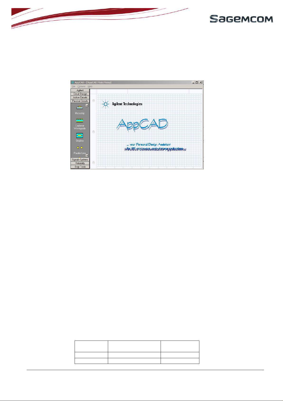
This application notes reminds basics design rules and theirs applications around Sagemcom Hilo module. Some
calculations and length effects can understand with Agilent Appcad tools:
We remind some basics RF principles.
We describe also a method to implement Hilo modules on PCB.
We describe the main issue that designer of electronics system must solved during the design process with Hilo
modules.
2 RF basis
2.1 Wavelength
If we suppose a perfect wire in DC condition: after the first turn on, the current is established. If this wire is not
resistive, we don’t have any voltage drift resulting of ohm low: Everywhere on this line, and referred to the
ground, the voltage is the same.
If we applied an RF signal, instead of DC, the input voltage is continuously changing. This potential can not be
instantly the same everywhere on this line: we are limited to the celerity of the signal, which is close to the celerity
light. Where you are on this line, it is necessary to wait a few times that the potential arrives to you. The potential
over the line can’t be the same everywhere. Thus in RF conditions, any length of wire will introduce some voltage
change and not only due to ohms low. This effect, when it is wanted, is responsible of antenna radiating
properties.
Any length will introduce phase effects. That’s why it is necessary to minimize the connection to ground for all the
components connected to 0 V signal. Otherwise, Hilo PIN physically connected to ground, won’t be electrically at
0V. Depending of amplitude of this issue, it can produce unwanted effects: degradations of transmitting and
receiving performances, reset..
We must compared frequencies used and usual electrics length. Consider the Hilo modules frequency band:
band
EGSM 890-960 32
DCS1800 1710-1880 17
Note d’étude / Technical document :
URD1 - OTL 5635.1– 118 / 72618 ED01
Frequencies for RX and
TX in Mhz
Radio Application Note for Hilo HiloNC modules
Wavelength in
the air (cm)
04 jan 2012 - Page 5 / 36

and PCS1900
UMTS band 1 1922-2167 16
At 1900 Mhz, the wavelength is about 16 cm in the air. These wave lengths will be reduced in the FR4 PCB.
Let’s consider a micro strip line on FR4 PCB with 0,8 mm space between ground and track:
Thus, the quarter wave equal only 22mm for an incoming signal at 1900 Mhz. We recall that in a quarter wave
section, when one side is at 0V, the other side is at the maximum voltage. Thus, few millimeters of conductors can
have electrical drift effect.
Minimize conductor’s length in RF design
Minimize connections length to ground layer
Classics ohm law doesn’t applied to RF design
2.2 Matched load at 50 ohms
In first linear approach, and for best reliability, a generator must be loaded by its conjugate complexes impedance.
In case of internal real impedance, the generator must be loaded by the same impedance value. In RF design we
used the 50ohms value. Hilo modules are designed to work on 50 ohms load. Thus, filters, transmissions lines,
coaxial connectors and antenna must be designed for this value.
For antenna, coaxial connectors and transmission
line, used only 50 ohms impedance
2.3 50 ohms line principle
We have seen that any length of conductor will introduce some voltage phase shift. The module must see a 50
ohms load. But we can not put the antenna directly on the output PIN module. The solution is the matched
transmission line. If this line is loaded with 50 ohms load, the module will see also 50 ohms load at the input line
Note d’étude / Technical document :
URD1 - OTL 5635.1– 118 / 72618 ED01
Radio Application Note for Hilo HiloNC modules
04 jan 2012 - Page 6 / 36

This is an other example to explain that 50 ohms value in transmission line doesn’t refer to ohms low, but to the
characteristic impedance of line : We look at ratio Z=U/I and distributions of currents and voltage in conductors.
A perfect transmission line mustn’t radiate: electric fields and current are locked into the transmission line if
source, load and transmission line are the same impedance. The coaxial cable offers the best results:
Electric field is totally locked into the cylinder. If the line is matched: the input generator impedance, the output
load and the characteristic impedance are equal. Thus, currents on inner and outer conductors, have the same
amplitude, but are opposite in sign: they cancelled themselves.
For antenna output track respect 50 ohms
impedance line design rules
2.4 Microstrip line
Coaxial connector is not the best choice for SMT components assembly. It is not possible to add components in
series or in parallel on this line. The PCB design process is not compatible with this circular structure. For radio
frequency design on PCB, we prefer planar structures. The microstrip line is well designed for PCB design:
As it is mentioned, a ground plan is absolutely needed below all the radio microstrip tracks! This ground
plan will be on the first board layer below the radio layer (top or bottom), excepted in case of a 50 Ω pad (look
spring contact pad, see §3.4.1 ).
Respect carefully micro strip design rules and dimensions
Be sure that resulting dimensions are compatible with PCB
manufacturer tolerance
Note d’étude / Technical document :
URD1 - OTL 5635.1– 118 / 72618 ED01
Radio Application Note for Hilo HiloNC modules
04 jan 2012 - Page 7 / 36
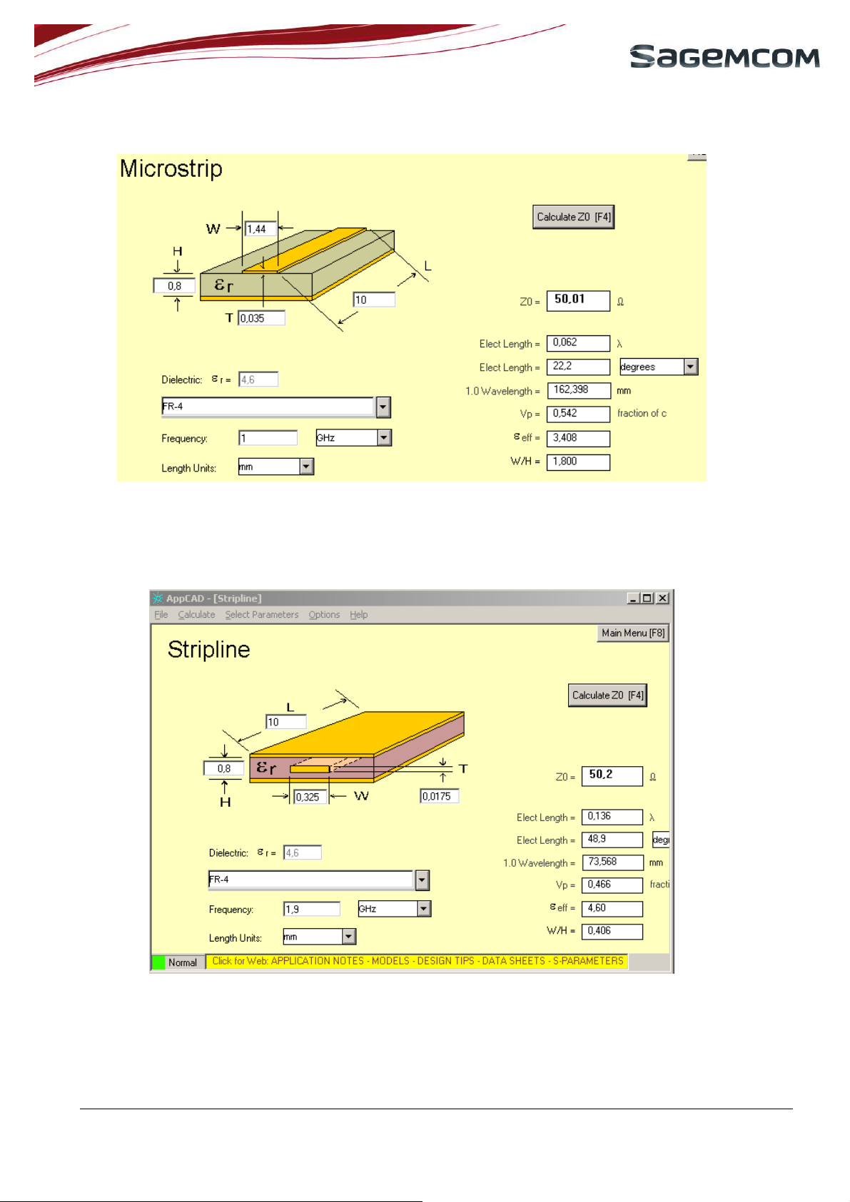
Calculation example:
You must choose your own thickness, and substrate material ( FR4 here). Adjust W to target Z0=50 ohms.
2.5 Stripline design
If the 50 ohms output line doesn’t need any components, you can use the stripline structure:
Anyway the, module antenna port is on the top or bottom side. You need to use via hole to go from external layer
to the internal 50 ohms track.
Note d’étude / Technical document :
URD1 - OTL 5635.1– 118 / 72618 ED01
Radio Application Note for Hilo HiloNC modules
04 jan 2012 - Page 8 / 36

2.6 Coplanar grounded design
A ground plan should be placed on each side of the radio micro strip, on same layer. The distance between the
ground plan and the microstrip (this distance is called G) is important, and we recommend to have a typical value
that can be used is G= 0.8*W.
If G is too low, there will be important power losses in the microstrip due to high coupling between RF signal and
ground. Be sure that width and space dimensions are compatible with your PCB manufacturer.
2.7 Space around PCB line
Resulting from planar geometry, the electric field in a strip line is not perfectly closed into the substrate.
No signals or power supplies should be placed on this ground plan, just below radio microstrip track.
To avoid any coupling effect and transmission mismatch: Don’t place components case, shield or track around
transmission line.
Note d’étude / Technical document :
URD1 - OTL 5635.1– 118 / 72618 ED01
Radio Application Note for Hilo HiloNC modules
04 jan 2012 - Page 9 / 36
Keep some space around micro strip line
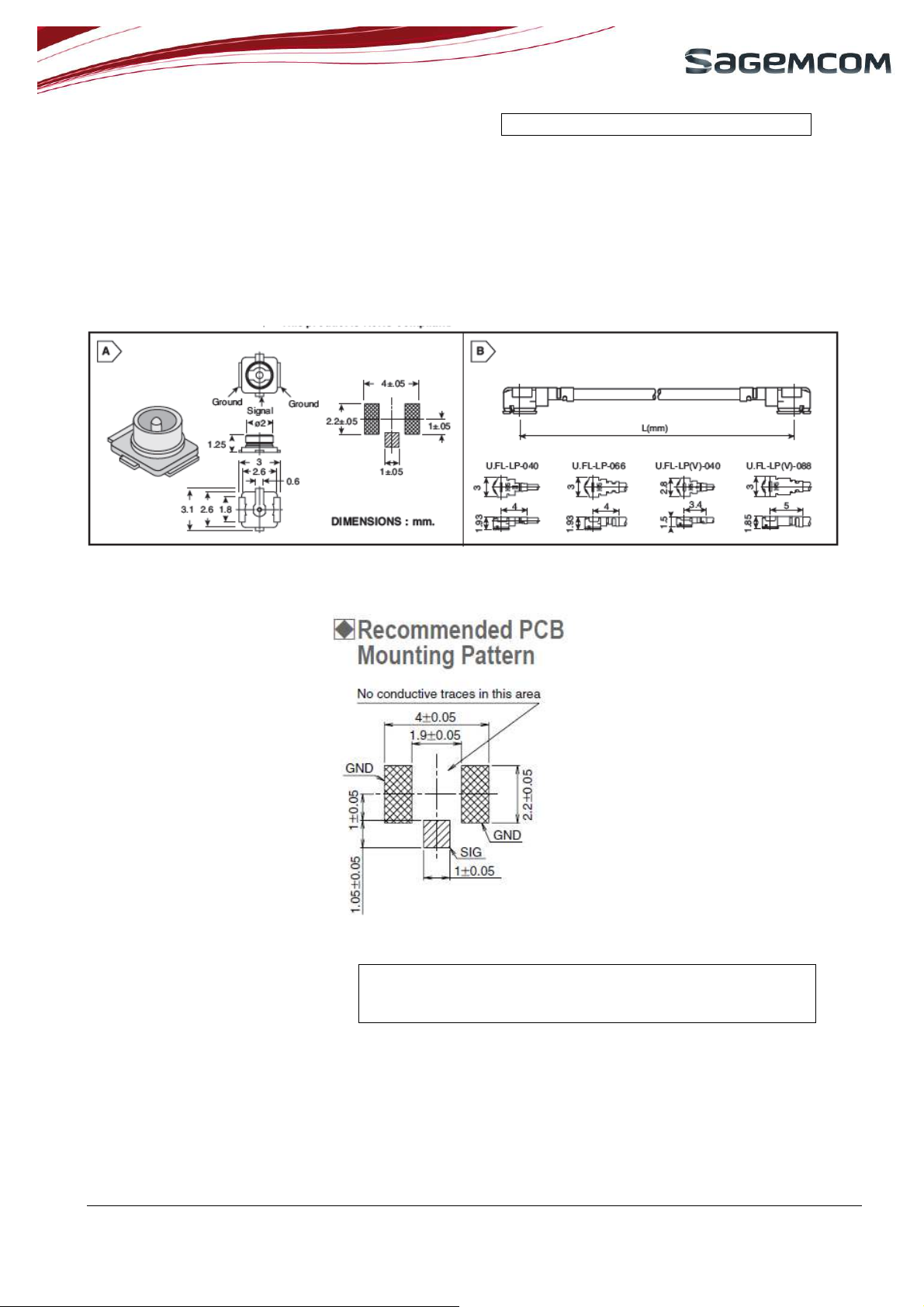
2.8 U.FL coaxial connector
If you are not using the HiloNC version, you can connect a micro-coaxial cable to the module, through the U.FL
connector on Hilo module.
Be careful !! U.FL connector is not designed for a lot of matting-demating operation. You have to take account of
this, during radiated qualification test. A bad connection on “U.FL” type connector can have bad results on
radiated emission during certification process.
For more information about U.FL connectors, look at: http://www.hirose.com/
For the layout, read carefully U.FL the recommended Pattern (here is an example: don’t use values for your
design):
Don’t use any conductive trace under the central pin!!
Follow carefully recommendation for SMT layout
Limits mounting and dismounting operation with U.FL connector
Use new connectors for certification process
3 PCB layout
In RF design, the PCB layout is a part of the design. Due to high integration level, Hilo Module minimize layout
issues and RF knowledge required. But minimal rules must be respected.
Note d’étude / Technical document :
URD1 - OTL 5635.1– 118 / 72618 ED01
Radio Application Note for Hilo HiloNC modules
04 jan 2012 - Page 10 / 36

3.1 Power supply and via to ground
The layout of supply can contributes to final communication behavior. The layout of supply tracks must follow
next rules:
• For VBAT Hilo PIN, it is mandatory to use a track width compatible with burst current in EGSM mode:
1,7A. Remember than any resistive track will introduce a voltage drift.
• Decoupling capacitor positive side must be closed to the VBAT pin. The negative side must be
connected to the ground layer with many via holes.
• It is recommended to use a plain copper under module case connected to ground.
• Via holes must be used for connection between Hilo ground pin and ground layer.
3.2 Hilo case PIN connection
When using Hilo version, you have some pin connections on package. Like demoboard example, it is mandatory
to connect theses pin directly to ground.
Use many via hole to connect this pad to the internal ground layer.
3.3 Decoupling capacitors
A perfect decoupling capacitor must be seen as a short circuit for RF signal. To minimize length of tracks, and
inductive effects, they must be closed to the package and connector. Lower is the capacitor value, closer to the
PIN module it must be.
3.4 Hilo springs connector
On Hilo modules, connectorized versions, you can use springs contacts for antenna connection : “Antenna hot
point” and ‘’ground pad “on next figure:
Note d’étude / Technical document :
URD1 - OTL 5635.1– 118 / 72618 ED01
Radio Application Note for Hilo HiloNC modules
04 jan 2012 - Page 11 / 36
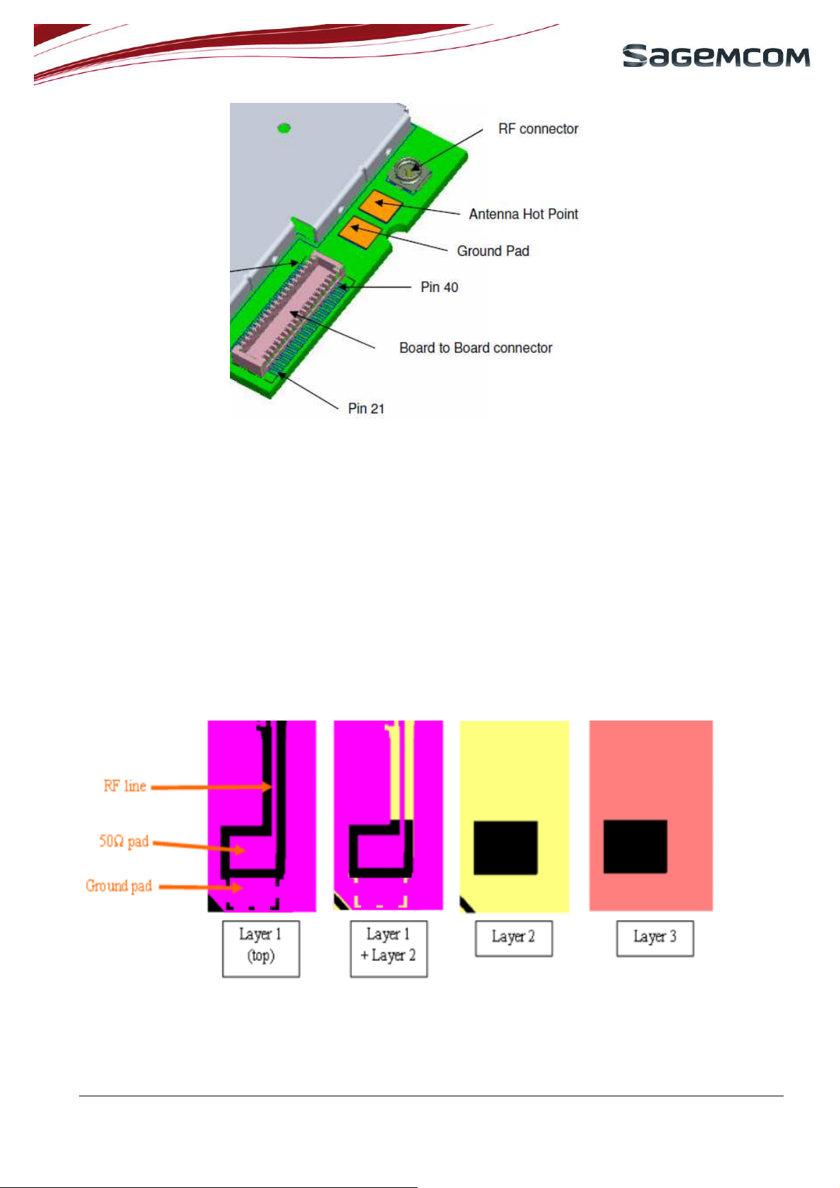
3.4.1 If springs are used
The pad should be 50 Ω, as the RF line connected to it. But since the width of the pad is higher than the width of
the RF line, it means that the distance from the pad to the ground plan below should be higher than the distance
from the RF line to the ground plan below in order to keep the 50 Ω impedance on both.
If we consider the example of RF line given in § 2.4
Dielectric material = FR-4
Microstrip thickness: T = 0.035 mm
Microstrip width: W = 1,44 mm
Distance from the microstrip to the ground plan: H = 0.8mm
Then, when calculating the RF line impedance with these values we obtain 50 Ω. Now, if we consider that the RF
pad has a width of 2.5mm, if we keep H=0.8mm then the impedance of the pad is 33 Ω! To have a 50 Ω pad, H
should become 1.4mm approximately. This explains why we have to remove the ground plan below RF pads on all
layers, until we reach the new H value calculated for the pad only. An example can be seen here:
It is recommended to solder the spring contact on the whole surface instead of only 2 points
Note d’étude / Technical document :
URD1 - OTL 5635.1– 118 / 72618 ED01
Radio Application Note for Hilo HiloNC modules
04 jan 2012 - Page 12 / 36
 Loading...