

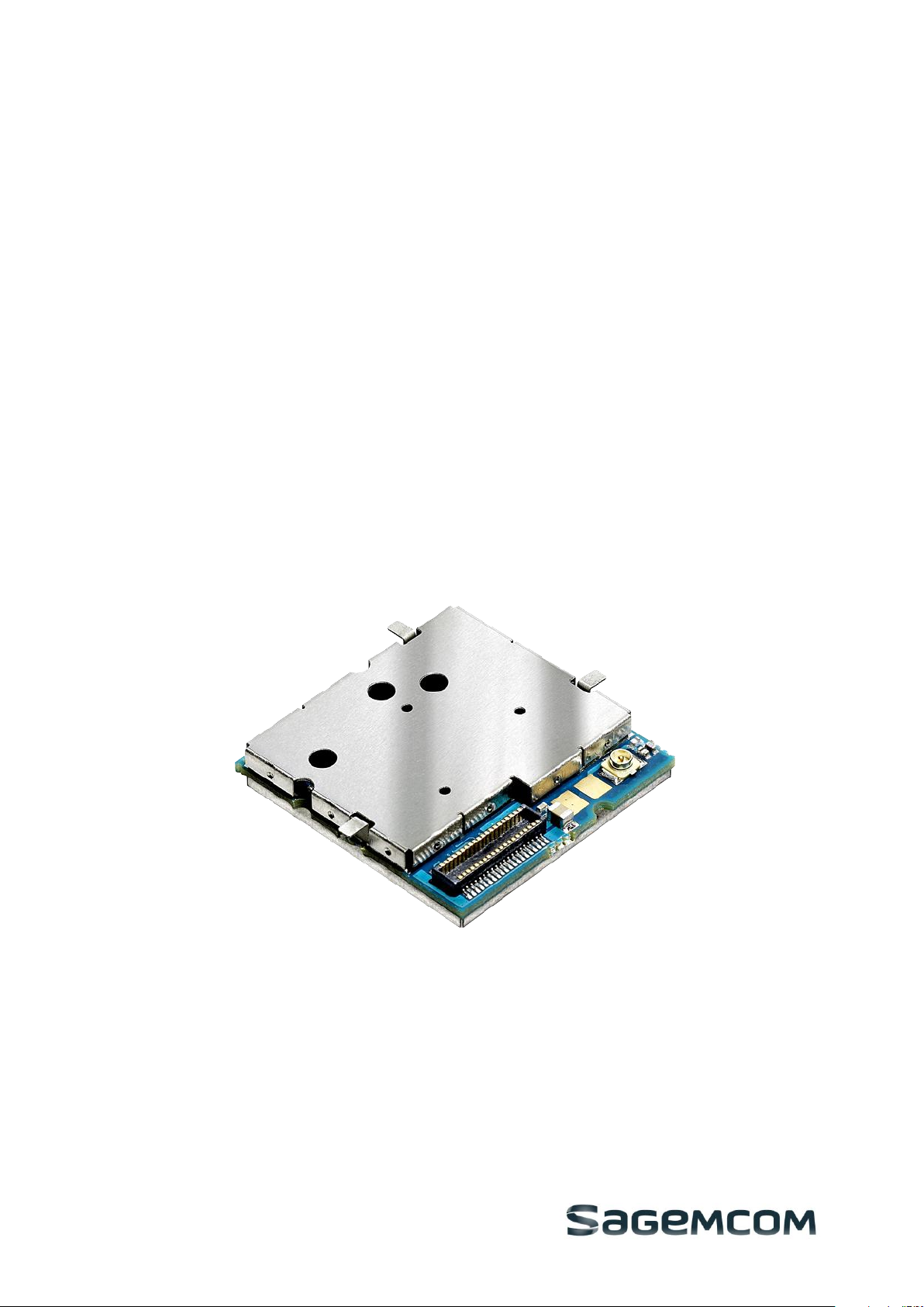
HILO 3G
TECHNICAL SPECIFICATION
~ Freedom of speech
for smart machines ~
FICHE RECAPITULATIVE / SUMMARY SHEET
Ed
1 18/01/2010 URD1– OTL
2 15/03/2010 URD1– OTL
3 17/09/2010 URD1– OTL
4 17/01/2011 URD1 OTL 5696.1-
5 18/03/2011 URD1 OTL 5696.1-
Date
Date
Référence
Reference
5635.2– 001 / 71980
5635.2– 001 / 71980
5635.2– 001 / 71980
004 / 72362 ed 04 -
004 / 72362 ed 05 -
Pages
modifiées
/ Changed
pages
Chapter 2 Block diagram and chapter 8
Update environmental data, mechanical and other
All Changed the document number. Draft watermark
Addition of HiLo3G-850 variant
Creation du document / Document creation
Mechanical updated.
sections
removed
Observations
Comments
Note d’étude / Technical document :
URD1– OTL 5696.1– 004 / 72362 Edition 05
HILO 3G TECHNICAL SPECIFICATION
18/03/2011 - page 2/46

SOMMAIRE / CONTENTS
SOMMAIRE / CONTENTS .................................................................................................................................................3
1. INTRODUCTION......................................................................................................................................................5
1.1 PRODUCT CONCEPT ........................................................................................................................................ 5
1.2 STANDARDS .......................................................................................................................................................5
1.3 TERMS AND ABBREVIATION .........................................................................................................................8
1.4 CONVENTIONS ...................................................................................................................................................9
1.5 PRODUCT FEATURES OVERVIEW ...............................................................................................................9
2. BLOCK DIAGRAM & PINOUT............................................................................................................................ 11
3. FUNCTIONAL DESCRIPTION ............................................................................................................................14
3.1 SIM .......................................................................................................................................................................14
3.1.1 SIM card interface ....................................................................................................................................14
3.1.2 SIM card connection ............................................................................................................................... 14
3.2 AUDIO .................................................................................................................................................................15
3.2.1 ANALOG AUDIO ....................................................................................................................................... 15
3.2.2 DIGITAL AUDIO ........................................................................................................................................15
3.3 PWM ....................................................................................................................................................................16
3.4 DATA ...................................................................................................................................................................16
3.4.1 Data services.............................................................................................................................................16
3.4.2 UART: V24.................................................................................................................................................. 16
3.4.3 USB..............................................................................................................................................................17
3.5 SPARE I/O ..........................................................................................................................................................17
3.6 PWON..................................................................................................................................................................17
3.7 RESET.................................................................................................................................................................18
3.8 ADC ..................................................................................................................................................................... 18
3.9 VBACKUP ..........................................................................................................................................................18
3.10 VGPIO .............................................................................................................................................................18
3.11 POWER SUPPLIES ......................................................................................................................................18
3.12 POWER MANAGEMENT ............................................................................................................................. 19
3.12.1 SLEEP MODES .........................................................................................................................................19
3.12.2 Power supply and power consumption .............................................................................................20
3.12.3 VGPIO..........................................................................................................................................................21
3.12.4 VBACKUP ..................................................................................................................................................21
4. PINOUT ...................................................................................................................................................................22
4.1 I/O CONNECTOR PIN ASSIGNMENTS ........................................................................................................ 22
4.2 POWER DOMAINS AND UNUSED PINS POLICY .....................................................................................24
5. ELECTRICAL SPECIFICATION ......................................................................................................................... 25
5.1 VBAT ...................................................................................................................................................................25
5.2 VBAT WAVEFORM........................................................................................................................................... 26
5.3 VGPIO ................................................................................................................................................................. 27
5.4 VBACKUP ..........................................................................................................................................................27
5.5 VSIM ....................................................................................................................................................................28
5.6 DIGITAL INTERFACE ......................................................................................................................................28
5.7 PWON..................................................................................................................................................................28
5.8 RESET.................................................................................................................................................................29
5.9 SIM .......................................................................................................................................................................29
Note d’étude / Technical document :
URD1– OTL 5696.1– 004 / 72362 Edition 05
HILO 3G TECHNICAL SPECIFICATION
18/03/2011 - page 3/46

5.10 PWM ................................................................................................................................................................ 29
5.11 USB..................................................................................................................................................................29
5.12 ADC .................................................................................................................................................................30
5.13 UART ...............................................................................................................................................................30
5.14 AUDIO SIGNALS...........................................................................................................................................31
5.14.1 Audio Inputs .............................................................................................................................................. 31
5.14.2 Analog Audio Outputs ............................................................................................................................31
5.14.3 Digital Audio..............................................................................................................................................32
5.15 RF SIGNALS .............................................................................................................................................. 33
5.15.1 Load mismatch .........................................................................................................................................33
5.15.2 Input VSWR ...............................................................................................................................................33
5.15.3 Antenna matching network ...................................................................................................................33
6. ENVIRONMENTAL SPECIFICATION................................................................................................................34
6.1 NORMAL TEMPERATURE RANGE..............................................................................................................34
6.2 EXTENDED TEMPERATURE RANGE..........................................................................................................35
6.2.1 Sensitivity .................................................................................................................................................. 35
6.2.2 Transmission characteristics ............................................................................................................... 35
6.2.3 Typical transmission values obtained at extreme temperature................................................... 35
6.3 OUT OF OPERATIONAL RANGE (To be updated)...................................................................................36
7. ESD..........................................................................................................................................................................37
8. MECHANICAL SPECIFICATION........................................................................................................................38
8.1 PHYSICAL DIMENSIONS ................................................................................................................................38
8.2 ASSEMBLY ........................................................................................................................................................40
8.3 TERMINAL ASSIGNMENTS ...........................................................................................................................42
8.3.1 Board to Board connection ................................................................................................................... 42
8.3.2 Antenna connection ................................................................................................................................43
9. ORDERING AND CONTACT INFORMATION .................................................................................................45
9.1 PART NUMBERS ..............................................................................................................................................45
9.2 CONTACT...........................................................................................................................................................45
10. REFERENCE DOCUMENTS...............................................................................................................................46
Note d’étude / Technical document :
URD1– OTL 5696.1– 004 / 72362 Edition 05
HILO 3G TECHNICAL SPECIFICATION
18/03/2011 - page 4/46
1. INTRODUCTION
This document describes the hardware interface of the Sagemcom HiLo 3G M2M module used to connect the
device application and the air interface.
1.1 PRODUCT CONCEPT
The HiLo 3G module is one of the smallest available UMTS/HSDPA module of the market with an industrial
connector. The target application is the Machine to Machine (M2M) market including automotive, AMM
(Automatic Metering Management), tracking system, Alarm, etc. Despite its small size and cost, it has
comprehensive GPRS/EDGE/HSDPA data services.
In addition to its size it has the following outstanding characteristics:
• Automotive temperature range: -40°C to +85°C
• Minimum low power consumption in idle mode: 1.4mA
• High input voltage range: 3.2 V to 4.4 V
• USB High Speed
• Digital Audio PCM
• Form factor compliant with the HiLo module (thickness is higher)
• Pin to pin compliant with HiLo module for the main mandatory signals (Power, Sim, UART)
There are two variants of the HiLo3G module: HiLo3G-900 and HiLo3G-850. Both are quadband for GSM
(GSM850, GSM900, DCS1800, PCS1900) and triple band for UMTS respectively (Band I – 2100 MHz, Band II –
1900 MHz, Band VIII – 900 MHz) for HiLo3G-900 and (Band I – 2100 MHz, Band II – 1900 MHz, Band V –
850 MHz) for HiLo3G-850
As other Sagemcom GSM/GPRS/EDGE modules, it has a full set of AT commands as well as analogue and
Digital audio interface [1].
In addition to the HiLo 3G module a complete development kit can be provided to customers.
1.2 STANDARDS
This product with its evaluation board has been approved to comply with the directives and standards listed
below:
ID
A-Tick Statement
number for HiLo3G-900
HiLo3G-900 VW3HILO3G FCC ID
HiLo3G-850 VW3HILO3G850
HiLo3G-900 2599H-HILO3G IC
Number
Note d’étude / Technical document :
URD1– OTL 5696.1– 004 / 72362 Edition 05
HiLo3G-850 2599H-HILO3G850
CBS11011
HILO 3G TECHNICAL SPECIFICATION
18/03/2011 - page 5/46
EU Directive – only for HiLo3G-900 variant
« Directive of the European Parliament and of the council of 9 March 1999 on radio
99/05/EC
2004/108/EC Directive on electromagnetic compatibility
2006/95/EC
2002/95/EC RoHS Directive
95/94/EC Automotive EMC Directive
Standards of type approval
3GPP TS 51.010-1 « Digital cellular telecommunications system (Phase 2); Mobile Station (MS)
ETSI EN 301 511 « Candidate Harmonized European Standard (Telecommunications series) Global
GCF-CC v3.39.0
Only for HiLo3G-900
variant
PTCRB NAPRD.03
v5.4
ETSI EN 301 489-7 « Candidate Harmonized European Standard (Telecommunications series) Electro
EN 60 950 Safety of information technology equipment
PTCRB/GCF
2G RF/Protocol/ SIM/
Acoustic :
3GPP TS51.010-1
3G RF : TS 34.121-1
3G Protocol:TS 34.123-1
Acoustic: 3GPP TS
26.132
USIM digital:3GPP TS
31.121
USIM analog: ETSI TS
102230
STK: 3GPP TS 51.010-4
USAT:3GPP TS 31.124
equipment and telecommunications terminal equipment and the mutual recognition of
their conformity », in short referred to as R&TTE Directive 1999/5/EC
« Directive on electrical equipment designed for use within certain voltage limits » (Low
Voltage Directive)
conformance specification »
System for Mobile communications (GSM); Harmonized standard for mobile stations
in the GSM 900 and DCS 1800 bands covering essential requirements under article
3.2 of the R&TTE directive (1999/5/EC) (GSM 13.11 version 7.0.1 Release 1998) »
Global Certification Forum - Certification Criteria
PCS Type Certification Review Board
Magnetic Compatibility and Radio spectrum Matters (ERM); Electro Magnetic
Compatibility (EMC) standard for radio equipment and services; Part 7: Specific
conditions for mobile and portable radio and ancillary equipment of digital cellular
radio telecommunications systems (GSM and DCS)»
GCF: GCF-CC V3.39.0
PTCRB: NAPRD03 V5.4
3GPP TS51.010-1: Mobile Station (MS) conformance specification; Part 1:
Conformance specification
TS 34.121-1 : Terminal conformance specification, Radio transmission and reception
(FDD)
TS 34.123-1: User Equipment (UE) conformance specification; Part 1: Protocol
conformance specification
TS 26.132 : Speech and video telephony terminal acoustic test specification
TS 31.121 UICC-terminal interface; Universal Subscriber Identity Module (USIM)
application test specification
ETSI TS 102230. Technical Specification. Smart cards; UICC-Terminal interface;
Physical, electrical and logical test specification
3GPP TS 51.010-4 : Mobile Station (MS) conformance specification; Part 4: Subscriber
Identity Module (SIM) application toolkit conformance test specification
3GPP TS 31.124 : Mobile Equipment (ME) conformance test specification; Universal
Subscriber Interface Module Application Toolkit (USAT) conformance test specification
Note d’étude / Technical document :
URD1– OTL 5696.1– 004 / 72362 Edition 05
HILO 3G TECHNICAL SPECIFICATION
18/03/2011 - page 6/46
Base Stations (BS),
CE – only for HiLo3G-900 variant
RF: 2G EN301511
(refer to PTCRB/GCF
RF report)
RF: 3GEN301908-2
(refer to PTCRB/GCF
RF report)
RF: 3G EN301908-1
EMC: EN301489-1,-7,24
ETSI EN 301 511 Global System for Mobile Communications (GSM); Harmonized EN
for Mobile Stations in the GSM 900 and GSM 1800 Bands Covering Essential
Requirements Under Article 3.2 of the R&TTE Directive (1999/5/EC)
ETSI EN 301 908-2 Electromagnetic compatibility and Radio spectrum Matters (ERM);
Base Stations (BS), Repeaters and User Equipment (UE) for IMT-2000 ThirdGeneration cellular networks; Part 2: Harmonized EN for IMT-2000, CDMA Direct
Spread (UTRA FDD) (UE) covering essential requirements of article 3.2 of the R&TTE
Directive
EN 301908-1
Electromagnetic compatibility and Radio spectrum Matters (ERM) Repeaters and User Equipment (UE) for IMT-2000 Third-Generation cellular networks Part 1: Harmonized EN for IMT-2000, introduction and common requirements, covering
essential requirements of article 3.2 of the R&T
ETSI EN 301 489-1
Electromagnetic compatibility and Radio spectrum Matters (ERM); ElectroMagnetic
Compatibility (EMC) standard for radio equipment and services; Part 1: Common
technical requirements
ETSI EN 301 489-7
ElectroMagnetic Compatibility and Radio Spectrum Matters (ERM); ElectroMagnetic
Compatibility (EMC) Standard for Radio Equipment and Services; Part 7: Specific
Conditions for Mobile and Portable Radio and Ancillary Equipment of Digital Cellular
Radio Telecommunications Systems (GSM and DCS)
ETSI EN 301 489-24
Electromagnetic Compatibility and Radio Spectrum Matters (ERM); ElectroMagnetic
Compatibility (EMC) Standard for Radio Equipment and Services; Part 24: Specific
Conditions for IMT-2000 CDMA Direct Spread (UTRA) for Mobile and Portable (UE)
Radio and Ancillary Equipment
EN 62311:2008
SAR (MPE) : EN62311
Safety: EN60950-1
FCC
RF : FCC Part 22H (850
MHz Band )
FCC Part 24E (for 1900
MHz Band)
EMI: FCC Part 15B Subpart B - Radio frequency devices subpart B – Unintentional Radiators
SAR (MPE) : OET65C
Note d’étude / Technical document :
URD1– OTL 5696.1– 004 / 72362 Edition 05
Assessment of electronic and electrical equipment related to human exposure
restrictions for electromagnetic fields (0 Hz - 300 GHz)
EN60950-1:
Information technology equipment. Safety. General requirements
FCC Part 22 Subpart H: Cellular Radiotelephone Service;
Subpart I: Offshore Radiotelephone Service;
FCC Part 24 E: Personal Communications Service;Subpart E: Broadband PCS.
HILO 3G TECHNICAL SPECIFICATION
18/03/2011 - page 7/46
IC
RF 2G : RSS-132
RF 3G: RSS-133 RSS-133 - 2 GHz Personal Communications Services
EMI: ICES-003 ICES-003: Digital Apparatus
SAR: RSS-102
A-Tick – only for HiLo3G-900 variant
AS/ACIF S042.1
AS/ACIF S042.3
Requirements of quality
IEC 60068-2 Environmental testing
ISO TS 16959 Hilo3G module is manufactured in accordance with ISO TS 16959 in certified factory
RSS-132 - Cellular Telephones Employing New Technologies Operating in the Bands
824-849 MHz and 869-894 MHz
RSS-102 - Radio Frequency Exposure Compliance of Radio communication Apparatus
(All Frequency Bands)
AS/ACIF S042.1: Requirements for connection to an air interface of a
telecommunications network – Part 1
AS/ACIF S042.3: Requirements for connection to an air interface of a
Telecommunications Network - Part 3: GSM Customer Equipment
1.3 TERMS AND ABBREVIATION
ADC Analog to Digital Converter
CODEC Coder-Decoder
CLIP Calling Line Identification Presentation
COLP Connected Line Identification Presentation
CLIR Calling Line Identification Restriction
COLR Connected Line Identification Restriction
CTS Clear To Send
CSD Circuit Switched Data
CS Codec Scheme
DCS Digital Communications System
DSR Data Set Ready
DTR Data Terminal Ready
EDGE Enhanced Data Rate for GSM Evolution
EGSM Enhanced GSM
ENS Enhanced network selection
EONS Enhanced operator name string
ESD Electrostatic Discharge
ETS European Telecommunication Standard
GSM Global System for Mobile communication
GPRS General Packet Radio Services
HSCSD High Speed Circuit Switched Data
HSDPA High Speed Downlink Packet Access
IC Integrated Circuit or Industry Canada (depends on the context)
I/O Input / Output
ISO International Standards Organization
ITU International Telecommunication Union
JTAG Joint Test Action Group
Kbps or kbit/s kilobit per second
LCD Liquid Crystal Display
LED Light Emitting Diode
Mbps or Mbit/s Megabit per second
Note d’étude / Technical document :
URD1– OTL 5696.1– 004 / 72362 Edition 05
HILO 3G TECHNICAL SPECIFICATION
18/03/2011 - page 8/46
PBCCH Packet Broadcast Channel
PCB Printed Circuit Board
PCM Pulse Code Modulation
PCS Personal Communication System
PWM Pulse Width Modulation
RAM Random Access Memory
RF Radio Frequency
RI Ring Indication
RMS Root Mean Square
RTS Ready To Send
RX Reception
SIM Subscriber Identification Module
SMS Short Message Service
TBC To Be Confirmed
TBD To Be Defined
TX Transmission
UART Universal Asynchronous Receiver and Transmitter
UMTS Universal Mobile Telecommunications System
USB Universal Serial Bus
USSD Unstructured Supplementary Service Data
1.4 CONVENTIONS
Throughout this document, DTE (Data Terminal equipment) indicates the equipment which masters and controls
the module device HiLo 3G by sending AT commands via its serial interface.
DCE (Data Communication Equipment) indicates the module device HiLo 3G.
1.5 PRODUCT FEATURES OVERVIEW
Temperature range Normal range: -20°C to +85°C (fully compliant)
Extended range: -40°C to +85°C (fully functional)
Storage: -40°C to +105°C
Weight (in g) 6.6 g (typical)
ESD ESD protection < 2 kV
Physical dimensions 27x27x4.8 mm (typical)
Connection 40 pins connector + 1 RF UFL connector + 1 pair of antenna pad
Power supply 3.2V to 4.4V range, 3.7V nominal
Power consumption* Off mode: 50 µA typical
Registered idle mode:
• WCDMA: 1.3 mA (DRX=9)
• GSM: 1.4 mA (paging rate=9)
Peak Current
• WCDMA: up to 700 mA
• GSM: up to 1.75A
EDGE DATA: 4 Down + 1 Up Class 10
• GSM 850/900: 450mA
• DCS 1800: 350mA
WCDMA: HSDPA: up to 700mA
Battery charge management and
interface
No battery charge management is included.
*
The power consumption is highly dependent on customer’s product design and environment of the module
Note d’étude / Technical document :
URD1– OTL 5696.1– 004 / 72362 Edition 05
HILO 3G TECHNICAL SPECIFICATION
18/03/2011 - page 9/46
Antenna No antenna is included in the module.
Frequency bands HiLo3G-900
• UMTS bands: I (2100 MHz), II (1900 MHz), VIII (900 MHz)
• GSM bands: GSM850, EGSM900, DCS1800, PCS 1900
HiLo3G-850
• UMTS bands: I (2100 MHz), II (1900 MHz), V (850 MHz)
• GSM bands: GSM850, EGSM900, DCS1800, PCS 1900
Voice codec Half Rate, Full Rate, Enhanced Full Rate, Adaptive Multi Rate
GSM class Small MS
Transmit power Class 4 (2W) for GSM850 / EGSM900
Class 1 (1W) for DCS1800 / PCS1900
Class E2 EDGE 900 / 1800
Class 3 for UMTS 900/1900/2100
Supported SIM card 3V and 1.8V SIM cards
SIM slot Signals for the management of the SIM card are provided on 40 pins
connector
PWM Signal for LED, vibrating device and Buzzer management is provided
on the PWM pin
Audio up-link 1 differential input is provided for microphone
Audio down-link 1 differential output is provided for non stereo earphone
Digital audio link Digital audio interface PCM bus is provided. Master mode with 16 bits
and 2048 KHz frequency.
UART interface with flow control Up to 4 Mbit/s for data transmission (no autobauding)
Full flow control signals (+2.9V) are provided on 40 pins connector.
A reference schematic to build the RS232 interface is provided in the
HiLo 3G application note.
USB Supported USB High speed 480Mbps and full speed 12Mbps, with 3
logical Channels
Data services HSDPA, GPRS, EDGE, CSD
Supplementary services
(supported via AT commands)
Power on pin Available
General purpose I/Os pin 3 GPIO + 1 ADC available
GSM release R99
UMTS/WCDMA release R5
GPRS SMG 31bis, Multi slot class 12, class B terminal, PBCCH support, 3
EDGE Multi slot class 12
UMTS/HSDPA Class E2, Voice and Data in parallel for UMTS/HSDPA, 4 logical
HSDPA DL: 3.6 Mbit/s
GSM/DCS certification GCF-CC GCF-CC v3.39.0
PTCRB l NAPRD.03 v5.4
Automatic answer, Internal Phonebook, Caller Line Identification:
CLIP / CLIR / COLP, Call Waiting, Call Hold, Call Forwarding,
Multiparty, Call Barring, Advice of Charge, USSD, CPHS, Fixed
Dialing Number, ENS, EONS.
PDP contexts, CS1 to CS4.
channels
UL: 0.384 Mbit/s
Note d’étude / Technical document :
URD1– OTL 5696.1– 004 / 72362 Edition 05
HILO 3G TECHNICAL SPECIFICATION
18/03/2011 - page 10/46
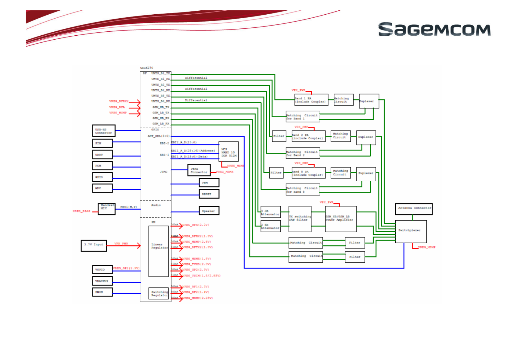
2. BLOCK DIAGRAM & PINOUT
Figure 1: HiLo 3G block diagram
Note d’étude / Technical document :
URD1– OTL 5696.1– 004 / 72362 Edition 05
HILO 3G TECHNICAL SPECIFICATION
18/03/2011 - page 11/46

VBAT Pin 1 Pin 40 VBAT
VBAT Pin 2 Pin 39 VBAT
GND Pin 3 Pin 38 GND
GND Pin 4 Pin 37 GND
USB_DP Pin 5 Pin 36 PCM_CLK
USB_DN Pin 6 Pin 35 PCM_SYNC
VUSB Pin 7 Pin 34 PCM_IN
GPIO3 Pin 8 Pin 33 PCM_OUT
GPIO2 Pin 9 Pin 32 GPIO1
VGPIO Pin 10 Pin 31 PWON
UART_DSR Pin 11 Pin 30 VBACKUP
UART_DCD Pin 12 Pin 29 UART_DTR
UART_TXD Pin 13 Pin 28 UART_RI
UART_CTS Pin 14 Pin 27 UART_RTS
SIM_RST Pin 15 Pin 26 UART_RXD
SIM_CLK Pin 16 Pin 25 SIM_DATA
ADC Pin 17 Pin 24 VSIM
RESET Pin 18 Pin 23 PWM
MIC_N Pin 19 Pin 22 HSET_N
MIC_P Pin 20 Pin 21 HSET_P
Figure 2: HiLo 3G Pinout*
*In blue HiLo 3G pin to pin compliant functions compared to HiLo version.
In red HiLo 3G new feature pins compared to HiLo,
In green HiLo 3G moved functions pins compared to HiLo.
Note d’étude / Technical document :
URD1– OTL 5696.1– 004 / 72362 Edition 05
HILO 3G TECHNICAL SPECIFICATION
18/03/2011 - page 12/46
HiLo3G HiLO
VBAT VBAT Pin 1 Pin 40 VBAT VBAT
VBAT VBAT Pin 2 Pin 39 VBAT VBAT
GND GND Pin 3 Pin 38 GND GND
GND GND Pin 4 Pin 37 GND GND
USB_DP SPI_CLK Pin 5 Pin 36 SPI_SEL PCM_CLK
USB_DN SPI_IRQ Pin 6 Pin 35 SPI_IN PCM_SYNC
VUSB SPI_OUT Pin 7 Pin 34 GPIO5 PCM_IN
GPIO3 GPIO4 Pin 8 Pin 33 GPIO3 PCM_OUT
GPIO2 GPIO2 Pin 9 Pin 32 GPIO1 GPIO1
VGPIO VGPIO Pin 10 Pin 31 PWON PWON
UART_DSR UART_DSR Pin 11 Pin 30 VBACKUP VBACKUP
UART_DCD UART_DCD Pin 12 Pin 29 UART_DTR UART_DTR
UART_TXD UART_TXD Pin 13 Pin 28 UART_RI UART_RI
UART_CTS UART_CTS Pin 14 Pin 27 UART_RTS UART_RTS
SIM_RST SIM_RST Pin 15 Pin 26 UART_RXD UART_RXD
SIM_CLK SIM_CLK Pin 16 Pin 25 SIM_DATA SIM_DATA
ADC PWM0 Pin 17 Pin 24 VSIM VSIM
RESET PWM2 Pin 18 Pin 23 PWM PWM
MIC_N AUX_ADC0 Pin 19 Pin 22 HSET_N HSET_N
MIC_P MIC_P Pin 20 Pin 21 HSET_P HSET_P
HiLO HiLO3G
Figure 3: HiLo 3G & HiLo Pinout Definition
Note d’étude / Technical document :
URD1– OTL 5696.1– 004 / 72362 Edition 05
HILO 3G TECHNICAL SPECIFICATION
18/03/2011 - page 13/46
3. FUNCTIONAL DESCRIPTION
3.1 SIM
3.1.1 SIM card interface
The SIM card interface is compatible with the ISO 7816-3 IC card standard on the issues required by the GSM
11.11 Phase 2+ standard and adapts to 3V and 1.8V SIM card.
To prevent SIM card’s damages, the power supply of the module has to be turned off before any manipulation
on SIM card.
The SIM card interface includes:
• Power supply output (VSIM)
• Bi-direction data signal (SIM_DATA),
• Clock output (SIM_CLK)
• Reset signal (SIM_RST)
Signal Pin N° Description
SIM_RST 15 SIM reset, provided by Base-band processor
SIM_CLK 16 SIM clock, provided by Base-band processor
VSIM 24 SIM supply voltage
SIM_DATA 25 SIM serial data line, input and output
3.1.2 SIM card connection
HiLo 3G
VSIM
SIM_DATA
SIM_RST
SIM_CLK
Figure 4: SIM connection
A reference schematic of the SIM card connection is given in the application note.
SIM card
Note d’étude / Technical document :
URD1– OTL 5696.1– 004 / 72362 Edition 05
HILO 3G TECHNICAL SPECIFICATION
18/03/2011 - page 14/46
3.2 AUDIO
3.2.1 ANALOG AUDIO
The module supports the following voice codec:
• Half-Rate
• Full-Rate
• Enhanced Full Rate
• Adaptive Multi Rate
Signal Pin N° Description
MIC_N 19 Negative polarized input signal for microphone
MIC_P 20 Positive polarized signal for microphone
HSET_P 21 Positive polarized output signal for external speaker
HSET_N 22 Negative polarized output signal for external speaker
It manages an external microphone (MIC_P / MIC_N) in differential mode and an external earphone (32 Ohms
HSET_P/HSET_N) in differential mode.
MIC_P
MIC_N
HSET_P
HSET_N
Figure 5: Audio
To ensure proper operation of such sensitive signal, the audio signals should be isolated by ground on DTE
layout. Characteristics of microphone, speaker and reference schematic are given in the application notes.
HiLo 3G
Base-band
Amplifier+
Filter
3.2.2 DIGITAL AUDIO
The HiLo 3G M2M module features a PCM interface.
The PCM interface is a High speed full duplex interface that can be used to send and receive digital audio data
to external audio ICs.
PCM interface feature includes the following:
• PCM master mode
• Full duplex operation
• 16 bits PCM data word length
• Configurable PCM clock rate up to 2 MHz
Signal Pin N° Description
PCM_CLK 36 PCM clock signal
PCM_SYNC 35 PCM sync signal
PCM_IN 34 PCM data input
PCM_OUT 33 PCM data output
Note d’étude / Technical document :
URD1– OTL 5696.1– 004 / 72362 Edition 05
HILO 3G TECHNICAL SPECIFICATION
18/03/2011 - page 15/46

3.3 PWM
One PWM pin is available on the module. It’s a general purpose PWM which can be used for driving a vibrating
device, keypad backlight or LED. PWM pin can be controlled through AT commands, allowing several periods
and duty cycles. More details are given in the AT commands specification.
Signal Pin N° Description
PWM 23 Pulse Width Modulation
3.4 DATA
3.4.1 Data services
The module supports the following services:
• Data over CSD:
• 2400, 4800, 7200, 9600 and 14400 bit/s
• Transparent and non transparent mode
• V.32 or V.110
• Data over GPRS:
• 3 PDP contexts at the same time
• PBCCH
• Class 12
• CS1 to CS4
• Data over EDGE
• Class 12
• Data over 3G:
• UMTS/HSDPA: Class E2
• HSDPA: 3.6Mbps
• Voice and Data in parallel
• 4 Logical channels
3.4.2 UART: V24
A V24 interface is provided on external pins of the module with the following signals:
• RX/TX
• RTS/CTS
• DSR
• DTR
• DCD
• RI
UART Speed
AT commands and data transfert: up to 4 Mbit/s
Software download: up to 1 Mbit/s
Note d’étude / Technical document :
URD1– OTL 5696.1– 004 / 72362 Edition 05
HILO 3G TECHNICAL SPECIFICATION
18/03/2011 - page 16/46

Signal
UART_DSR 11 UART Data Set Ready
Pin N° Description
UART_DCD
UART_TX 13 UART Transmit
UART_RTS 27 UART Request To Send
UART_RX 26 UART Receive
UART_CTS 14 UART Clear To Send
UART_RI 28 UART Ring Indicator
UART_DTR 29 UART Data Terminal Ready
12 UART Data Carrier Detect
3.4.3 USB
An USB link is available for the AT commands and a trace port.
This interface is compliant with the USB High Speed (480Mbit/s) and USB Full speed (12Mbit/s) specifications.
If the USB feature is not used on the customers design it is however strongly recommended to leave this
interface accessible through tests points for debug purpose.
Signal Pin N° Description
USB_DP 5 USB Data Positive
USB_DN 6 USB Data Negative
VUSB 7 USB Voltage
3.5 SPARE I/O
There are 3 GPIO that can be customized easily from the customer’s application through appropriate AT
commands. And they can be configured as input or output.
Signal Pin N° Description
GPIO1 32 General Purpose Input/Output 1
GPIO2 9 General Purpose Input/Output 2
GPIO3 8 General Purpose Input/Output 3
3.6 PWON
One power input pin is available to start up the module. This pin is low level active with a de-bouncing delay of
100ms.
Signal Pin N° Description
PWON 31 Low level active input signal to power up the module
Note d’étude / Technical document :
URD1– OTL 5696.1– 004 / 72362 Edition 05
HILO 3G TECHNICAL SPECIFICATION
18/03/2011 - page 17/46

3.7 RESET
One reset input pin is available to reset the module in case of undesirable behavior.
Signal Pin N° Description
RESET 18 Low level active input signal to reset the module
3.8 ADC
One ADC input pin is available to measure an external analog voltage through dedicated AT command.
Signal Pin N° Description
ADC 17 Analog to digital converter input
3.9 VBACKUP
One VBackup pin is available to keep supplying the real time clock 32768 Hz in case of main battery loss.
It is used to connect a backup battery coin cell or rechargeable backup battery or super cap.
This pin is an input / output and can manage the charge function of the backup battery
Signal Pin N° Description
VBACKUP 30 Power supply for backup battery
3.10 VGPIO
This Voltage pin is the reference voltage for the internal digital I/O’s it can be used as a power supply and also
as a module power status (ON/OFF). VGPIO is high when the module starts and remains at this level until the
module is OFF.
Signal Pin N° Description
VGPIO 10 Digital Power supply and power up status
3.11 POWER SUPPLIES
Power supplies pins : 4 for the VBAT and 4 for the GND. It is recommended to connect them all, in order to
lower the power signal path serial resistance.
Signal Pin N° Description
VBAT 1,2,39,40 VBAT power input pins
GND 3,4,37,38 Ground pins
Note d’étude / Technical document :
URD1– OTL 5696.1– 004 / 72362 Edition 05
HILO 3G TECHNICAL SPECIFICATION
18/03/2011 - page 18/46

3.12 POWER MANAGEMENT
3.12.1 SLEEP MODES
There are two kinds of sleep mode, the “off mode” and “stand-by” mode. They are described below.
3.12.1.1 Off mode
When the module is in off mode it can not receive any call, it can not receive any AT commands but can be
awaken either by its internal clock using AT+CALA or using PWON signal [2].
To go to this mode use AT+*PSCPOF.
3.12.1.2 Stand-by mode management
There are three stand-by modes management:
• AT+KSLEEP=0
In this mode the sleep state is controlled by the DTR and by the firmware
- DTR = 1† - The module never goes to sleep mode
- DTR = 0 - The module goes to sleep mode when it is ready and can not be awaken with an AT
command. To wake up the module the user must toggle DTR to 1.
Remark: even in this mode it is possible to use DTR signal to go from data to command mode, however
in this case DTR has to be toggled from 1 to 0 then from 0 to 1.
• AT+KSLEEP=1
In this mode the sleep state is only controlled by the firmware.
The module goes to sleep mode when it is ready. The module may be awaken with any character
received on the UART. However to be sure to wake up the module the “0x00” character has to be sent.
The main interest of the AT+KSLEEP=0 mode is to be able to forbid the sleep mode using the DTR signal.
• AT+KSLEEP=2
In this mode the sleep state is never authorized what ever the DTR state.
A detailed description of those modes is given in [3].
†
Here we gives the logical state, '1' means connected to the ground
Note d’étude / Technical document :
URD1– OTL 5696.1– 004 / 72362 Edition 05
HILO 3G TECHNICAL SPECIFICATION
18/03/2011 - page 19/46

3.12.2 Power supply and power consumption
The power supply input of VBAT ranges from 3.2V to 4.4V and 3.7V is nominal.
All measurements in communication mode are done at maximum RF power transmission (PCL max).
Off mode 50 µA 100 µA
Stand-by mode Paging rate 2 – connected to the
network
Stand-by mode Paging rate 5 – connected to the
network
Stand-by mode Paging rate 9 – connected to the
network
CSD mode – in
communication
GPRS when transmitting
GSM900 /
GSM850(PCL=5)
DCS / PCS(PCL=0)
GSM900 / GSM850
data (CS-4 Class 10 4DL,
1UL)
EDGE when transmitting
DCS / PCS
GSM900 / GSM850
data (MCS-9, Class 10,
4DL, 1UL)
DCS / PCS
GPRS stand-by mode –
1 or 2 PDP context are
open
Current consumption during
a burst‡
UMTS Stand-by mode
DRX=6
UMTS Stand-by mode
DRX=9
GSM900 / GSM850 1.95A 1.72A 1.32A
DCS / PCS 0.9A 0.9A 0.9A
All band 2.6 mA 3 mA
All band 1.3mA 1.3 mA 1.5 mA 1.4mA
UMTS data mode
TX: Maximun power
Channel:
B1 : 9613, 9750, 9887
All band 600 600 mA 690 mA 650
B2 : 9263, 9400, 9537
B8 : 2713, 2788, 2862
-20°C 25°C +85°C
Typ. Typ. Max Typ.
2.8mA 2.8 mA 3 mA 3.1mA
1.7mA 1.7 mA 1.9 mA 2.0mA
1.4mA 1.4mA 1.6 mA 1.8mA
260mA
180mA
600mA
520mA
310mA
310mA
260 mA 290 mA 280mA
180 mA 200 mA 200mA
600 mA 750 mA 650mA
520 mA 610 mA 550mA
310 mA 430 mA 330mA
310 mA 340 mA 320mA
The HiLo 3G behavior in GPRS stand-by mode is
similar to GSM stand-by mode. The power
consumption also depends on DRX and on other
network setting (number of adjacent cells, etc.), it is
between 1.4 mA and 2.8 mA.
‡
A burst transmission happens in Standby, communication and GPRS mode. This measurement is performed with a 22 µ F
capacitor on the power supply path required to remove the overshoot.
Note d’étude / Technical document :
URD1– OTL 5696.1– 004 / 72362 Edition 05
HILO 3G TECHNICAL SPECIFICATION
18/03/2011 - page 20/46

Figure 6: typical GPRS burst in the GSM900 frequency band
3.12.3 VGPIO
This +2.8V supply output is available on external pin of the module and can supply +2.9V external components.
The current capability for 2.9V output is:
- 290mA in active mode
3.12.4 VBACKUP
In order to keep the internal Real Time Clock available, a VBACKUP input is present on the module interface.
Depending on the main battery voltage, the internal RTC is supplied by the VBACKUP or by the main power
supply voltage:
RTC supply with external BACKUP present:
• If VBAT < VBACKUP, internal RTC is supplied by VBACKUP.
• If VBAT ≥ VBACKUP, internal RTC is supplied by VBAT.
An internal mechanism of the HiLo 3G module is able to manage the charge of the backup battery. More details
about the battery choice and the charge schematics are given in the application notes.
Note d’étude / Technical document :
URD1– OTL 5696.1– 004 / 72362 Edition 05
HILO 3G TECHNICAL SPECIFICATION
18/03/2011 - page 21/46

4. PINOUT
4.1 I/O CONNECTOR PIN ASSIGNMENTS
Pin N° Pin name IO Type Description
1 VBAT Power supply input +3.7 V power supply (nominal)
2 VBAT Power supply input +3.7 V power supply (nominal)
3 GND Ground GND
4 GND Ground GND
5 USB_DP Digital bi-directional buffer USB DATA
6 USB_DN Digital bi-directional buffer USB DATA
7 VUSB Digital output buffer USB Voltage
8 GPIO3 Digital bi-directional buffer General purpose input/output 3
9 GPIO2 Digital bi-directional buffer General purpose input/output 2
10 VGPIO Power supply output +2.9V power supply output
11 UART_DSR Digital output buffer UART data set ready
12 UART_DCD Digital output buffer UART data carrier detect
13 UART_TX Digital output buffer UART transmit
14 UART_CTS Digital output buffer UART clear to send
15 SIM_RST Digital output buffer SIM reset
16 SIM_CLK Digital output buffer SIM clock
17 ADC Analog input Analog input to digital converter
18 RESET Digital input buffer General Reset input
19 MIC_N Analog input Differential input from microphone
20 MIC_P Analog input Differential input from microphone
21 HSET_P Analog output Differential output to earphone
22 HSET_N Analog output Differential output to earphone
23 PWM Digital output buffer PWM output
24 VSIM Power supply output SIM power supply
25 SIM_DATA Digital bi-directional buffer SIM data
26 UART_RX Digital input buffer UART receive
27 UART_RTS Digital input buffer UART request to send
Note d’étude / Technical document :
URD1– OTL 5696.1– 004 / 72362 Edition 05
HILO 3G TECHNICAL SPECIFICATION
18/03/2011 - page 22/46
28 UART_RI Digital output buffer UART ring indicator
29 UART_DTR Digital input buffer UART data terminal ready
30 VBACKUP Power supply input/output power supply for RTC backup
31 PWON Digital input Module power on signal
32 GPIO1 Digital bi-directional buffer General purpose input/output 1
33 PCM OUT Digital output buffer Digital audio in
34 PCM_IN Digital input buffer Digital audio out
35 PCM_SYNC Digital bi-directional buffer Digital audio sync
36 PCM_CLK Digital bi-directional buffer Digital audio clock
37 GND Ground GND
38 GND Ground GND
39 VBAT Power supply input +3.7V battery power supply (nominal)
40 VBAT Power supply input +3.7V battery power supply (nominal)
The signals which are unused must be left unconnected. If flow control is not used on UART, the signal RTS
must be connected to the signal CTS and the signal DTR must be connected to the signal DSR. For detailed
information please refer to the HiLo 3G module Application Notes document.
Note d’étude / Technical document :
URD1– OTL 5696.1– 004 / 72362 Edition 05
HILO 3G TECHNICAL SPECIFICATION
18/03/2011 - page 23/46

4.2 POWER DOMAINS AND UNUSED PINS POLICY
Connection
HiLo 3G
Pins
Signal Name Function
Power
domain
1 VBATT POWER 3.7V VBATT
2 VBATT POWER 3.7V VBATT
3 GND POWER 0V 0V
4 GND POWER 0V 0V
5 USB_DP
6 USB_DN
7 VUSB
8 GPIO3
USB 2.9V Left Open
USB
USB
2.9V Left Open
2.9V Left Open
GPIO 2.9V Left Open
9 GPIO2 GPIO 2.9V Left Open
10 VGPIO EXT_VDD 2.9V Left Open
11 UART1_DSR UART 2.9V Loop to DTR
12 UART1_DCD UART 2.9V Left Open
13 UART1_TX UART 2.9V TXD
14 UART1_CTS UART 2.9V Loop to RTS
15 SIM_RST SIM 1.8V or 3 V SIM RESET
16 SIM_CLK SIM 1.8V or 3 V SIM CLOCK
17 ADC
18 RESET
19 MIC_N
ADC 2.1V Left Open
RESET 2.9V Left Open
A-AUDIO 1.8V Left Open
20 MIC_P A-AUDIO 1.8V Left Open
21 HSET_P A-AUDIO 3.7V Left Open
22 HSET_N A-AUDIO 3.7V Left Open
23 PWM PWM 2.9V Left Open
24 VSIM SIM 1.8V or 3V VSIM
25 SIM_DATA SIM 1.8V or 3V SIM DATA
26 UART1_RX UART 2.9V RXD
27 UART1_RTS UART 2.9V Loop to CTS
28 UART1_RI UART 2.9V Left Open
29 UART1_DTR UART 2.9V Loop to DSR
30 VBACKUP EXT_VDD 3V Left Open
31 PWON POWER ON 2.9V POWER ON
32 GPIO1 GPIO 2.9V Left Open
33 PCM OUT
34 PCM_IN
35 PCM_SYNC
36 PCM_CLK
D-AUDIO 2.9V Left Open
D-AUDIO
D-AUDIO
D-AUDIO
2.9V Left Open
2.9V Left Open
2.9V Left Open
37 GND POWER 0V 0V
38 GND POWER 0V 0V
39 VBATT POWER 3.7V VBATT
40 VBATT POWER 3.7V VBATT
when not
used /
Mandatory
connected
Note d’étude / Technical document :
URD1– OTL 5696.1– 004 / 72362 Edition 05
HILO 3G TECHNICAL SPECIFICATION
18/03/2011 - page 24/46

VBAT period (ms)
VBAT low duration (us)
VBAT period
VBAT rise time (us)
VBAT fall time (us)
VBAT maximum voltage (V)
VBAT minimum voltage (V)
VBAT drop voltage (mV)
5. ELECTRICAL SPECIFICATION
Five system operating states are defined:
• NO SUPPLY: No power voltage is present.
• BACKUP: Only backup battery is present.
• OFF: Main power voltage is present, backup voltage present or not.
• ACTIVE: Main power voltage is present, backup battery present or not. Internal power supplies are on.
• SLEEP: Main power voltage is present, backup battery present or not. Internal power supplies are in low
power mode.
If not specified, all electrical values are given for the active state at VBAT=3.7V and an operating temperature of
25°C.
5.1 VBAT
The module is supplied through the VBAT signal with the following characteristics:
Parameter Name Min Typ
VbatTe (*) 4.614 4.615 DC
Max
VbatTi (*) 550 -
VbatTr (*) 0 - -
VbatTf (*) 0 - -
VbatMax (*)
VbatMin (*) 3.2 - -
DeltaVbat (*)
Transient voltage (V) 2.9 - Noise level
(Vrms)@100KHz-1MHz
(*): cf. Application Notes for more details.
(**): This value depends on the power supply serial resistor (plus contact and tracks serial resistors)
- - 50mV
- -
- - 300 (**)
4.4
Note d’étude / Technical document :
URD1– OTL 5696.1– 004 / 72362 Edition 05
HILO 3G TECHNICAL SPECIFICATION
18/03/2011 - page 25/46

5.2 VBAT WAVEFORM
VBatMax
DeltaVbat
VbatTe
VbatT
VbatT
VbatTr
VBatMin
This signal shape is due to the drops on Vbat when the radio power amplifier drains the current at the GSM rate
of 217Hz
Figure 7: VBAT voltage waveform
This signal shape is due to the drops on Vbat when the radio power amplifier drains the current at the WCDMA.
Figure 8: VBAT voltage waveform
Note d’étude / Technical document :
URD1– OTL 5696.1– 004 / 72362 Edition 05
HILO 3G TECHNICAL SPECIFICATION
18/03/2011 - page 26/46

5.3 VGPIO
Signal Min Typ Max Remarks
Voltage level(V) 2.75 2.90 3.05 Both active mode and sleep
mode
Current capability active
mode(mA)
- - 290 mA
Current capability sleep
mode(mA)
Line regulation(mV/V) - - 50 Iout = MAX
Rise Time(us) - - 102us Test load capacitor = 2.2uF
- - 290mA 32KHz system clock enable
5.4 VBACKUP
Parameter Min Typ Max Remarks
Voltage level(V) 1.5
3 3.25
Note d’étude / Technical document :
URD1– OTL 5696.1– 004 / 72362 Edition 05
HILO 3G TECHNICAL SPECIFICATION
18/03/2011 - page 27/46
5.5 VSIM
Parameter Min Typ Max Remarks
Output Voltage(V)
2.7 3 3.15 The appropriate output voltage is
auto detected and selected by
software
1.65 1.80 1.95
Output Current(mA) - - 150
Line Regulation(mV/V) - - 50 IOUT = MAX
Powerup Setting Time(us)
- 10 -
from Power down
5.6 DIGITAL INTERFACE
The digital interface has the following characteristics, which includes UART, PCM, PWM and GPIOs.
Parameter Min Typ Max Remarks
Input Current-High(µA) -10 - 10
Input Current-Low(µA) -10 - 10
DC Output Current-
High(mA)
DC Output Current-
Low(mA)
(1)
(1)
Input Voltage-High(V) 2.4
- - 10 Pin driving a "1" with output set at "0"
-10 - - Pin driving a "0" with output set at "1"
Input Voltage-Low(V) - - 0.4
Output Voltage-High(V) 2.7 - -
Output Voltage-Low(V) - - 0.1
(1)
The maximum current for one GPIO is 10mA
5.7 PWON
The PWON signal has the following characteristics:
Parameter Min Ty
Input Voltage-Low(V) -0.3 0 0.3
Input Voltage-High(V) 1.2 1.8 3.3V
Power up Period (ms) from
100 - PWON falling edge
(debouncing)
Max
pe
Note d’étude / Technical document :
URD1– OTL 5696.1– 004 / 72362 Edition 05
HILO 3G TECHNICAL SPECIFICATION
18/03/2011 - page 28/46

5.8 RESET
The RESET signal has the following characteristics:
Parameter Min Type Max
Input Voltage-Low(V) -0.3 0 0.3
Input Voltage-High(V) 1.2 1.8 3.3
Power up Period (ms) from
RESET falling edge
20 - -
5.9 SIM
VL (V) VH (V) Signal
Min Max Min Max
SIM_RST
SIM_CLK
SIM_DATA
Fully compliant to the GSM11.11 and ISO/IEC
7816-3 standards
5.10 PWM
PWM has the following characteristics
Frequency Duty (%) Remarks Signal
Min Max Min Max
PWM 100Hz 400 KHz 0 100
5.11 USB
USB signals have the following characteristics
VL (V) VH (V) Signal
Min Max Min Max
USB_DP 0 0.3 2.8 3.3
USB_DN 0 0.3 2.8 3.3
VUSB 0 0.3 4.9 5.1
Note d’étude / Technical document :
URD1– OTL 5696.1– 004 / 72362 Edition 05
HILO 3G TECHNICAL SPECIFICATION
18/03/2011 - page 29/46

5.12 ADC
The ADC has the following characteristics. A detailed description of the AT command is given in [1].
Parameter Min Typ Max Remarks
ADC Resolution(bits) - 12 -
Number of Inputs - - 1
Input Voltage Range(V) 0 - 2.1
Update rate per channel - - 2.44MHz
Differential Nonlinearity(bits) - 2
Integral Nonlinearity(bits) - 2
Offset Error(mV) - 30 -
Gain Error(mV/LSB) - 2.53 -
Input Resistance (kΩ) - 2 -
Input Capacitance (pF) - - 53
5.13 UART
TXD, RXD, CTS, RTS, DCD, DSR, DTR and RI have the following characteristics:
VL (V) VH (V) Signal
Min Max Min Max
UART_TX -0.3 0.4 2.5 3.3
UART_RX -0.3 0.4 2.5 3.3
UART_RTS -0.3 0.4 2.5 3.3
UART_CTS -0.3 0.4 2.5 3.3
UART_DCD -0.3 0.4 2.5 3.3
UART_DTR -0.3 0.4 2.5 3.3
UART_DSR -0.3 0.4 2.5 3.3
UART_RI -0.3 0.4 2.5 3.3
Note d’étude / Technical document :
URD1– OTL 5696.1– 004 / 72362 Edition 05
HILO 3G TECHNICAL SPECIFICATION
18/03/2011 - page 30/46

5.14 AUDIO SIGNALS
5.14.1 Audio Inputs
The audio inputs contain the following characteristics:
Parameter Min Typ Max Test Conditions
Maximum input range 1.8V With Gain = - 6dB
Nominal reference level 16mV Typical value Gain = + 34dB
Input Micro amplifier gain (dB) -6 + 50
5.14.2 Analog Audio Outputs
The audio outputs contain the following characteristics:
Parameter Min Typ Max Test Conditions
Maximum output range 1.65
Veff
Load resistance (Ω) 25.6 32
Load=32Ω, THD=1%, Output gain = 8 dB
Output amplifier gain (dB) -28 - 8
Note d’étude / Technical document :
URD1– OTL 5696.1– 004 / 72362 Edition 05
HILO 3G TECHNICAL SPECIFICATION
18/03/2011 - page 31/46

5.14.3 Digital Audio
The audio outputs contain the following characteristics
Note d’étude / Technical document :
URD1– OTL 5696.1– 004 / 72362 Edition 05
HILO 3G TECHNICAL SPECIFICATION
18/03/2011 - page 32/46

5.15 RF SIGNALS
5.15.1 Load mismatch
The module accept a VSWR < 20:1 (all phase angles) without damage or permanent degradation
The module accept a VSWR < 12:1 (all phase angles) without any spurious emission > - 30 dBm
5.15.2 Input VSWR
The typical input VSWR is 1.5:1 (max = 1.5:1)
5.15.3 Antenna matching network
A matching network in HiLo 3G is optimized for 50 ohm work load.
To get good performance in application, an additional matching circuit and adjustment for actual antenna is
required. A π-type matching network is recommended in HiLo 3G application note.
Note d’étude / Technical document :
URD1– OTL 5696.1– 004 / 72362 Edition 05
HILO 3G TECHNICAL SPECIFICATION
18/03/2011 - page 33/46

6. ENVIRONMENTAL SPECIFICATION
Parameter
Ambient temperature
Normal range
Ambient temperature
Extended range
Storage temperature -40°C +105°C
Long damp heat
Operating conditions
Short damp heat
Storage and
transportation conditions
Min Max
-20°C +85°C
-40°C +85°C
Tested at +60°C, 95% RH during 504 hours
Tested at +40°C, 95% RH during 96 hours
6.1 NORMAL TEMPERATURE RANGE
ETSI performances are guaranteed by Sagemcom in the range of -20°C to +85°C.
Enhanced sensitivity performance at 25°C is guaranteed as follow:
Frequency band GSM850 EGSM ETSI value
Min sensitivity (dBm) for BER = 2.4% -106 -106 < -102
Frequency band DCS PCS ETSI value
Min sensitivity (dBm) for BER = 2.4% -106 -106 < -100
Frequency band Typical- ETSI value
EDGE (GMSK modulation) -106 <-104
Frequency band Typical ETSI value
UMTS B1 -109 <-106.7
UMTS B2 -108 < -104.7
UMTS B8 -108 < -104.7
Note d’étude / Technical document :
URD1– OTL 5696.1– 004 / 72362 Edition 05
HILO 3G TECHNICAL SPECIFICATION
18/03/2011 - page 34/46

32
50 50 50
3 3 3
6.2 EXTENDED TEMPERATURE RANGE
6.2.1 Sensitivity
Frequency band GSM850 EGSM
Temperature (°C) -40
Typical sensitivity (dBm) -107
Frequency band DCS PCS
Temperature (°C) -40
Typical sensitivity (dBm) -107
Frequency band EDGE
Temperature (°C) -40
Typical sensitivity (dBm) -107
Frequency band UMTS B1 (2100 MHz)
Temperature (°C) -40 +85
Typical sensitivity (dBm) -110 -107 < -106.7
Frequency band UMTS B2 (1900 MHz)
Temperature (°C) -40 +85
Typical sensitivity (dBm) -109 -106 < -104.7
Frequency band UMTS B5 (HiLo3G-850)
Temperature (°C) -40 +85
Typical sensitivity (dBm) TBD TBD < -104.7
Frequency band UMTS B8 (HiLo3G-900)
Temperature (°C) -40 +85
Typical sensitivity (dBm) -109 -107 < -104.7
+85
-105
+85
-104
+85
-105
-40
-107
-40
-107
+85
-105
+85
-104
ETSI value
< -102
ETSI value
< -100
ETSI value
< -102
ETSI value
ETSI value
ETSI value
ETSI value
6.2.2 Transmission characteristics
6.2.3 Typical transmission values obtained at extreme temperature
Frequency band GSM850 EGSM ETSI value
Temperature (°C) -40
Output power - max. PCL (dBm) 32
Frequency error (Hz) 50
Phase error RMS (degree) 3
Note d’étude / Technical document :
URD1– OTL 5696.1– 004 / 72362 Edition 05
+85
31.7
-40
+85
31.7
min max
31.5 35.5
- 90 + 90
- 5°
HILO 3G TECHNICAL SPECIFICATION
18/03/2011 - page 35/46

70 70 70
3 3 3
Frequency band DCS PCS ETSI value
Temperature (°C) -40
Output power - max. PCL (dBm) 29.1
Frequency error (Hz) 70
Phase error RMS (degree) 3
+85
28.1
-40
28.7
+85
27.7
min max
26.5 30.5
-180 180
- 5°
6.3 OUT OF OPERATIONAL RANGE (To be updated)
No operation is guaranteed by Sagemcom out of the extended range. However, it has been observed on
several modules:
Temperature range Comments
-50°C to -40°C and +85°C to 125°C TBD
125°C to 150°C TBD
T = 150°C TBD
T < -50°C and T > 150°C TBD
Note d’étude / Technical document :
URD1– OTL 5696.1– 004 / 72362 Edition 05
HILO 3G TECHNICAL SPECIFICATION
18/03/2011 - page 36/46

7. ESD
Using human body model from JEDEC JESD 22-A114 standard, the HiLo 3G can stand for +/-2kV ESD
on all pins of the 40 points connector and on the RF connector.
Note d’étude / Technical document :
URD1– OTL 5696.1– 004 / 72362 Edition 05
HILO 3G TECHNICAL SPECIFICATION
18/03/2011 - page 37/46

8. MECHANICAL SPECIFICATION
8.1 PHYSICAL DIMENSIONS
Whole size: 27 x 27 x 4.8 mm
Figure 9: HiLo 3G interface
Note d’étude / Technical document :
URD1– OTL 5696.1– 004 / 72362 Edition 05
HILO 3G TECHNICAL SPECIFICATION
18/03/2011 - page 38/46

Note d’étude / Technical document :
URD1– OTL 5696.1– 004 / 72362 Edition 05
Figure 10: HiLo 3G dimensions
HILO 3G TECHNICAL SPECIFICATION
18/03/2011 - page 39/46

8.2 ASSEMBLY
Shield frame is soldered on HiLo 3G PCB; Shield cover is assembled with shield frame and removable.
The recommended solution to fix the HiLo 3G module is to manually solder the three mounting pins on the
motherboard.
The solder pad geometries for the mounting pins are given in
Figure 14.
The assembly description of the module under the mother board is described in Figure 13.
Figure 11: HiLo 3G decomposition
Note d’étude / Technical document :
URD1– OTL 5696.1– 004 / 72362 Edition 05
HILO 3G TECHNICAL SPECIFICATION
18/03/2011 - page 40/46

page 41/46
Figure 12: HiLo 3G Assembly Geometry on mother board
Note d’étude / Technical document :
URD1– OTL 5696.1– 004 / 72362 Edition 05
HILO 3G TECHNICAL SPECIFICATION
18/03/2011 - page 41/46

page 42/46
Figure 13: Spring contact assembly
8.3 TERMINAL ASSIGNMENTS
8.3.1 Board to Board connection
A pair of 40-pin-connector connects HiLo 3G and DTE.
8.3.1.1 HiLo 3G connector
Dimensions and references:
Pins Number Reference
40 MOLEX 53885-0401
Dimension A B C
mm 11.45 9.5 10.55
Figure 14:HiLo 3G connector drawing
Note d’étude / Technical document :
URD1– OTL 5696.1– 004 / 72362 Edition 05
HILO 3G TECHNICAL SPECIFICATION
18/03/2011 - page 42/46

page 43/46
8.3.1.2 Mother board connector
Dimensions and reference of one connector :
Pin Number References
40 MOLEX 54102-0403
The reference of a reel of connectors is MOLEX 54102-0404.
Dimension A B C
mm 12.6 9.5 10.5
Figure 15: Mother board connector drawing
8.3.2 Antenna connection
Two kinds of antenna connection are for client’s selection.
8.3.2.1 Antenna pad
A pair of copper pad on the HiLo 3G PCB could be used for antenna connection with RF spring
8.3.2.2 Antenna connector
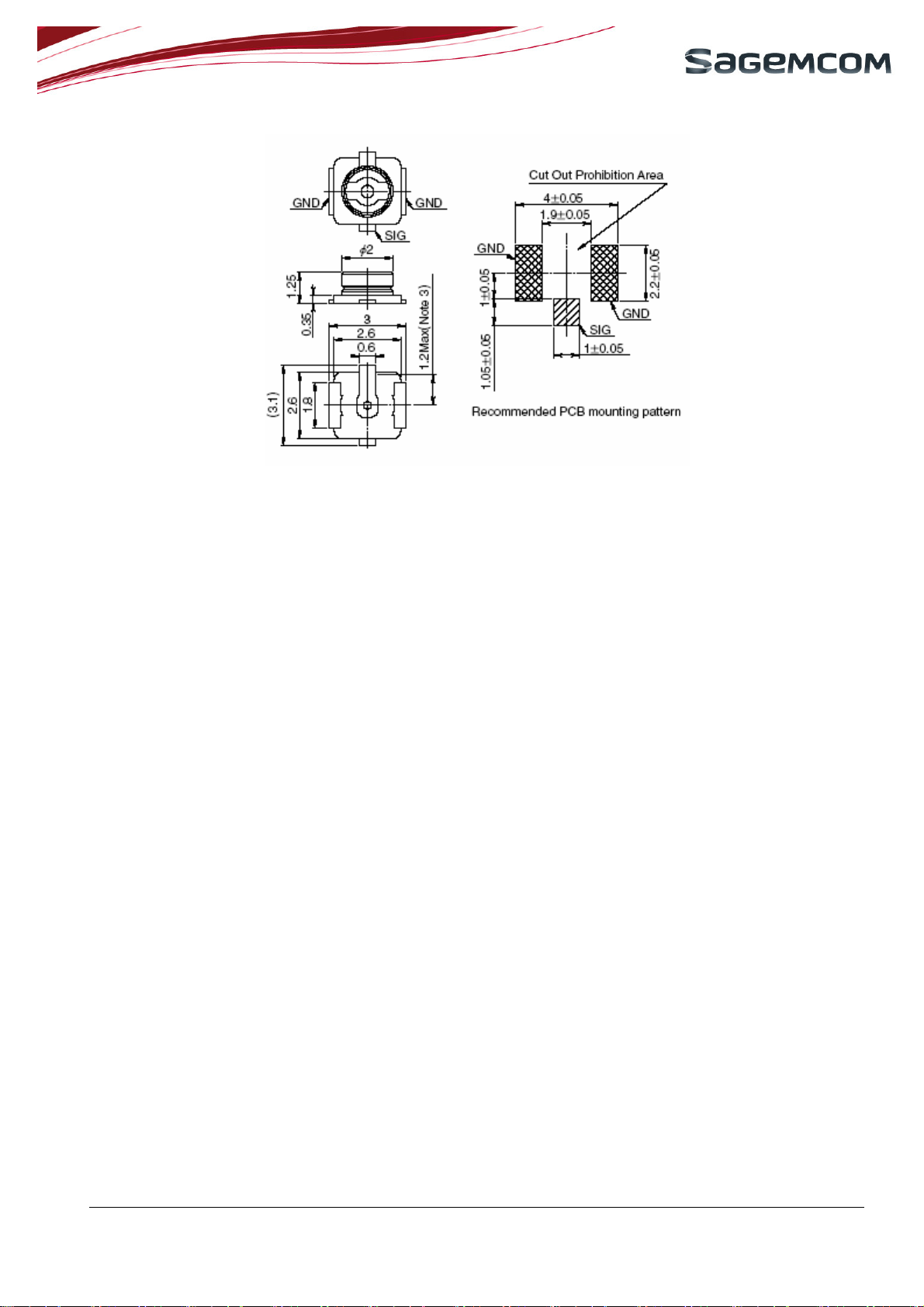
A 50-Ohm RF UFL connector on the HiLo 3G PCB is available for antenna (RF cable) connection.
Reference
HIROSE U.FL-R-SMT-1 (10)
Note d’étude / Technical document :
URD1– OTL 5696.1– 004 / 72362 Edition 05
HILO 3G TECHNICAL SPECIFICATION
18/03/2011 - page 43/46
page 44/46
Figure 16: Antenna connector drawing
Note d’étude / Technical document :
URD1– OTL 5696.1– 004 / 72362 Edition 05
HILO 3G TECHNICAL SPECIFICATION
18/03/2011 - page 44/46

page 45/46
9. ORDERING AND CONTACT INFORMATION
9.1 PART NUMBERS
Modules:
253370547 MODULE HILO3G-900 GENERIC
253412283 MODULE HILO3G-850 GENERIC
Development kits:
253412291 HILO3G-850 DEVELOPMENT KIT
253370550 HILO3G-900 DEVELOPMENT KIT
This reference includes the most recent software and generic parameters
Connector:
189880290 CONN.40C.F.DRT.CMS P=0,5 HCC=2,5(HILO)SP
9.2 CONTACT
Email : wireless-modules@sagem.com
Web : http://www.sagemcom.com/
SAGEMCOM,
Wireless M2M Modules
250, route de l’empereur
92848 Rueil-Malmaison Cedex
FRANCE
Note d’étude / Technical document :
URD1– OTL 5696.1– 004 / 72362 Edition 05
HILO 3G TECHNICAL SPECIFICATION
18/03/2011 - page 45/46

page 46/46
10. REFERENCE DOCUMENTS
[1] URD1 OTL 5696.1 006 72370 - AT Command Set for SAGEMCOM HiLo3G Modules
[2] URD1 OTL 5696.1 003 72361 – HiLo3G application note
[3] Getting started – How to manage DTR
Note d’étude / Technical document :
URD1– OTL 5696.1– 004 / 72362 Edition 05
HILO 3G TECHNICAL SPECIFICATION
18/03/2011 - page 46/46

All rights reserved. The information and specifications included are subject to chan
ge without prior notice. Sagemcom tries to ensure that all information in this document is correct, but does not accept liability for error or
omission. Non contractual document.. All trademarks are registered by their respective owners.
 Loading...