

Page 1

Installation
and
Operation Manual
MODEL X120
INPUT MULTIPLEXER &
CONTROLLER MODULE
MANUAL X120-3000
REVISION 3.6
FEBRUARY 1997
Page 2

Table of Contents
SPECIFICATIONS - MODEL X120 MULTIPLEXER/TERMINATION UNIT................................................................1
1.0 MULTIPLEXER CONTROLLER MODULE X120-1000.........................................................................................2
2.0 DATA FORMAT AND PROTOCOL..........................................................................................................................3
2.1 D
2.2 S
2.3 P
ATA TRANSMISSION FORMAT .....................................................................................................................................3
TATUS FORMAT...........................................................................................................................................................3
ROTOCOL....................................................................................................................................................................3
3.0 SPECIAL FUNCTIONS................................................................................................................................................3
3.1 F
3.2 I
3.3 A
ILTERING .....................................................................................................................................................................3
NPUT CHANNEL TEST...................................................................................................................................................4
LARM SUMMARY........................................................................................................................................................4
4.0 CONFIGURATIONS.....................................................................................................................................................5
4.1 P
4.2 S
ARALLEL CONFIGURATION..........................................................................................................................................5
ERIAL CONFIGURATION...............................................................................................................................................5
5.0 LED INDICATIONS......................................................................................................................................................6
5.1 T
5.2 T
5.3 S
EST ERROR LED (RED) ..............................................................................................................................................6
RANSMIT ERROR LED (RED)......................................................................................................................................6
TATUS/RUN LED (GREEN)..........................................................................................................................................6
6.0 JUMPER SETTINGS....................................................................................................................................................7
6.1 J2, J3, J4, J5.................................................................................................................................................................7
6.2 J6 J
6.3 J7 J
6.4 J8, J9 J
6.5 J10, J11 J
6.6 J12, J13 J
6.7 J14, J15 J
UMPER ....................................................................................................................................................................7
UMPER ....................................................................................................................................................................7
UMPERS.............................................................................................................................................................7
UMPERS.........................................................................................................................................................7
UMPERS.........................................................................................................................................................8
UMPERS.........................................................................................................................................................8
7.0 SWITCH SETTINGS.....................................................................................................................................................8
7.1 SW2-6..........................................................................................................................................................................9
7.2 SW2-7..........................................................................................................................................................................9
7.3 SW2-8..........................................................................................................................................................................9
7.4 SW3-1
TO SW3-8.........................................................................................................................................................9
8.0 INPUT LOGIC MODULES..........................................................................................................................................9
9.0 REFERENCED DRAWINGS.......................................................................................................................................9
10.0 PARTS LISTS................................................................................................................................................................1
X120-1000 C
X120-1001-230 I
X120-1001-125 I
X120-1001-48 I
X120-1001-24 I
X120-GD-24 G
X120-GD-125 G
ONTROLLER MODULE..........................................................................................................................................1
NPUT LOGIC MODULE....................................................................................................................................2
NPUT LOGIC MODULE....................................................................................................................................2
NPUT LOGIC MODULE......................................................................................................................................3
NPUT LOGIC MODULE......................................................................................................................................3
ROUND DETECTOR MODULE............................................................................................................................4
ROUND DETECTOR MODULE..........................................................................................................................4
ii
Page 3

X120-FCPS2424 POWER SUPPLY ............................................................................................................................................5
X120-FCPS12524 P
X120-FCPS125125 P
X120-FCPS24125 P
X120-LPS-24 P
X120-LPS-48 P
X120-LPS-115 P
X120-LPS-125 P
OWER SUPPLY ..........................................................................................................................................6
OWER SUPPLY ........................................................................................................................................6
OWER SUPPLY ..........................................................................................................................................7
OWER SUPPLY..................................................................................................................................................7
OWER SUPPLY..................................................................................................................................................8
OWER SUPPLY................................................................................................................................................9
OWER SUPPLY..............................................................................................................................................10
ii
Page 4

SPECIFICATIONS - MODEL X120 MULTIPLEXER/TERMINATION UNIT
Features
• Monitors up t o 48 switching devices
• Reliable high-speed event transmission
• Interfaces with most plant computers and the Ronan Model X110 Serial Input Visual Annunciator
• Internal relay for self-test and power supply status
• Digital filtering to assure accurate monitoring of status changes
• Up to 32 units may be series connected to monitor up to 1,536 total inputs
• Considerable savings in cable costs by the use of serial transmission
General Description
The Ronan Model X120 Multiplexer/Termination Unit is designed to continuously monitor up to 48 field contacts and/or
solid state switching devices. Any input status change is converted to serial data which can be transferred to a plant computer
or serial input display device, like Ronan’s Model X110 visual annunciator. The input signals are monitored using optoisolated input circuits to provide isolation between input signal voltages and the Model X120 logic circuits. The 48 inputs are
sequentially scanned on a continuous basis.
Input status changes are digitally filtered for a 16 millisecond period before being transmitted over the high speed serial line.
Self-test and watchdog timer circuits, in addition to power supply monitor circuits, are displayed by means of LED indicators.
Loss of a power supply voltage will de-energize the self-test relay.
Up to 32 Model X120 units can be daisy-chained to form a single serial output which monitors the status of up to 1,536 field
contacts or solid state switching devices.
Each Model X120 unit receives 5 VDC power to operate its internal logic. An isolated 125 VDC or 24 VDC voltage source
can be used to power the field contacts. The isolated power source, along with digital filtering, assures maximum noise
immunity for system operation.
Specifications
Input Voltage: X120 Logic: 5 VDC, 24 VDC, 48 VDC, 115 VAC, 125 VDC or 230 VAC ± 10%
Isolated Field Contact: 24 or 125 VDC ± 20%
Power Requireme nts: Isolated: 0.5 A @ 24 VDC plus 0.25 A @ 24 or 125 VDC
Non-isolated: 0.75 A @ 24 VDC
Capacity: 48 inputs
Protocol: Ronan Proprietary
Data Transmission:
Type Distance (Feet) Rate (Baud)
RS422/485 4000 2400
4000 4800
4000 9600
2000 19200
Universal Data Format: per point status change
# Symbol: Start of data string
2 Digits:Termination assembly ID
2 Digits:Point ID
1 Character: O=Open, C=Closed, F=False Alarm (ignore message)
ODH Character: End of data string
Ronan Proprietary Data Format: Contact Factory
Page 1 of 12
Page 5

Output Relay:
• Normally energized, SPST 2 A @ 24 VDC
• Monitors internal logic, all power supplies and optional ground detection
Indicators (LED):
• Power supplies available
• Input test error
• Transmit error
• Run/status indication
• Ground fault condition
Operating Temperature: 0-60°C (32-140°F)
Storage Temperature: -40-85°C (-40-185°F)
Minimum Sustained Data Transfer Ra te: 190 events per second (at 19.2 K baud using Ronan proprietary protocol)
Specifications subject to change without notice.
1.0 MULTIPLEXER CONTROLLER MODULE X120-1000
The primary function of the controller board is to gather “event” data from 48 input channels and relay the
collected information to the Model X110 via RS422/485. This is done by continuous scanning of each of the eight
inputs with U7 (1-OF-8 DECODER/DEMULTIPLEXER). There are 8 outputs from U7 (CS0, CS1, CS2, CS3,
CS4, CS5, CS6, CS7) which are used to scan all the channels and to read the status of SW2 and SW3. The function
and the logical address of each output is shown in Figure 1.
IDENT. LOGIC ADDRESS FUNCTION
CS0 8000H READING DATA FROM CH. 1-8
CS1 8001H READING DATA FROM CH. 9-16
CS2 8002H READING DATA FROM CH. 17-24
CS3 8003H READING DATA FROM CH. 25-32
CS4 8004H READING DATA FROM CH. 32-40
CS5 8005H READING DATA FROM CH. 41-48
CS6 8006H READING DATA FROM SW2 è 1-8
CS7 8007H READING DATA FROM SW3 è 1-8
Figure 1
Each time the controller board scans all the input channels, it stores all the data in the internal memory and makes
filter calculations (refer to filtering section for more information). After filter processing, all the status changes of
inputs are transferred to the transmit buffer and ready to be transmitted. If the old status change of any input has
not been transmitted from the transmit buffer before the status of the same input changes, the controller board
would not register the new status change of that input channel. Therefore the old status of input channels would
not be lost before being transmitted to the X110 system.
Page 2 of 12
Page 6
2.0 DATA FORMAT AND PROTOCOL
All the data from the X120 is transmitted serially via RS232 (P1) to a terminal/printer and RS422/485 (P2) to
X110.
2.1 Data Transmission Format
Baudrate = 1200 / 9600
Number of data bits = 7
Number of stop bits = 1
Parity = Even
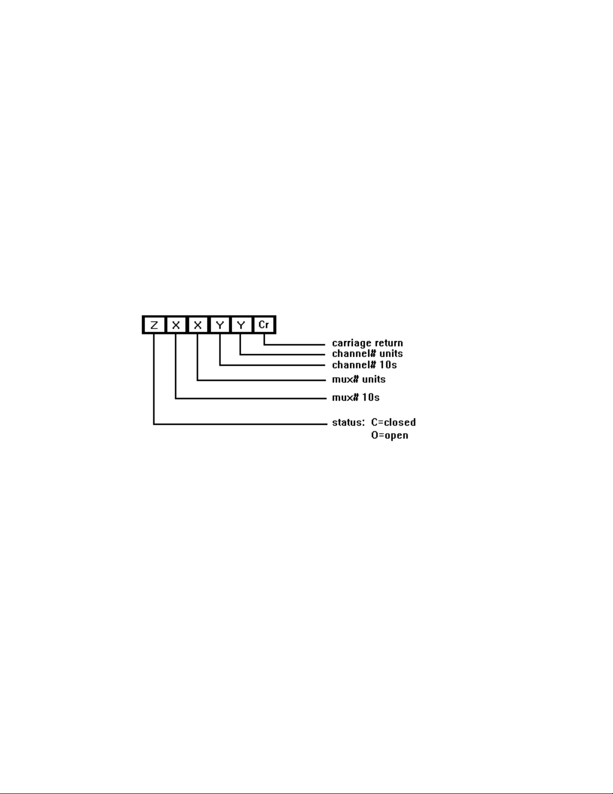
2.2 Status Format
Six bytes of data would be transmitted each time the status of any input channel changes. The formats of
these data bytes are shown below:
2.3 Protocol
The protocol between X120 and X110 is RONAN proprietary and is done to make sure that any status
data transmitted from the X120 would be received by the X110 properly. Each time the X120 transmits a
status change of an input, it will wait for approximately 250ms to receive an ACK (Ctr F) from the X110
which means that the X110 received the data without any error. If after 250ms the ACK is not received,
the same status would be transmitted again up to three times. After the third time, the transmit error LED
would be illuminated and the horn relay would be activated before sending the next status change.
Note: When an ACK is received by the X120, the transmit error LED would be turned off (if it was
on) and the horn relay would be deactivated.
3.0 SPECIAL FUNCTIONS
Along with its event collecting/transmitting tasks, the controller board performs a number of secondary tasks that
are explained in different sections.
3.1 Filtering
Page 3 of 12
Page 7
Before reporting the occurrence of an “event”, the controller board’s program makes “software filter”
calculation. Recall, that a change in the status of a contact must be seen for a specified duration of time
equal to the “time constant value”) before an event is actually declared. The filter calculations are made to
determine when the proper duration of time has expired. The “time constant value” is set to 16ms for all the
input channels.
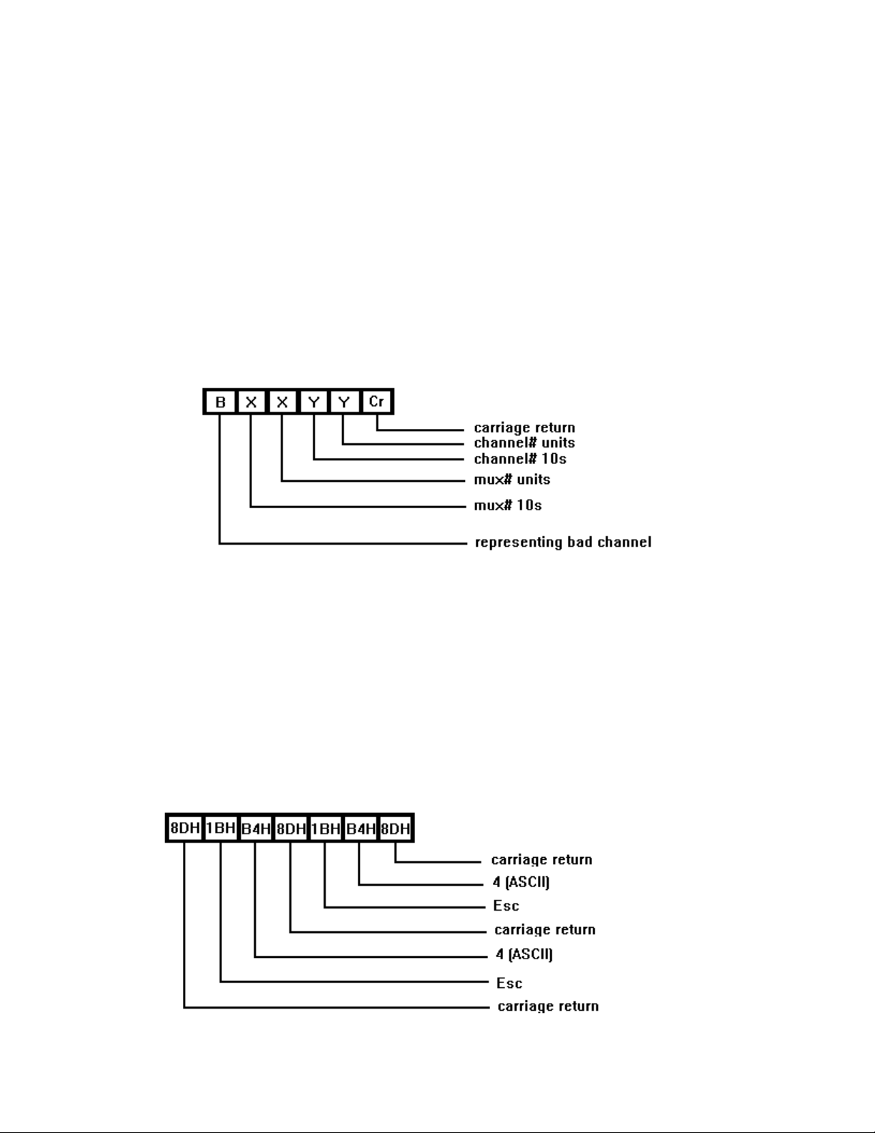
3.2 Input Channel Test
The controller board tests all the 48 input channels of the multiplexer for alarm and return to normal
conditions (only if SW2-7 is set to the ON position) each time it is reset. The test error LED would be
illuminated and the horn relay would be made active if any of the 48 input channels failed to test. This test
is done by using two relays K1 and K2. The K1 relay is used to disconnect the field contact power to all the
inputs. The K2 relay is used to test all the input channels by connecting and disconnecting the field contact
voltage to all the channels and checking all the outputs for proper function. The test error flag would be set
on each channel that was bad and they will be reported before the alarm summary (refer to ALARM
SUMMARY section for more information) with the following format:
The BAD channel report is very useful for troubleshooting input boards. By connecting a terminal to RS232 (P1)
port, all the bad channels (if there is any) would be displayed before the alarm summary each time the X120 is
reset.
Note: The input channel test is valid only if all 48 inputs are set for dry co ntact (B&C jumpers installed).
3.3 Alarm Summary
To update all the annunciator windows with the current status of inputs, Alarm Summary of all the input
channels (open or closed) would be reported if the X120 is reset. To clear all the annunciator windows
before alarm summary, the following data would be sent:
Note: All the data is sent with even parity.
Page 4 of 12
Page 8
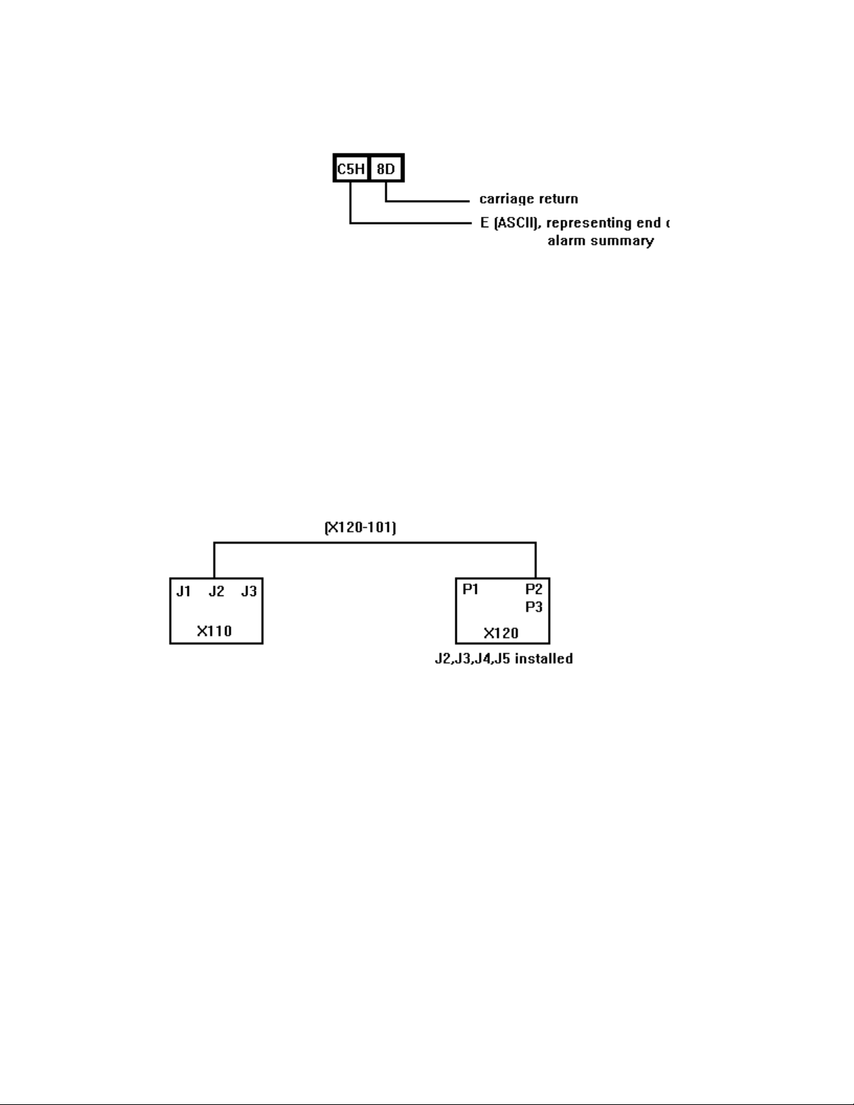
After clearing all the windows, all the bad input channels would be reported (if there is any) only if SW2-7 was set
to the ON position. The alarm summary would be reported next, followed by this data:
4.0 CONFIGURATIONS
The X120 multiplexers can be connected to the X110 system in two different ways (parallel & serial) and J2, J3,
J4, J5 burg jumpers have to be set differently for each X120 in different configurations.
4.1 Parallel Configuration
Only one X120 is connected to the X110(s) in this configuration and J2, J3, J4 and J5 burg jumpers are
used (installed).
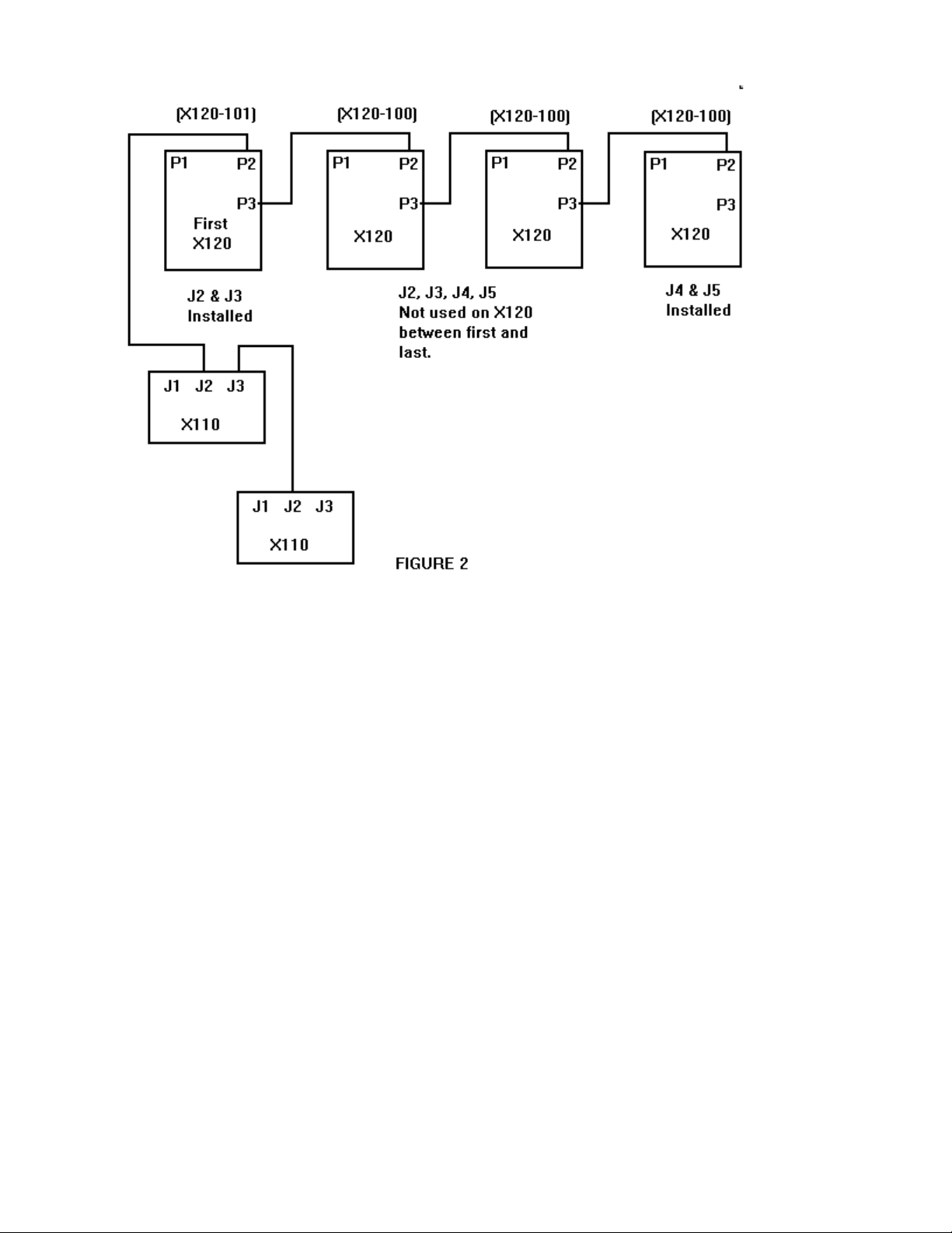
4.2 Serial Configuration
Two to thirty-two X120s can be connected together serially in this configuration. Only J2 & J3 on the
first X120 and J4 & J5 on the last X120 are installed. J2, J3, J4 and J5 should not be installed on any
X120 between first and last.
Figure 2 shows how the X120s are connected serially.
Page 5 of 12
Page 9
5.0 LED INDICATIONS
There are three LEDs on the controller board that indicate the status of the X120s and communication between
X120s and X110s. The operations of these LEDs are explained in the following sections.
5.1 Test Error LED (Red)
Refer to section 3.2.
5.2 Transmit Error LED (Red)
Refer to section 2.3.
5.3 Status/Run LED (Green)
The run/status LED indicates the connection between all the X120 multiplexers. All the run/status LEDs
should be flashing synchronously if connections between all the X120s are okay. The flashing rate
depends on the number of X120 multiplexers connected together and decreases by connecting more
X120(s) in the chain.
Note 1: If any of the X120 multiplexers is transmitting events, the run/status LEDs stop flashing
during the transmission time and stay on or off depending on its state which transmission
started.
Page 6 of 12
Page 10

Note 2: Make sure that all the burg jumpers (J2, J3, J4, J5) are installed properly.
6.0 JUMPER SETTINGS
6.1 J2, J3, J4, J5
Refer to section 4.0.
6.2 J6 Jumper
The DS1232 (U9) provides a watchdog timer function by forcing RST and RST signals to the active state
when the ST input is not simulated for a predetermined time. The time period is set by the TD input to
be 150 ms with TD connected to ground (J6-2&3 installed), 600 ms with TD left unconnected (J6 not
installed), and 1.2 seconds with TD connected to Vcc (J6-1&2 installed).
6.3 J7 Jumper
This jumper is for setting the horn relay contact to normally open or normally closed. The horn relay is
normally energized. To set the horn relay output contact, install (J7-1&2) for normally open and (J7-2&3)
for normally closed.
The factory setting is (J6-1&2 installed)
The factory setting is normally open (J7 -1&2 installed)
6.4 J8, J9 Jumpers
These jumpers are to enable/disable the data transmission to test port (P1). P1 port is used for testing the
X120 boards and can be connected to any terminal with the RS232 port to display the ASCII data
transmitted by the X120 to the X110.
Install J8 & J9 to enable and remove J8 & J9 to disable the data transmission from the X120 to RS232 test
port P1.
Note: The J8 & J9 are installed only on the master controller board to test the system.
6.5 J10, J11 Jumpers
These jumpers are to enable/disable the data reception from RS232 test port (P1) and they are used only
for testing the system.
The factory setting (J8&J9 installed)
The factory setting is (J10&J11 installed)
Note: If you install J10 & J11 for testing the system, disconnect the cable between the X120 and
X110.
Page 7 of 12
Page 11

6.6 J12, J13 Jumpers
Installing a burg jumper on J12 will place in service a 112 ohm line-to-line terminator across the receiver
line (RXD, RXD RTN). If the system is subject to extremely noisy environments, it would be better to
terminate only the receiver side of the communication line by line-to-ground termination on each side of
the receiver line (RXC, RXD RTN). Installing burg jumpers on both J12 and J13 will terminate each side
of the receiver line through 56 ohm to ground .
6.7 J14, J15 Jumpers
Installing a burg jumper on J14 will place in service a 112 ohm line-to-line terminator across the receiver
line (TXC, TXC RTN). Installing burg jumpers on both J14 and J15 will terminate each side of the
transmitter line through 56 ohm to gro und.
7.0 SWITCH SETTINGS
Position 1 to 5 of SW2 are for setting the MUX numbers and they are set as follows:
MUX NUMBER SW2-5 SW2-4 SW2-3 SW2-2 SW2-1
MUX 01 OFF OFF OFF OFF OFF
MUX 02 OFF OFF OFF OFF ON
MUX 03 OFF OFF OFF ON OFF
MUX 04 OFF OFF OFF ON ON
MUX 05 OFF OFF ON OFF OFF
MUX 06 OFF OFF ON OFF ON
MUX 07 OFF OFF ON ON OFF
MUX 08 OFF OFF ON ON ON
MUX 09 OFF ON OFF OFF OFF
MUX 10 OFF ON OFF OFF ON
MUX 11 OFF ON OFF ON OFF
MUX 12 OFF ON OFF ON ON
MUX 13 OFF ON ON OFF OFF
MUX 14 OFF ON ON OFF ON
MUX 15 OFF ON ON ON OFF
MUX 16 OFF ON O N ON ON
MUX 17 ON OFF OFF OFF OFF
MUX 18 ON OFF OFF OFF ON
MUX 19 ON OFF OFF ON OFF
MUX 20 ON OFF OFF ON ON
MUX 21 ON OFF ON OFF OFF
MUX 22 ON OFF ON OFF ON
MUX 23 ON OFF ON ON OFF
MUX 24 ON OFF ON ON ON
MUX 25 ON ON OFF OFF OFF
MUX 26 ON ON OFF OFF ON
MUX 27 ON ON OFF ON OFF
MUX 28 ON ON OFF ON ON
MUX 29 ON ON ON OFF OFF
MUX 30 ON ON ON OFF ON
MUX 31 ON ON ON ON OFF
MUX 32 ON ON ON ON ON
Page 8 of 12
Page 12

7.1 SW2-6
SW2-6 = ON 9600 Baudrate
SW2-6 = OFF 1200 Baudrate
7.2 SW2-7
Position 7 of SW2 is to enable (SW2-7 ON) or disable (SW 2-7 OFF) the input channels tests. Refer to
section 3.2 for more information.
7.3 SW2-8
Position 8 of SW2 is for setting the multiplexer as the master or slave. If there are more than one
multiplexers connected together, set only one of them as the master (SW2-8 ON) and the others as the
slave (SW2-8 OFF).
7.4 SW3-1 to SW3-8
These switches are for spares.
8.0 INPUT LOGIC MODULES
There are 48 filed contact inputs on each input module and each of them is connected to a full wave bridge rectifier
circuit. Two input resistors (R2 & R3) have been added to each circuit for limiting the current and the outputs.
Bridge rectifiers are connected to the opto-isolators which provide both noise immunity and voltage protection for
the internal circuitry. The oto-isolators are then connected to analog delay circuits, which reduce the effects of line
voltage transients. Every 8 outputs from the delay circuits are then connected to an associated line of the octal
buffer which can be read by the controller board.
Each field contact input can be set for dry or live voltage input. Install a burg jumper on position (A) to set the
field contact input to live voltage or install two burg jumpers on positions B & C to set it to dry contact input.
Refer to sheet two of the X120D21 drawing to see how it works.
There are two types of input logic modules, X120-1001 which is equipped with standard input terminals and the
X120-1005 which is equipped with quick-disconnect input terminals. All the other terminals and input circuitry
are the same on both the X120-1001 and X120-1005.
9.0 REFERENCED DRAWINGS
X120-1001 Field Assembly
X120-1000 Multiplexer X120
X120D21 X120-DT Multiplexer Outline & Wiring Information
X120D37 X120-ST Field Multiplexer Assembly
X120C15 X120 to X120 Daisy Chain Cable Assembly
X120C16 X110 to X120 Cable Assembly
X120C36 X120 Extension Cable
These drawings can be found at the end of this manual.
Page 9 of 12
Page 13

10.0 PARTS LISTS
X120-1000 Controller Module
Item Qty Part Number Description I.D.
1 1 X120-1000C PCB
2 2 4310R-101-103 RESISTOR, NETWORK SIP COM 10K RP1,2
3 1 ICL232CPE IC, RECEIVER\TRANS\RS232 U1
4 1 DILB40P-11 IC, SOCKE T\40 U6
5 1 DILB28P-11 IC, SOCKET\28 U11
6 1 80C31 IC, MICROPROCESSOR, CMOS\4KX8 U6
7 1 27C256-2 IC, ROM\PROGRAMMABLE\256K U11
NOTE: THIS PART IS PROGRAMMED BY RONAN TO:
MPBR002 U11 FOR SINGLE AND
X120 010892 MULTIPLE MUX’S
8 1 74HC373 IC, CMOS\LATCH\8\DATA U12
9 1 7437 IC, DRVR\NAND\QUAD\48MA U4
10 1 DS1232 IC, MONITOR\POWER\WATCHDOG TIMER U9
11 2 74HC240N IC, CMOS\INVERTER\TRI-STATE\8 U13,14
12 1 74HC138 IC, CMOS\DECODER\3-8\LINE U7
13 1 SN75174 IC, DRIVER\LINE U3
14 1 SN75175 IC, RECEIVER\LINE U2
15 1 UDN2595A DRIVER, 8 CHANNEL CURRENT SINK U8
16 1 11.059MHZHC-49 XTAL, 11.059M CY1
17 7 104A101C20 CAPACITOR, AXIAL/CER/.1M/100 C8-10,13,16-18
18 1 EP11D1CBE SWITCH, PB\PCB\SPST SW1
19 2 1N4148 DIODE, SIG\75V\400M CR1,2
20 3 T83S11D112-5VDC RELAY, GP\PCB\5DC\DPDT K1-3
21 1 1N270 DIODE, SIGNAL
NOTE: INSTALL CR3 B ACKW ARDS
22 3 RC07GF103J RESISTOR, CF\10K\.25\5 R1-3
23 3 RC07GF511J RESISTOR, CF\510\.25\5 R4-6
24 1 292-0003 CONNECTOR, PCB\EDGE\6
NOTE: INSTALL ON BACK OF THE PCB
25 28 CA36SP100230430 PLUG, STRIP\LINE\36 PINS
NOTE: STRIP 2 OF EACH
26 2 CA36SP100230430 PLUG, STRIP\LINE\36 PINS J6,7
27 2 330R501M05 CAPACITOR, RADIAL\MIC\33P\500 C11,12
28 4 226A100T10 CAPACITOR, AXIAL\TAN\22M\10 C1-4
29 1 745068-7 CONNECTOR, 25 PIN D-TYPE FEMALE P1
30 1 745062-5 CONNECTOR, 15 PIN D-TYPE MALE P3
31 1 745067-5 CONNECTOR, 15 PIN D-TYPE FEMALE P2
32 2 435626-5 SWITCH, DIP\PCB\85W SW2,3
33 2 HLMP-3300 LED, RED\HI\.198
NOTE: LEADS SHOULD BE 4”
34 1 HLMP-3502 LED, GREEN\HI\.198
NOTE: LEADS SHOULD BE 4”
35 1 4308R-102-560 RESISTOR, NETWORK SIP IND 56K RP3
36 1 4308R-102-121 RESISTOR, NETWORK SIP IND RP4
37 6 4-40 X 5/16 PPH SCREW, PHIL\PAN\HD P1-3
CR3
J1
J2-5,8-15
D1,2
D3
Page 14

X120-1001-230 Input Logic Module
Item Qty Part Number Description I.D.
1 1 X120-1001C PCB
2 288 1N4005 DIODE, REC\600\1 CR1-6
3 48 6N139 IC, ISOLATOR\OPTICAL U1-48
4 48 RC07GF105J RESISTOR, CF\1M\.25\5 R1
5 96 RC20GF153J RESISTOR, CF\15K\.5\5 R2,3
6 54 104A101C20 CAPACITOR, AXIAL\CER\.1M\100 C1-54
7 6 4310R-101-103 RESISTOR, NETWORK SIP COM 10K RP1,4,5,8,9,12
8 6 898-3-R100K RESISTOR, NETWORK\DIP\IND\100K RP2,3,6,7,10,11
9 6 74HC240N IC, CMOS\INVERTER\TRI-STATE\8 U49-54
10 2 T83S11D112-5VDC RELAY, GP\PCB\5DC\DPDT K1,2
11 2 1N4148 DIODE, SIG\74V\400M CR7,8
12 192 CA36SP100230430 PLUG, STRIP\LINE\36 PINS
NOTE: STRIP OF 2
13 1 291-0003 CONNECTOR, PCB\EDGE\18 J1
14 4 1731035 TERMINAL BLOCK, PCB 3 POINT TB1-4
15 192 531220-2 SHUNT 2 PIN B,C
16 1 1731022 TERMINAL BLOCK, PCB, 2 POINT TB5
17 48 DILB08P-11T SOCKET, IC U1-48
18 1 V275LA20A VARISTOR, 369\OPR\VOLT V1
19 4 7002922 CONNECTOR TBA,TBB,
20 4 7002922 CONNECTOR TBA, TBB, TBC,
21 2 03JUMPERS JUMPER, .3\.125\22AWG\PVC J1,2
B,C
TBC,TBD
TBD
X120-1001-125 Input Logic Module
Item Qty Part Number Description I.D.
1 NOTE: IDENTIFY BOARD PER X120-1001-125VDC/115VAC
2 1 X120-1001C PCB
3 288 1N4005 DIODE, REC\600\1 CR1-6
4 48 6N139 IC, ISOLATOR\OPTICAL U1-48
5 4 8 RC07GF105J RESISTOR, CF\1M\.25\5 R1
6 96 RC20GF623J RESISTOR, CF\62K\.5\5 R2,3
7 54 104A101C20 CAPACITOR, AXIAL\CER\.1M\100 C1-54
8 6 4310R-101-103 RESISTOR, NETWORK SIP COM 10K RP1,4,5,8,9,12
9 6 898-3-R100K RESISTOR, NETWORK\DIP\IND\100K RP2,3,6,7,10,11
10 6 74HC240N IC, CMOS\INVERTER\TRI-STATE\8 U49-54
11 2 T83S11D112-5VDC RELAY, GP\PCB\5DC\DPDT K1,2
12 2 1N4148 DIODE, SIG\74V\400M CR7,8
13 192 CA36SP100230430 PLUG, STRIP\LINE\36 PINS
B,C
NOTE: STRIP OF 2
14 1 291-0003 CONNECTOR, PCB\EDGE\18 J1
15 4 1731035 TERMINAL BLOCK, PCB 3 POINT TB1-4
16 192 531220-2 SHUNT 2 PIN B,C
17 1 1731022 TERMINAL BLOCK, PCB, 2 POINT TB5
18 48 DILB08P-11T SOCKET, IC U1-48
19 1 V275LA20A VARISTOR, 369\OPR\VOLT V1
20 4 7002922 CONNECTOR TBA,TBB,
TBC,TBD
20 4 7002922 CONNECTOR TBA, TBB,
TBC, TBD
21 2 03JUMPERS JUMPER, .3\.125\22AWG\PVC J1,2
Page 15

X120-1001-48 Input Logic Module
Item Qty Part Number Description I.D.
1 1 X120-1001C PCB
2 288 1N4005 DIODE, REC\600\1 CR1-6
3 48 6N139 IC, ISOLATOR\OPTICAL U1-48
4 4 8 RC07GF105J RESISTOR, CF\1M\.25\5 R1
5 96 RC20GF223J RESISTOR, CF\22K\.5\5 R2,3
6 54 104A101C20 CAPACITOR, AXIAL\CER\.1M\100 C1-54
7 6 4310R-101-103 RESISTOR, NETWORK SIP COM 10K RP1,4,5,8,9,12
8 6 898-3-R100K RESISTOR, NETWORK\DIP\IND\100K RP2,3,6,7,10,11
9 6 74HC240N IC, CMOS\INVERTER\TRI-STATE\8 U49-54
10 2 T83S11D112-5VDC RELAY, GP\PCB\5DC\DPDT K1,2
11 2 1N4148 DIODE, SIG\74V\400M CR7,8
12 192 CA36SP100230430 PLUG, STRIP\LINE\36 PINS
NOTE: STRIP OF 2
13 1 291-0003 CONNECTOR, PCB\EDGE\18 J1
14 4 1731035 TERMINAL BLOCK, PCB 3 POINT TB1-4
15 192 531220-2 SHUNT 2 PIN B,C
16 1 1731022 TERMINAL BLOCK, PCB, 2 POINT TB5
17 48 DILB08P-11T SOCKET, IC U1-48
18 1 V275LA20A VARISTOR, 369\OPR\VOLT V1
19 4 7002922 CONNECTOR TBA,TBB,
20 4 7002922 CONNECTOR TBA, TBB,
20 2 03JUMPERS JUMPER, .3\.125\22AWG\PVC J1,2
B,C
TBC,TBD
TBC, TBD
X120-1001-24 Input Logic Module
Item Qty Part Number Description I.D.
1 1 X120-1001C PCB
2 288 1N4005 DIODE, REC\600\1 CR1-6
3 48 6N139 IC, ISOLATOR\OPTICAL U1-48
4 4 8 RC07GF105J RESISTOR, CF\1M\.25\5 R1
5 96 RC20GF623J RESISTOR, CF\62K\.5\5 R2,3
6 54 104A101C20 CAPACITOR, AXIAL\CER\.1M\100 C1-54
7 6 4310R-101-103 RESISTOR, NETWORK SIP COM 10K RP1,4,5,8,9,12
8 6 898-3-R100K RESISTOR, NETWORK\DIP\IND\100K RP2,3,6,7,10,11
9 6 74HC240N IC, CMOS\INVERTER\TRI-STATE\8 U49-54
10 2 T83S11D112-5VDC RELAY, GP\PCB\5DC\DPDT K1,2
11 2 1N4148 DIODE, SIG\74V\400M CR7,8
12 192 CA36SP100230430 PLUG, STRIP\LINE\36 PINS
NOTE: STRIP OF 2
13 1 291-0003 CONNECTOR, PCB\EDGE\18 J1
14 4 1731035 TERMINAL BLOCK, PCB 3 POINT TB1-4
15 192 531220-2 SHUNT 2 PIN B,C
16 1 1731022 TERMINAL BLOCK, PCB, 2 POINT TB5
17 48 DILB08P-11T SOCKET, IC U1-48
18 1 V275LA20A VARISTOR, 369\OPR\VOLT V1
19 4 7002922 CONNECTOR TBA,TBB,
20 4 7002922 CONNECTOR TBA, TBB,
21 2 03JUMPERS JUMPER, .3\.125\22AWG\PVC J1,2
B,C
TBC,TBD
TBC, TBD
Page 16

X120-GD-24 Ground Detector Module
Item Qty Part Number Description I.D.
1 1 X120-1003A PCB KEY 3-4
2 1 LM393N IC, COMP, LP, LO, DUAL U1
3 1 68WR1MEG POTENTIOMETER, CERAMIC 1M/20 R15
4 3 RC07GF103J RESISTOR, CF, 10K, .25, 5 R16,17,21
5 5 RC07GF105J RESISTOR, CF, 1M, .25, 5 R6,11,13,14,20
6 2 RC07GF115J RESISTOR, CF, 1.1M, .25, 5 R9,12
7 2 RC07GF156J RESISTOR, CF, 15M, .25, 5 R7,8
8 1 RC20GF472J RESISTOR, CF, 4.7K, .5, 5 R3
9 2 RC20GF512J RESISTOR, CF, 5.1K, .5, 5 R1,2
10 2 RC20GF513J RESISTOR, CF, 51K, .5, 5 R4,5
11 2 103A101C10 CAPACITOR, AXIAL, CERAMIC, 0.1M C1,2
12 3 1N4148 DIODE, SIGNAL, 75V, 400M CR1,2,R12
13 1 1N4005 DIODE, REC, 600, 1 CR4
14 2 RC07GF1RJ RESISTOR, CF, 1, .25, 5 CR5,R10
15 1 HLMP3001 LED, RED, STANDARD, .19 POWER
16 2 HLMP1300 LED, RED, STANDARD LED1,2
17 1 2N4249 TRANSISTOR, PNP, 60, 92 Q1
18 1 2N3568 Q2
19 1 T82S11D11424VDCRELAY, GP, PCB, 24DC, DPDT K1
20 1 CP-66 CARD EJECTOR PCB
21 2 22 AWG WIRE, 22 GA BUSS R18,19
X120-GD-125 Ground Detector Module
Item Qty Part Number Description I.D.
1 1 X120-1003A PCB KEY 3-4
2 1 LM393N IC, COMP, LP, LO, DUAL U1
3 1 RC07GF472J RESISTOR, CF, 4.7K, .25, 5
NOTE: STAND A 4.7K OHM RESISTOR ON END &
CONNECT FROMSILKSCREEN SIDE R13 TO SILKSCREEN
SIDE R14.
4 3 RC07GF273J RESISTOR, CF, 27K, .25, 5
NOTE: ON SOLDER SIDE OF PCB, CONNECT A 27KOHM
RESISTOR AT THE FOLLOWING LOCATIONS:
A) SILKSCREEN SIDE R18 TO SILKSCREEN SIDE R14
B) SILKSCREEN SIDE R19 TO SILKSCREEN SIDE R13
5 4 RC07GF103J RESISTOR, CF, 10K, .25, 5
NOTE: ON COMPONENT SIDE OF PCB, CONNECT A
10KOHM RESISTOR FROM SILKSCREEN SIDE R11 TO
OPPOSITE SILKSCREEN SIDE R13.
6 1 RC07GF563J RESISTOR, CF, 56K, .25, 5 R20
7 1 RC07GF105J RESISTOR, CF, 1M, .25, 5
NOTE: ON COMPONENT SIDE ADD A 1 MEGA-OHM
RESISTOR FROM SILKSCREEN SIDE R8 TO OPPOSITE
SILKSCREEN SIDE C2.
8 1 RC07GF106J RESISTOR, CF, 10M, .25, 5 R7
9 1 RC20GF472J RESISTOR, CF, 4.7K, .5, 5 R3
10 2 RC20GF512J RESISTOR, CF, 5.1K, .5, 5 R1,2
11 2 RC20GF393J RESISTOR, CF, 39K, .5, 5
NOTE: ON COMPONENT SIDE OF PCB, ADD A 39KOHM
RESISTOR AT THE FOLLOWING LOCATIONS:
A) SILKSCREEN SIDE R4 TO SILKSCREEN SIDE R18
B) SILKSCREEN SIDE R5 TO SILKSCREEN SIDE R19
R16,17,21
Page 17

12 2 1.5KOHM5W RESISTOR, POWER WW
NOTE: CONNECT RESISTORS AT R18,19 SO THAT TOP OF
RESISTORS ARE LEVEL WITH TOP OF RELAY AT K1
13 2 103A101C10 CAPACITOR, AXIAL, CERAMIC, .01M C1,2
14 2 1N4148 DIODE, SIGNAL, 75V, 400M CR1,2
15 1 1N4005 DIODE, REC, 600, 1 CR4
16 1 1N5359B DIODE, ZENER, 5, 24, 50M CR3
17 2 RC07GF1RJ RESISTOR, CF, 1, .25, 5
NOTE: ON COMPONENT SIDE OF PCB, ADD A ONE OHM
RESISTOR FROM SILKSCREEN SIDE R12 TO OPPOSITE
SILKSCREEN SIDE OF R14.
18 1 HLMP-3001 LED, RED, STANDARD, .19 POWER
19 2 HLMP-1300 LED, RED, STANDARD LED1,2
20 1 2N4249 TRANSISTOR, PNP, 60, 92 Q1
21 1 2N3568-5 TRANSISTOR, NPN, 60 , 92 Q2
22 1 T82S11D11424VDCRELAY, GP, PCB, 24DC, DPDT K1
23 1 CP66 CARD EJECTOR PCB
24 1 1N270 DIODE, SIGNAL
NOTE: ON COMPONENT SIDE ADD A 1N270 DIODE FROM
PIN 4 U1 (ANODE) TO OPPOSITE SILKSCREEN R8
(CATHODE)
25 1 106A350E28 CAPACITOR, AXIAL, ELE, 10M, 35
NOTE: CONNECT CAPACITOR FROM R1,2 SOLDER PAD
(POSITIVE) TO POSITION OPPOSITE OF SILKSCREEN R3
(NEGATIVE). COVER EXPOSED LEADS WITH 22 AWG
TEFLON TUBING. FOR ALL COMPONENT ADDITIONS,
COVER EXPOSED LEADS WITH 22 AWG TEFLON
TUBING.
R18,19
CR5
C3
X120-FCPS2424 Power Supply
Item Qty Part Number Description I.D.
1 1 X120-1002B PCB
2 1 CP66 CARD EJECTOR
3 1 7101P4D9AQE SWITCH, TOGGLE, PCB, SPDT S1
4 1 312.500 FUSE F1
5 2 3529 FUSE HOLDER
6 3 NOT USED COMPONENTS NOT USED C6,J1,R6
7 2 RC07GF100J RESISTOR, CF, 10, .25, 5 R4,5
8 1 RC07GF152J RESISTOR, CF, 1.5K, .25, 5 R1
9 1 RC20GF180J RESISTOR, CF, 18, .5, 5 R2
10 1 02JUMPER JUMPER R7
11 1 RN55C5112F RESISTOR, MF, 51.1K, .125, 1 R3
12 1 101R501M05 CAPACITOR, RAD, MIC, 100P, 500 C3
13 1 104A101C20 CAPACITOR, AXIAL, CER, .1M, 100 C2
14 3 503R501C20 CAPACITOR, RADIAL, CER, .05M, 500 C1,5,7
15 1 156A400E28 CAPACITOR, AXIAL, ELE, 15M, 40 C4
16 2 1N457A DIODE, SIG, 60, 150M D2,3
17 2 1N4937 DIODE, REC, 600, 1 D4,5
18 2 1N4005 DIODE, REC, 600, 1 D7,8
19 1 1N963B DIODE, ZENER, .4, 12, 10M D1
20 2 VN0109N2 FET, N, MOS, 90 TO 39 Q1,2
21 2 2260R HEATSINK ON Q1,2
22 1 CD4047BE IC, BUF, MULTIVIB, LOW, PWR U1
23 1 CD4041UBE IC, BUF, TRUE, COMP, GT, QUAD U2
24 1 HLMP-3300 LED, RED, HI, .198 LED1
Page 18

25 1 T82P11D11424VDCRELAY, GP,PCB,24DC,DPDT K1
26 1 X120B25-6 TRANSFORMER, DC/DC T1
27 2 05JUMPERS JUMPER, .5,.125,22AWG,PVC J2,3
X120-FCPS12524 Power Supply
Item Qty Part Number Description I.D.
1 1 X120-1002B PCB
2 1 CP66 CARD EJECTOR
3 1 7101P4D9AQE SWITCH, TOGGLE, PCB, SPDT S1
4 1 312.150 FUSE, .15A F1
5 2 3529 FUSE HOLDER
6 3 NOT USED COMPONENTS NOT USED C6,J1,R6
7 2 RC07GF100J RESISTOR, CF, 10, .25, 5 R4,5
8 1 UT-2A 50 OHM 5% RESISTOR, PWR/WW/2.5 R2
9 1 NOTE: USE BUSS WIRE FOR R7 .
10 1 RC42GF273J RESISTOR, CF,27K,2,5 R1
11 1 RN55C5112F RESISTOR, MF, 51.1K, .125, 1 R3
12 1 101R501M05 CAPACITOR, RAD, MIC, 100P, 500 C3
13 1 104A101C20 CAPACITOR, AXIAL, CER, .1M, 100 C2
14 3 503R501C20 CAPACITOR, RADIAL, CER, .05M, 500 C1,5,7
15 1 156A400E28 CAPACITOR, AXIAL, ELE, 15M, 40 C4
16 2 1N457A DIODE, SIG, 60, 150M D2,3
17 2 1N4937 DIODE, REC, 600, 1 D4,5
18 2 1N4005 DIODE, REC, 600, 1 D7,8
19 1 1N963B DIODE, ZENER, .4, 12, 10M D1
20 2 VN0350N2 TRANSISTOR Q1,2
21 2 2260R HEATSINK ON Q1,2
22 1 CD4047BE IC, BUF, MULTIVIB, LOW, PWR U1
23 1 CD4041UBE IC, BUF, TRUE, COMP, GT, QUAD U2
24 1 HLMP-3300 LED, RED, HI, .198 LED1
25 1 T82N11D114-24V RELAY K1
26 1 X120B25-3 TRANSFORMER, DC/DC T1
27 2 05JUMPERS JUMPER, .5,.125,22AWG,PVC J2,3
X120-FCPS125125 Power Supply
Item Qty Part Number Description I.D.
1 1 X120-1002B PCB
2 1 CP66 CARD EJECTOR
3 1 7101P4D9AQE SWITCH, TOGGLE, PCB, SPDT S1
4 1 312.150 FUSE .15A F1
5 2 3529 FUSE HOLDER
6 6 NOT USED COMPONENTS NOT USED C6, D6, D9, J1,
R6, VR1
7 2 RC07GF100J RESISTOR, CF, 10, .25, 5 R4,5
8 1 UT-2A 50 OHM 5% RESISTOR, PWR,WW,2.5 R2
9 1 UT-2A 7KOHM 5% RESISTOR, PWR,WW,2.5 R7
10 1 RC42GF273J RESISTOR, CF,27K,2,5 R1
11 1 RN55C5112F RESISTOR, MF, 51.1K, .125, 1 R3
12 1 101R501M05 CAPACITOR, RAD, MIC, 100P, 500 C3
13 1 104A101C20 CAPACITOR, AXIAL, CER, .1M, 100 C2
14 3 503R501C20 CAPACITOR, RADIAL, CER, .05M, 500 C1,5,7
15 1 475A251E28 CAPACITOR, AXIAL, ELE, 4.7M,250 C4
16 2 1N457A DIODE, SIG, 60, 150M D2,3
Page 19

17 2 1N4937 DIODE, REC, 600, 1 D4,5
18 2 1N4005 DIODE, REC, 600, 1 D7,8
19 1 1N963B DIODE, ZENER, .4, 12, 10M D1
20 2 VN0350N2 TRANSISTOR Q1,2
21 2 0771786N PAD, TRANSISTOR Q1,2
22 2 2260R HEATSINK USE ON Q1,2
23 1 CD4047BE IC, BUF/MULTIVIB/LOW/PWR U1
24 1 CD4041UBE IC, BUF/COMP/GT/QUAD U2
25 1 HLMP-3300 LED, RED/HI/.198 LED1
26 1 T82N11D114-48 RELAY K1
27 1 X120B25-2 TRANSFORMER, DC/DC T1
28 2 05JUMPERS JUMPER, .5/.125/22AWG/PVC J2,3
X120-FCPS24125 Power Supply
Item Qty Part Number Description I.D.
1 1 X120-1002B PCB
2 1 CP66 CARD EJECTOR
3 1 7101P4D9AQE SWITCH, TOGGLE, PCB, SPDT S1
4 1 312.001 FUSE 1A F1
5 2 3529 FUSE HOLDER
6 3 NOT USED COMPONENTS NOT USED C6,J1,R6
7 2 RC07GF100J RESISTOR, CF, 10, .25, 5 R4,5
8 1 RC07GF152J RESISTOR, 1/4W, 5%, 1.5K R1
91 JUMPER R2
10 1 UT2A-7K RESISTOR, 2W, 5%, 7K R7
11 1 RN55C5112F RESISTOR, MF, 51.1K, .125, 1 R3
12 1 101R501M05 CAPACITOR, RAD, MIC, 100P, 500 C3
13 1 104A101C20 CAPACITOR, AXIAL, CER, .1M, 100 C2
14 3 503R501C20 CAPACITOR, RADIAL, CER, .05M, 500 C1,5,7
15 1 475A251E28 CAPACITOR, AXIAL, ELE, 4.7M,250 C4
16 2 1N457A DIODE, SIG, 60, 150M D2,3
17 2 1N4937 DIODE, REC, 600, 1 D4,5
18 2 1N4005 DIODE, REC, 600, 1 D7,8
19 1 1N963B DIODE, ZENER, .4, 12, 10M D1
20 2 RFL4N12 V-MOS FET Q1,2
21 2 2260R HEATSINK USE ON Q1,2
22 1 CD4047BE IC, BUF/MULTIVIB/LOW/PWR U1
23 1 CD4041UBE IC, BUF/COMP/GT/QUAD U2
24 1 HLMP-3300 LED, RED/HI/.198 LED1
25 1 T85N11D114-48 or
G5V-2-DC48
26 1 X120B25-5 TRANSFORMER, DC/DC T1
27 2 05JUMPERS JUMPER, .5/.125/22AWG/PVC J2,3
RELAY K1
X120-LPS-24 Power Supply
Item Qty Part Number Description I.D.
1 1 X120-1002B PCB
2 1 CP66 CARD EJECTOR
3 1 7101P4D9AQE SWITCH, TOGGLE, PCB, SPDT S1
4 1 312.500 FUSE F1
5 2 3529 FUSE HOLDER
6 1 RC07GF471J RESISTOR, CF,470,.25,5 R6
Page 20

7 2 RC07GF102J RESISTOR, CF,1K,.25,5 R4,5
8 1 RC07GF152J RESISTOR, 1/4W, 5%, 1.5K R1
9 1 7200-25 INDUCTOR R2
10 1 RC42GF820J RESISTOR, CF,82,2,5 R7
11 1 RN55C5112F RESISTOR, MF, 51.1K, .125, 1 R3
12 1 101R501M05 CAPACITOR, RAD, MIC, 100P, 500 C3
13 2 105R500C20 CAPACITOR, RAD,CERAMIC,1M C1,5
14 1 104A101C20 CAPACITOR, AXIAL,CERAMIC,.1M,100 C2
15 1 503R501C20 CAPACITOR, RAD,CER,0.5M,500 C7
16 1 685R350T10 CAPACITOR, RAD,TAN,6.8M,35 C6
17 1 157A250E28 CAPACITOR, AXIAL,ELE,150M,25 C4
18 2 1N457A DIODE, SIG,60,150M D2,3
19 2 1N4937 DIODE, REC,600,1 D4,5
20 2 1N4005 DIODE, REC,600,1 D6,7
21 1 1N963B DIODE, ZENER,.4,12,10M D1
22 1 MBR160 DIODE, SCHOTTKY D9
23 2 RFL4N12 TRANSISTOR Q1,2
24 2 2260R HEATSINK ON Q1,2
25 1 CD4047B IC, BUF,MULTIVIB,LOW,PWR U1
26 1 CD4041UBE IC, BUF,TRUE,COMP,GT,QUAD U2
27 1 LM7805CT VOLTAGE REGULATOR 5V TO –220 REG1
28 1 HLMP-3300 LED, RED,HI,.198 LED1
29 1 RY-6WZ-K or
T82S11D114-05 or
G5V-2-DC6
30 1 X120B25-4 TRANSFORMER, DC/DC T1
31 2 05JUMPERS JUMPER, .5,.125,22AWG,PVC J1,3
32 1 6072B HEATSINK
33 1 0440X0086PHPHMSSCREW, 4-40X1/4 PHIL,PAN,MS FOR REG1
RELAY K1
34 1 4-40 SM PATTERN NUT, SMALL PATTERN FOR REG1
35 1 4-INT-L/W WASHER, INTE RNAL LOCK FOR REG1
X120-LPS-48 Power Supply
Item Qty Part Number Description I.D.
1 1 X120-1002B PCB
2 1 CP66 CARD EJECTOR
3 1 7101P4D9AQE SWITCH, TOGGLE, PCB, SPDT S1
4 1 312.500 FUSE F1
5 2 3529 FUSE HOLDER
6 1 RC07GF471J RESISTOR, CF,470,.25,5 R6
7 2 RC07GF100J RESISTOR, CF,10,.25,5 R4,5
8 1 UT-2A 20 OHM 5% RESISTOR, PWR,WW,2.5 R2
9 1 RC42GF820J RESISTOR, CF,82,2,5 R7
10 1 RC32GF392J RESISTOR, CF,3.9K,1,5 R1
11 1 RN55C5112F RESISTOR, MF,51.1K,.125,1 R3
12 1 101R501M05 CAPACITOR, RAD,MIC,100P,500 C3
13 1 105R500C20 CAPACITOR, RAD,CERAMIC,1M C5
14 1 104A101C20 CAPACITOR, AXIAL,CER,.1M,100 C2
15 1 503R501C20 CAPACITOR, RAD,CER,0.5M,500 C7
16 1 685R350T10 CAPACITOR, RAD,TAN,6.8M,35 C6
17 1 157A250E28 CAPACITOR, AXIAL,ELE,150M,25 C4
18 1 503R501C20 CAPACITOR, RADIAL,CER,.05M,500 C1
19 2 1N457A DIODE, SIG,60,150M D2,3
Page 21

20 2 1N4937 DIODE, REC,600,1 D4,5
21 2 1N4005 DIODE, REC,600,1 D6,7
22 1 1N963B DIODE, ZNR,.4,12,10M D1
23 1 MBR160 DIODE, SCHOTTKY D9
24 2 VN0340N2 FET, N,MOS,400 TO 39 Q1,2
25 2 2260R HEATSINK ON Q1,2
26 1 CD4047B IC, BUF,MULTIVIB,LOW,PWR U1
27 1 CD4041UBE IC, BUF,TRUE,COMP,GT,QUAD U2
28 1 LM340AT-5.0 TRANSISTOR, REG TO –220 REG1
29 1 HLMP-3300 LED, RED,HI,.198 LED1
30 1 RY-6WZ-K RELAY K1
31 1 X120B25-7 TRANSFORMER, DC/DC T1
32 2 05JUMPERS JUMPER, .5,.125,22AWG,PVC J1,3
33 1 6072B HEATSINK
34 1 0440X0086PHPHMSSCREW, 4-40X1/4 PHIL/PAN/MS FOR REG1
35 1 4-40 SM PATTERN NUT, SMALL PATTERN FOR REG1
36 1 4-INT-L/W WASHER, INTE RNAL LOCK FOR REG1
X120-LPS-115 Power Supply
Item Qty Part Number Description I.D.
1 1 X120-1006B PCB
2 1 05JUMPERS JUMPER, .5/.125/22AWG/PVC J7
3 2 NOT USED COMPONENTS NOT USED J4,8
4 1 RC07GF220J RESISTOR, CF/22/.25/5 R4
5 1 RC07GF271J RESISTOR, CF/270/.25/5 R3
6 1 RC07GF471J RESISTOR, CF,470,.25,5 R1
7 1 RN55C9530F RESISTOR, MF/953/.125/1 R2
8 6 1N4005 DIODE, REC/600/1 D1-6
9 2 1N5817 DIODE, REC/20/1
NOTE: SEE DRAWING X120B148 FOR D5 INSTALLATION.
10 1 HLMP-3001 LED, RED/STD/.19 LED
11 1 104A500C20 CAPACITOR, AXIAL/CERAMIC/.1M C3
12 1 105A350T20 CAPACITOR, AXIAL/TAN/1M/35 C4
13 2 338A400E28 CAPACITOR, AXIAL/ELE/3300M/40 C1,2
14 1 LM317T IC, VOLTAGE/REG/ADJ VR1
15 1 6106B14 HEATSINK VR1
16 1 0440X0086PHPHMSSCREW, 4-40X1/4 PHIL/PAN/MS
D5
17 1 4-40 SM PATTERN NUT, SMALL PATTERN VR1
18 1 4-INT L/W WASHER, INTERNAL LOCK VR1
19 1 T82S11D114-5VDC RELAY, GP/PCB/5DC/DPDT K1
20 2 3529 FUSE HOLDER F1
21 1 312.500 FUSE F1
22 1 7101P4D9AQE SWITCH, TOGGLE/PCB/SPDT SW1
23 1 LP10-600 TRANSFORMER, STEP DOWN/PCB/50/60 T1
24 1 X120B44 TRANSFORMER, SPACER T1
25 4 4.40 X 1 SCREW, PHIL/PAN/HD T1
26 4 W2812 SPACER
NOTE: MOUNT NYLON SPACERS 2671 ON SOLDER SIDE
OF PCB.
27 4 4-INT-L/W WASHER, INTERNAL LOCK T1
28 4 4-40 HEX HEX NUT T1
29 1 CP-66 CARD EJECTOR PCB
T1
Page 22

30 1 NOTE J1 [ ] 115VAC INPUT (NOT USED)
[ ] 230VAC INPUT (USED, 05 JUMPER)
31 1 NOTE J2,3 [ ] 115VAC INPUT (USED 05 JUMPER)
[ ] 230VAC INPUT (NOT USED)
X120-LPS-125 Power Supply
Item Qty Part Number Description I.D.
1 1 X120-1002B PCB
2 1 CP-66 CARD EJECTOR
3 1 7101P4D9AQE SWITCH, TOGGLE/PCB/SPDT S1
4 1 312.100 FUSE, 0.1 AMP F1
5 2 3529 FUSE HOLDER
6 1 RC07GF471J RESISTOR, CF/470/.25/5 R6
7 2 RC07GF100J RESISTOR, CF/10/.25/5 R4,5
8 1 7200-25 INDUCTOR R2
9 1 RC42GF820J RESISTOR, CF/82/2/5 R7
10 1 RC42GF273J RESISTOR, CF/27K/2/5 R1
11 1 RN55C5112F RESISTOR, MF/51.1K/.125/1 R3
12 1 101R501M05 CAPACITOR, RAD/MIC/100P/500 C3
13 1 105R500C20 CAPACITOR, RADIAL/CERAMIC/1M C5
14 1 104A101C20 CAPACITOR, AXIAL/CERAMIC/.1M/100 C2
15 2 503R501C20 CAPACITOR, RADIAL/CER/0.5M/500 C1,7
16 1 685R350T10 CAPACITOR, RADIAL/TAN/6.8M/35 C6
17 1 157A250E28 CAPACITOR, AXIAL/ELE/150M/25 C4
18 2 NOT USED COMPONENTS NOT USED D2,3
19 2 1N4937 DIODE, REC/600/1 D4,5
20 2 1N4005 DIODE, REC/600/1 D6,7
21 1 1N963B DIODE, ZENER/.4/12/10M D1
22 1 MBR160 DIODE, SCHOTTKY D9
23 2 IRFF420 FET, N/CHANNEL/500 Q1,2
24 2 0771786N PAD, TRANSISTOR Q1,2
25 2 22260R HEATSINK ON Q1,2
26 1 CD4047B IC, BUF/MULTIVIB/LOW/PWR U1
27 1 CD4041UBE IC, BUF/TRUE/COMP/GT/QUAD U2
28 1 LM7805CT VOLTAGE REGULATOR 5V TO –220 REG1
29 1 HLMP-3300 LED, RED/HI/.198 LED1
30 1 RY-6WZ-K RELAY K1
31 1 X120B25-1 TRANSFORMER, DC/DC T1
32 2 05JUMPERS JUMPER, .5/.125/22AWG/PVC J1,3
33 2 NOT USED COMPONENTS NOT USED J2,D8
34 1 6072B HEATSINK REG1
35 1 4-40 X 3/8 SCREW, PHIL/PAN/HD REG1
36 1 #4 WASHER, SPRING LOCK SST REG1
37 1 4-40 HEX HEX NUT REG1
Page 23

Page 24

Page 25

Page 26

Page 27

Page 28

Page 29

Page 30

Page 31

Page 32

Page 33

Page 34

Page 35

 Loading...