

Page 1
Apr.2003
TABLE OF CONTENTS
SPECIFICATIONS.............................................................2
LOCATION OF CONTROLS ..........................................4
LOCATION OF CONTROLS PARTS LIST ...................5
EXPLODED VIEW ............................................................6
EXPLODED VIEW PARTS LIST ..................................... 7
PARTS LIST........................................................................8
IDENTIFYING THE VERSION NUMBER ..................10
SAVING USER DATA & RELOADING SAVED
DATA................................................................................10
TEST MODE.....................................................................11
SPD-S
SERVICE NOTES
Issued by RJA
INITIALIZATION PROCEDURE .................................16
FORMATTING A COMPACTFLASH CARD.............17
RESTORING THE FACTORY SETTINGS...................17
PROCEDURE FOR UPDATING THE SYSTEM
SOFTWARE......................................................................18
BLOCK DIAGRAM.........................................................20
CIRCUIT BOARD (MAIN) ............................................22
CIRCUIT DIAGRAM (MAIN).......................................26
CIRCUIT BOARD (PANEL) ..........................................42
CIRCUIT DIAGRAM (PANEL).....................................46
Copyright © 2003 ROLAND CORPORATION
All rights reserved. No part of this publication may be reproduced in any form without the written permission
of ROLAND CORPORATION.
Printed in Japan (0800) (NB)17058160E0
Page 2

Apr.2003
SPECIFICATIONS
SPD-S: Sampling Pad
Pads
Built-in Pads: 9
Maximum Polyphony
8 voices
Sampling Mode
Fine/Standard/Long
Sampling Frequency
44.1 kHz
Input Level
Line: -10 dBu
Mic: -50 dBu
Input Impedance
10 k ohm (LINE/MIC)
Output Level
Output: -10 dBu
Output Impedance
Output: 1 k ohm
Headphones: 47 ohm
Dimensions
342 (W) x 282 (D) x 83 (H) mm
13-1/2 (W) x 11-1/8 (D) x 3-5/16 (H) inches
Weight
2.1 kg
4 lbs 11 oz (excluding AC adaptor)
Accessories
Owner’s Manual English (#03129712)
AC Adaptor ACI-120C (#00975767)
AC Adaptor ACI-230C (#01018312)
AC Adaptor ACB-230E (#01458278)
AC Adaptor ACB-240A (#12449549)
Sampling CD (#03129723)
Stand Holder Mounting Screw x 4 (#40563778)
Security Screw x 2 (#02126156)
Hexagon Wrench (#********)
Slit Tape (#********)
Options
Pads (PD-120, PD-100, PD-80, PD-80R, PD-9, PD-7, PD-6, KD-7)
Expression Pedal (EV-5)
Foot Switch (BOSS FS-5U)
Hi-Hat Control Pedal (FD-7)
PCS Connecting Cord Set (PCS-31)
All Purpose Clamp Set (APC-33)
The CompactFlash which can operate by SPD-S
CompactFlash Capacity: 16M/32M/64M/128M/256M/512M byte
Memory
Patches: 128
Waves: Internal: 399 (Pre-loaded Sound 181)
Card: 500
Maximum Sampling Time
12 min. approx. (Internal Memory, Long Mode)
Effects
Multi-Effects (30 types) + Ambience (System)
Display
16 characters, 1 line (backlit LCD)
Connectors
Output Jacks (L/Mono, R) (1/4 inch phone type)
Input Jacks (L/Mono, R) (1/4 inch phone type)
* LINE/MIC selectable
Headphones Jack (Stereo) (Stereo 1/4 inch phone type)
Trigger Input Jack (1/4 inch TRS phone type)
Expression Pedal (1/4 inch TRS phone type)
MIDI Connectors (IN, OUT)
Foot Switch Jack (1/4 inch TRS phone type)
CompactFlash Card Slot
Power Supply
DC 9 V: AC Adaptor
0 dBu = 0.775 Vrms
* In the interest of product improvement, the specifications and/or appearance of
this unit are subject to change without prior notice.
Current Draw
1,000 mA
2
Page 3

SPD-S
3
Page 4
Apr.2003
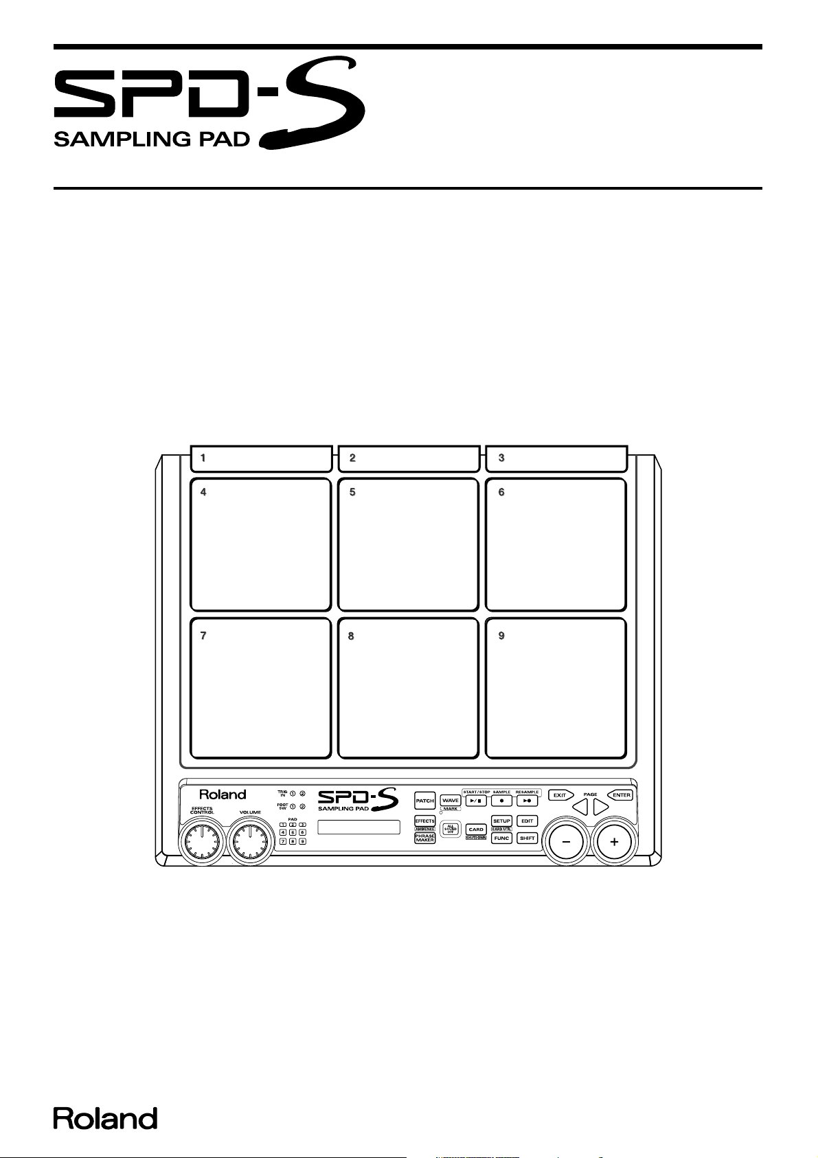
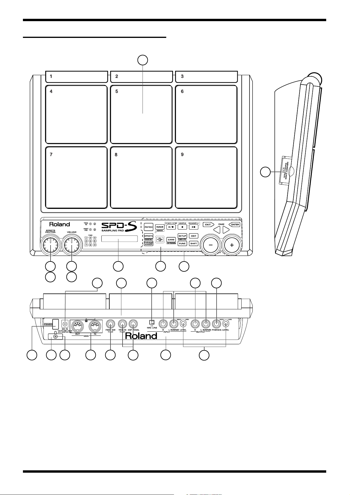
LOCATION OF CONTROLS
fig.panel
1
20
2
3
2
4
8
5
9
10
6
7
11
12
4
13
14
15
16
17
12
18
19
Page 5

LOCATION OF CONTROLS PARTS LIST
[Parts]
PART CODE PART NAME DESCRIPTION Q’TY
NO.
1 03341889 PLAYING PLATE ASSY for SC 1
2 03129489 R-KNOB for SC 2
3 03230601 9M/M ROTARY POT. EVUJFRFK1B14 1
4 F3229136 12M/M ROTARY POT. RV112B-40E1-125A-A10K for SC 1
5 03129756 PANEL SHEET ASSY for SC 1
6 03129545 TOP PANEL for SC 1
7 03129512 RUBBER SWITCH for SC 1
8 02341634 DC JACK HTJ-020-05A 1
9 03341890 BOTTOM CASE ASSY for SC 1
10 03235345 SLIDE SWITCH SSSF141300 1
11 02341712 6.5MM JACK (MONORAL) HTJ-064-10I 4
12 02897334 6.5MM JACK (STEREO) HTJ-064-10D for SC 3
13 12499175 KEY TOP for POWER SW JSPUE0011A 1
01676512 POWER SWITCH SDKLA1-B 1
14 22365714 CORD HOOK 1
15 40011312 SCREW M3x8 BINDING TAPTITE P BZC 1
16 02568867 MIDI CONNECTOR HDC-052A-12 1
17 02341645 6.5MM JACK (STEREO) HTJ-064-04A 1
18 03129556 REAR PANEL for SC 1
19 02565056 9M/M ROTARY POT. RK09K12A0D0K 2
20 03341901 CF COVER ASSY for SC 1
03121678 COMPACTFLASH CONNECTOR ICM-MA2H-SS52-R21A 1
03121689 COMPACTFLASH EJECTOR ICM-MAE-R21 1
SPD-S
5
Page 6
Apr.2003
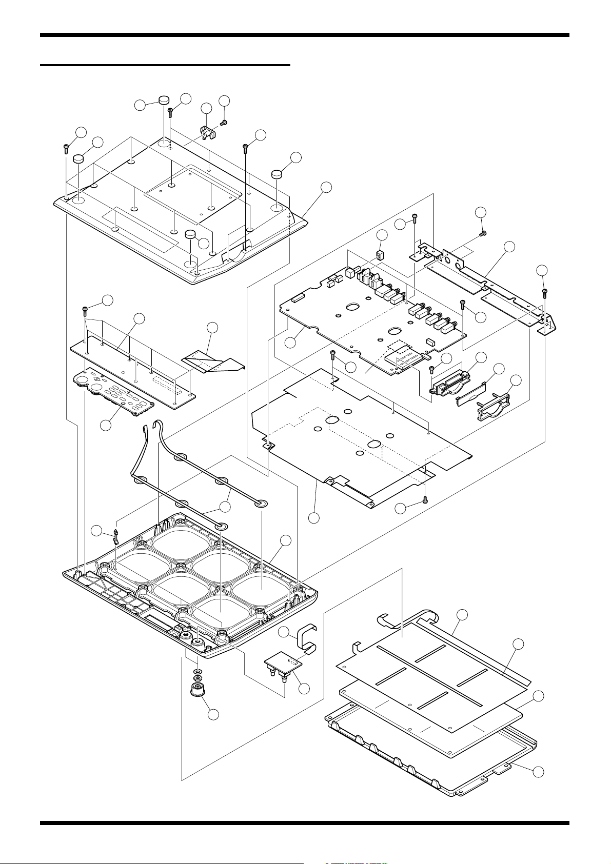
EXPLODED VIEW
fig.bunkai-e
2
b
2
c
11
a
e
1
f
2
3
c
c
2
12
6
d
5
4
c
d
c
*
7
8
9
14
13
19
15
18
16
17
10
d
* Apply SHIELD SHEET using a
double-side tape on the reverse side
20
21
22
6
23
Page 7

EXPLODED VIEW PARTS LIST
[Parts]
PART CODE PART NAME DESCRIPTION Q’TY
NO.
1 22365714 CORD HOOK 1
2 01344967 FOOT 4
3 03341890 BOTTOM CASE ASSY (INC. BOTTOM CASE) 1
4 ******** REAR HOLDER 1
5 12499175 KEY TOP for POWER SW JSPUE0011A 1
6 03129745 MAIN BOARD ASSY 1
7 03341901 CF COVER ASSY (INC. CF ESCUTCHEON) 1
8 03341901 CF COVER ASSY (INC. CF COVER) 1
9 03341901 CF COVER ASSY (INC. CF HOLDER) 1
10 ******** SHIELD SHEET 1
11 03129756 PANEL SHEET ASSY (INC. PANEL BOARD) 1
12 ******** WIRING 1 40 PIN 1
13 03129512 RUBBER SWITCH 1
14 03341889 PLAYING PLATE ASSY (INC. PCB SPACER CBS-19K) 3
15 03341889 PLAYING PLATE ASSY (INC. SENSOR ASSY) 2
16 03341889 PLAYING PLATE ASSY (INC. TOP CASE) 1
17 03129756 PANEL SHEET ASSY (INC. VOLUME BOARD) 1
18 ******** WIRING 2 12 PIN 1
19 03129489 R-KNOB for SC 2
20 03341889 PLAYING PLATE ASSY (INC. EDGE SHEET SENSOR for PAD 1-3) 1
21 03341889 PLAYING PLATE ASSY (INC. HEAD SHEET SENSOR for PAD 4-9) 1
22 03341889 PLAYING PLATE ASSY (INC. CUSHION) 1
23 03341889 PLAYING PLATE ASSY (INC. PLAYING PLATE) 1
SPD-S
[Screws]
NO. PART CODE PART NAME DESCRIPTION Q’TY
a 40562967 SCREW 4x16 BINDING TAPTITE P NI 4
b 40012501 SCREW 4x12 BINDING TAPTITE P BZC 11
c 40011278 SCREW 3x8 BINDING TAPTITE P ZC 16
d 40011056 SCREW 3x6 BINDING TAPTITE B ZC 9
e 40011312 SCREW 3x8 BINDING TAPTITE P BZC 1
f 02126156 SECURITY SCREW HEX CAP SCREW M3x10 TAPTITE P NI 2
7
Page 8

Apr.2003
PARTS LIST
fig.part1e
SAFETY PRECAUTIONS:
The parts marked have
safety-related characteristics. Use
only listed parts for replacement.
NOTE: The parts marked # are new. (initial parts)
CASING
03341889 PLAYING PLATE ASSY for SC 1
#
NOTE : ‘PLAYING PLATE ASSY’ INCLUDES ‘TOP PANEL’
# ******** EDGE SHEET SENSOR for PAD 1-3 1
# ******** HEAD SHEET SENSOR for PAD 4-9 1
# ******** CUSHON 1
# ******** PCB SPACER CBS-19K 1
# ******** PLAYING PLATE 1
# ******** SENSOR ASSY 2
# ******** TOP CASE 1
# 03129545 TOP PANEL 1
# 03341890 BOTTOM CASE ASSY for SC 1
NOTE : ‘BOTTOM CASE ASSY’ INCLUDES THE FOLLOWING PARTS
******** BOTTOM CASE 1
22365714 CORD HOOK 1
01344967 FOOT ^4
# 03129556 REAR PANEL 1
# 03341901 CF COVER ASSY 1
NOTE : ‘CF COVER ASSY’ INCLUDES THE FOLLOWING PARTS
# ******** CF COVER 1
# ******** CF ESCUTCHEON 1
# ******** CF HOLDER 1
CONSIDERATION ON PARTS ORDRING
When ordering any parts listed in the parts list, please specify the following items in the order sheet.
Failure to completely fill the above items with correct number and description will result in delayed or even
undelivered replacement.
QTY PART NUMBER DESCRIPTION MODEL NUMBER
Ex. 10 22575241 Sharp Key C-20/50
15 2247017300 Knob (orange) DAC-15D
Q’TY
KNOB, BUTTON
#
03129489 R-KNOB for SC 2
12499175 JSPUE0011A KEY TOP for POWER SW 1
JACK, EXT TERMINAL
#
03129512 RUBBER SWITCH for SC 1
01676512 PUSH SWITCH SDKLA1-B POWER SWITCH SW3 1
# 03235345 SLIDE SWITCH SSSF141300 SLIDE SWITCH SW2 1
SWITCH
PWB ASSY
POTENTIOMETER
CONNECTOR
02341645 HTJ-064-04A 6.5MM JACK (STEREO) JK9 1
02897334 HTJ-064-10D for SC 6.5MM JACK (STEREO) JK4,JK7,JK8 3
02341712 HTJ-064-10I 6.5MM JACK (MONORAL) JK2,JK3,JK5,JK6 4
02341634 HTJ-020-05A DC JACK JK10 1
02568867 HDC-052A-12 MIDI CONNECTOR JK1 1
#
03129745 MAIN BOARD ASSY for SC 1
# 03129756 PANEL SHEET ASSY for SC 1
02565056
# 03230601 EVUJFRFK1B14 9M/M ROTARY POT. VR4 1
# F3229136 RV112B-40E1-125A-A10K for SC 12M/M ROTARY POT. VR3 1
#
03121678
# 03121689 COMPACTFLASH EJECTOR ICM-MAE-R21 CN9 1
RK09K12A0D0K 9M/M ROTARY POT. VR1,VR2 2
COMPACTFLASH CONNECTOR
ICM-MA2H-SS52-R21A CN9 1
8
Page 9

SPD-S
WIRIING, CABLE
SCREW
PACKING
MISCELLANEOUS
ACCESSORIES (Standard)
******** WIRING 1 40 PIN 1
#
# ******** WIRING 2 12 PIN 1
40011056
40011278 SCREW M3x8 BINDING TAPTITE P ZC 16
40011312 SCREW M3x8 BINDING TAPTITE P BZC 1
40012501 SCREW M4x12 BINDING TAPTITE P BZC 11
# 40562967 SCREW M4x16 BINDING TAPTITE P NI 4
# 03341878 PACKING SET for SC 1
22365714
01344967 FOOT 4
# ******** SHIELD SHEET 1
03129701 OWNER’S MANUAL JAPANESE 1
#
# 03129712 OWNER’S MANUAL ENGLISH 1
# 03343323 LEAFLET JAPANESE/ENGLISH 1
00905756 AC ADAPTOR ACI-100C 1
00905767 AC ADAPTOR ACI-120C 1
01018312 AC ADAPTOR ACI-230C 1
01458278 AC ADAPTOR ACB-230E 1
12449549 AC ADAPTOR ACB-240(A) 1
# 03129723 CD-ROM SAMPLING CD for SC 1
# 40563778
02126156 SECURITY SCREW HEX CAP SCREW M3x10 TAPTITE P NI 2
# ******** HEXAGON WRENCH
# ******** SLIT TAPE 1
40232334 WARRANTY CARD (JAPAN ONLY) 1
SCREW M3x6 BINDING TAPTITE B ZC 9
CORD HOOK 1
STAND HOLDER MOUNTING SCREW
HEX CAP SCREW M5x12 BZC
4MM
4
1
9
Page 10
Apr.2003
1.
2.
3.
1.
2.
3.
4.
5.
IDENTIFYING THE VERSION NUMBER
Hold down the [ALL SOUND OFF] and [CARD] buttons and turn on the
power to the unit.
Press the [<]/[>] buttons to sequence through the display of the
following items.
• CPU Version, Build Number
fig.ver-1
CPU1.00 BLD0018
• CPU Release Date
fig.ver-2
CPU DATE 12/16/02
• CPU Release Time
fig.ver-3
CPU TIME 13:25:25
• EXT ROM Version, Build Number
fig.ver-4
PRG1.01 BLD0044
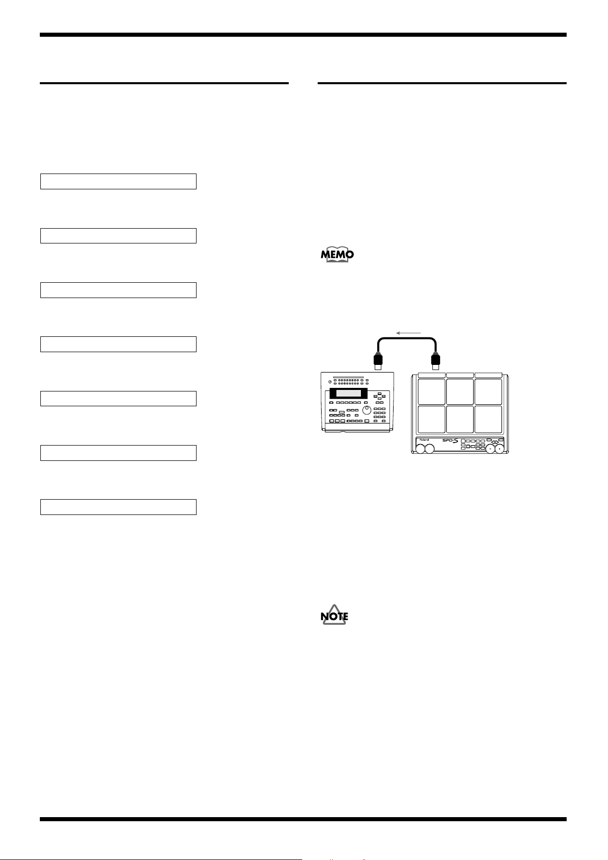
SAVING USER DATA & RELOADING SAVED DATA
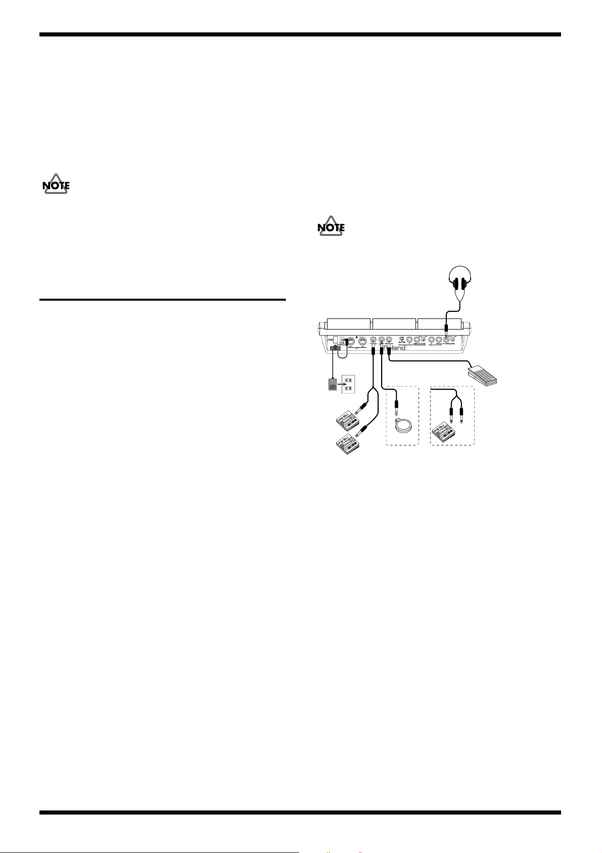
Required equipment
• MIDI sequencer
• MIDI cable
BULK DUMP
Settings for SPD-S setups and patches can be saved to an external MIDI device,
such as a sequencer.
Operate the external sequencer for recording ordinary performance data and
then take the following steps for the SPD-S.
See the operation manual of the external MIDI device for details on it.
Connect an external MIDI sequencer (as a saving destination) to the MIDI
OUT connector on the SPD-S using a MIDI cable.
fig.dump-e
• EXT ROM Release Date
fig.ver-5
PRG DATE 04/10/03
• EXT ROM Release Time
fig.ver-6
PRG TIME 08:39:14
• Factory Data Version, Build Number
fig.ver-7
PRE 1.17 BLD012
Turn off the power to quit.
MIDI IN MIDI OUT
External Seqencer
SPD-S
Set the SPD-S to the patch mode or to the wave mode.
Press [SETUP] button to access Setup Edit.
Press the PAGE buttons to select “BULK DUMP,” then press [ENTER]
button.
[+]
6.
7.
Press
Start recording on the external sequencer.
Press [>] button to display “bulk dump, sure?”
Press [ENTER] button to execute bulk dumping.
During transmission, “now sending” is displayed.
After the transmission is finished, a “complete!” indication appears and the
SPD-S returns to the “Dump” screen in Step 2.
To cancel the transmission midstream, press [EXIT] button.
8.
button to select “ALL”.
10
Stop the external sequencer to stop recording.
Page 11
SPD-S
Retrieving Saved Data Back to the SPD-S
Retrieves the settings saved to sequencers and other external MIDI devices to
the SPD-S.
Connect the MIDI IN connector on the SPD-S to the MIDI OUT connector
of an external sequencer using a MIDI cable.
Press [PATCH] button to enter patch mode.
Bulk data cannot be retrieved in any mode other than patch mode.
Transfer the settings data from the external sequencer to the SPD-S.
The transferred settings are restored.
TEST MODE
Required items
To quit Test mode:
Turn off the power to the unit.
* In each tested item, the screen initially shows the test type for a set length of
time, the display switches to the actual test screen.
* The “BelTreeD” sound is played when “OK” is returned and the procedure
advances to the subsequent test. When a test results “NG,” the “FlexMtl” sound
is played.
Test Mode Procedure
Executing Test mode deletes the User data; be sure to back up the data stored
in the unit beforehand.
fig.audio
• Expression Pedal (EV-5 etc.)
• Foot switch x3 (FS-5U etc.)
• PAD (With a RIM switch function) x2 (PD-7, PD-9, CY-12 etc.)
•Y cable (PCS-31) x2
• Stereo jack plug Cable x1
• Mono jack plug Cable x2
• MIDI cable
• CompactFlash (Formatting using the SPD-S)
• Monitor Speaker
• Headphone
Basic Test Mode Operations
Proceeding with series of test:
Some of tests automatically advance to the next when the result is “OK. ”
Press [>] button (the LED flashes as a prompt).
To advance to the next test forcefully even when the result is “NG” or
while running a test:
Hold down [SHIFT] button and press the [>] button.
To return to the previous test:
Roland
Stereo jack
plug cable
Pad with
a rim switch
Using a Y cable, connect two foot switches to the FOOT SW jack.
Make sure that the polarity is set properly here (set the foot switches to
open when the pedal is pressed; this should be the reverse of the TRIG IN
2.
3.
4.
5.
6.
switch).
1.
2.
3.
4.
Use a stereo cable to connect a pad with a rim switch to the TRIG IN jack.
Alternatively, use a Y cable to connect one foot switch to the TRIG IN
jack (plug in the Y cable’s red connector).
Make sure that the polarity is set properly here (set the foot switches to
short (close) when the pedal is pressed).
Connect an expression pedal to the EXP PEDAL jack.
Insert a CompactFlash card in the unit for tests.
Use a CompactFlash card formatted on the SPD-S.
If updating of the factory data is required in “0. Factory Data Update,”
use a CompactFlash card containing the factory data.
Y cable
or
red
white
1.
2.
3.
1.
Press the [<] button.
To return to the previous test forcefully:
Hold down [SHIFT] button and press the [<] button.
To repeat the current test:
Press [EXIT] button.
11
Page 12

Apr.2003
Entering Test Mode
Insert the CompactFlash card in the card slot.
Hold down both [PHRASEMAKER] and [CARD] buttons and turn on the
power.
Continue to hold down the buttons until [PATCH] and [EFFECTS]
buttons light.
Release [PHRASEMAKER] and [CARD] buttons.
Press [EXIT] button.
Press [ENTER] button.
Test Items
0. Factory Data Load
When the CompactFlash contains factory data, the instrument compares its
version with the version contained internally, and if the CompactFlash
contains a newer version, the unit automatically switches to Update mode.
If the data stored in the instrument is the later version, this mode is skipped.
fig.test0-1
New Factory Data
Press the [ENTER] button to begin loading.
fig.test0-2
[ENTER] to Update
Loading.
fig.test0-3
Now Loading...
When loading fails (in this case, press [EXIT] button to return to the previous
screen).
fig.test0-4
Load Failed!
When loading completes normally, the process automatically advances to
the subsequent test.
fig.test0-5
Load Completed!
2. Device Test
fig.test2-1
2.Device Test
When the test results “OK”, the “-” symbol changes to “o”; if the test
results “NG” (fail), the symbol changes to a charactor to represent the
error type.
fig.test2-2
DEV [------]
fig.test2-3
DEV [ooSoWC] NG!
Checked Items
I: CPU Internal: Checksum Comparison
P: Program ROM: Checksum Comparison
S: SDRAM: Write/Read
M: MR3 Chip: Write/Read
N: NAND Flash: Write/Read/Format
C: CompactFlash: Format (Write/Read Check)
Press the [>] button to show which tests failed.
If multiple tests fail, use the [<] and [>] buttons to navigate (the [<] and
[>] buttons flash as a prompt).
fig.test2-4
CPU Internal NG!
fig.test2-5
Program ROM NG!
If all tests result “OK,” the process automatically advances to the
subsequent test.
fig.test2-6
DEV [oooooo] OK!
1.
2.
1.
2.
3.
4.
5.
6.
2.
1.
2.
1.
3.
1.
2.
3. MIDI Test
fig.test3-1
3.MIDI Test
1. Version Test
fig.test1-1
1.Version Test
Confirm the version number.
fig.test1-2
CPU1.00 PRG1.01
Press the [>] button to advance to the subsequent test.
12
Use a MIDI cable to connect SPD-S‘s MIDI IN and MIDI OUT.
Before Connecting
fig.test3-2
MIDI OUT-x-IN
Connected
fig.test3-3
MIDI OUT---IN OK
If the test results “OK,” the process automatically advances to the
subsequent test.
Page 13

SPD-S
4. Switch/LED Test
fig.test4-1
4.SW/LED Test
fig.test4-2
(22)
The number of switches that have not been checked is indicated in
parentheses.
Using a Y cable, connect two foot switches to the FOOT SW jack.
Use a stereo cable to connect a PD-7 to the TRIG IN jack.
Alternatively, use a Y cable to connect one foot switch to the TRIG IN
jack (plug in the Y cable’s red connector).
Press the panel switches individually to comfirm that the name of the
switch being pressed appears in the display and that the corresponding
sound is played.
If the switch includes an LED, also confirm that the LED turns off when
the switch is pressed.
* For pad switches, press (grasp) the rim section.
* The test doesn't result “OK” when two or more panel switches are pressed
simultaneously.
The test also doesn't result “OK” when the foot switches (or a foot switch and
pad switch) are pressed simultaneously.
fig.test4-3
(14) ALLSOUNDOFF
5. Effects Control Knob Test
fig.test5-1
5.CtrlKnob Test
Turn the [EFFECTS CONTROL] knob completely to the left
(counterclockwise), and confirm that the value is “0” when the knob is
fully turned.
fig.test5-2
KNOB (108)
The following screen appears when the knob is turned fully to the left.
At this time, confirm that the “CowbMmbo” sound is played.
fig.test5-3
KNOB (0)
Turn the [EFFECTS CONTROL] knob completely to the right.
At this time, confirm that the “BelTreeD” sound is played.
If the test results in “OK,” the process automatically advances to the
subsequent test.
fig.test5-4
KNOB (127) OK!
6. Expression Pedal Test
fig.test6-1
6.Exp.Pedal Test
The PAD LEDs turn off with each press of the [+] button.
Confirm that all of the PAD LEDs go off.
fig.test4-4
(0) + (PAD1 LED)
Switches
fig.test4-5
[PATCH] [WAVE] [PLAY/STOP] [SAMPLE]
[RESAMPLE] [EXIT] [ENTER]
[EFFECTS] [ALLSOUNDOFF] [CARD] [SETUP]
[EDIT] [LEFT/<] [RIGHT/>]
[PHRASEMAKER] [FUNC] [SHIFT] [-] [+]
[FOOTSW1] [FOOTSW2] [TRIGINSW]
If all of the switches pass their tests, the process automatically advances
to the subsequent test.
fig.test4-6
(0) OK!
Connect an expression pedal to the EXP PEDAL jack.
Confirm that the value is “0” when the pedal heel is pressed down fully.
fig.test6-2
PEDAL (108)
The following screen appears in the display when the pedal heel is
pressed down fully.
At this time, confirm that the “CowbMmbo” sound is played.
fig.test6-2
1.
2.
3.
PEDAL (0)
Press the pedal toe down completely.
At this time, confirm that the “BelTreeD” sound is played.
4. If the test results in “OK,” the process automatically advances to the
subsequent test.
fig.test6-3
PEDAL (127) OK!
4.
5.
1.
2.
3.
1.
2.
3.
13
Page 14

Apr.2003
7. LCD Test
fig.test7-1
7.LCD Test
1. Hold down the [INC/+] button and confirm that the LCD contrast
changes gradually.
Holding down the [INC/+] button and pressing the [DEC/-] button
causes the contrast to change more rapidly.
When the contrast is at the maximum level, the screen shown below
appears.
At this time, confirm that the “Agogo Hi” sound is played.
fig.test7-2
2. Hold down the [DEC/-] button and confirm that the LCD contrast
changes gradually.
Holding down the [DEC/-] button and pressing the [INC/+] button
causes the contrast to change more rapidly.
When the contrast is at the minimum level, the screen shown below
appears.
At this time, confirm that the “Agogo Lo” sound is played.
fig.test7-3
______________________
8. Trigger Test
fig.test8-1
8.Trigger Test
1. Using a Y cable, connect two pads to the TRIG IN jack.
To disable the trigger while connecting or disconnecting the cable, hold down
the [FUNC] button; the trigger is ignored while this button is pressed.
fig.test8-2
Hit "Softly"
fig.test8-3
123456789AB Soft
2. Sheet Sensor Check
The test automatically checks whether or not the sheet sensor is turned
on while the pad is not being touched.
If no pad has a sheet sensor on, nothing appears in the display, and the
procedure advances to the subsequent test.
3. Press the [ENTER] button and confirm that the entire LCD is lit (the
[ENTER] button flashes as a prompt).
At this time, confirm that the “Shaker” sound is played.
fig.test7-2
4. Press the [ENTER] button and confirm that the entire LCD goes dark (the
[ENTER] button flashes as a prompt).
At this time, confirm that the “Maracas” sound is played.
fig.test7-4
* Pressing the [ENTER] button cycles through the contrast check, all LCD on,
and all LCD off tests.
5. If all tests result in “OK,” press the [>] button to advance to the
subsequent test.
The procedure does not advance unless all of the above tests are
completed.
Do not touch the pads while the check is in progress.
If there is a pad with its sheet sensor on, the pad’s number is displayed,
the pad LED flashes, and the test result is “NG.”
fig.test8-4
oo3oo67oo Sheet
3. Check response to weak hits by striking a lightly and individually.
Confirm that the corresponding number disappears and that the
corresponding sound is played.
The LED for each corresponding pad flashes and then goes off.
fig.test8-5
___456789AB Soft
The test does not result “OK” when two or more pads are struck
simultaneously.
A minimum interval of 0.1 seconds is required between each stroke of the
pads.
14
When a pad is struck hard, the corresponding number in LCD doesn’t go off
and no sound is played although the pad LED lights, and the test doesn’t
result “OK.”
4. If all pads are “OK,” the process automatically advances to the
subsequent test.
fig.test8-6
Hit "Hard"!
fig.test8-7
123456789AB Hard
Page 15

SPD-S
5. Check response to strong hits by striking a pad hard and individually.
Confirm that the corresponding number disappears and that the
corresponding sound is played.
The LED for each corresponding pad flashes and then goes off.
fig.test8-8
___456789AB Hard
When a pad is struck lightly, the corresponding number in LCD doesn’t go off
and no sound is played although the pad LED lights, and the test doesn’t
result “OK.”
The weak and strong checks can be switched by pressing the [ENTER] button.
Correspondence Between the Pads and
Sounds
fig.test8-9
[1: Claves 2 ] [2: CowbMmbo ] [3: Agogo Hi ]
[4: Bongo Hi ] [5: Conga Hi ] [6: Xstick 3 ]
[7: 808Kik 1 ] [8: eSnr ] [9: AcuHH cl ]
[A(Trig1): 909Claps ] [B(Trig2): SpokTom1 ]
6. If all pads are “OK,” the process automatically advances to the
subsequent test.
fig.test8-10
[___________] OK!
Advanced Test Mode
To enter Advanced Test mode, press the [ALLSOUNDOFF] button during the
Trigger Test.
This mode, you may check the causes of failure in the above test.
a. Sheet Sensor Check
If a pad’s sheet sensor turns on when the pad is pressed with the hand,
the corresponding number disappear, and the pad’s LED goes off.
Release the pads to return them to their original state.
fig.test8-11
123456789 Sheet
Hand-press [Pad3].
fig.test8-12
12_456789 Sheet
Release [Pad3].
fig.test8-11
123456789 Sheet
b. Velocity Check
Strike each pad with a stick; when a pad is struck, the pad number and
velocity value (1--127) is displayed, and the corresponding LED flashes
and then goes off.
fig.test8-13
( ) Velo( )
Strike [Pad5].
fig.test8-14
(Pad5) Velo(115)
When a pad has faulty sheet sensors that does not turn on, there is no response
from the pad when it is struck.
Press the [ALLSOUNDOFF] button to return to the Sheet Sensor Check.
Press the [EXIT] button to return to the beginning of the Trigger Test.
9. Audio Input Test
fig.test9-1
9.Audio In Test
1. Set the [VOLUME] knob to minimum, and turn the [INPUT LEVEL] knob
on the rear panel to the maximum setting.
2. Use two mono cables to connect the INPUT L/MONO and R to the
OUTPUT L/MONO and R.
fig.test9-2
Set Volumes MIN
3. Press the [ENTER] button.
fig.test9-3
[MIC] <- [LINE]
fig.test9-4
(Level Meter Display)
Above level meter is displayed, and a 100-Hz signal is output at -50 dBu.
The [START/STOP] button flashes.
4. Set the [LINE/MIC] switch to “MIC” and turn up [VOLUME] knob.
If the signal level is correct when [VOLUME] knob is turned right fully,
the process automatically advances to the subsequent test.
The level meter is displayed in the LCD.
fig.test9-4
(Level Meter Display)
Press the [ALLSOUNDOFF] button to advance to the Velocity Check.
5. The LCD shows following display, then it returns to the level meter.
fig.test9-5
[MIC] -> [LINE]
A 100-Hz signal is output at -10 dBu.
[START/STOP] button lights, and [SAMPLE] button flashes.
15
Page 16

Apr.2003
6. Set [LINE/MIC] to “LINE.”
If the signal level is correct, the signal automatically switches to 10 kHz,
and the same test runs.
The [START/STOP] and [SAMPLE] buttons light, and the [RESAMPLE]
button flashes.
If the tests result is “OK,” the process automatically advances to the
subsequent test.
In this test, signal status is normal when six squares are displayed for both the
left and right channels in the LCD.
At this time, the [WAVE] button lights.
10. Sound Test
fig.test10-1
10.Sound Test
1. Confirm that no sound is being played ([ENTER] LED flashes as a
prompt).
fig.test10-2
SOUND
2. Press [ENTER] button, and confirm that a sine wave is output from both
the left and right channels of OUTPUT and PHONES (the [EDIT] button
lights).
fig.test10-3
<<L SOUND R>>
11. Completing Test Mode
1. If all of the tests in Test mode result in “OK”, shutdown for the card is
executed.
fig.test11-1
shutdown..
fig.test11-2
shutdown.. OK!
When the following is displayed, turn off the power to the unit.
fig.test11-3
Test Completed!
2. If any of the tests fails, the following is displayed.
fig.test11-4
Not All Passed
INITIALIZATION PROCEDURE
Resets the SPD-S’s settings to initial values, or delete all the data stored in the
SPD-S.
If you execute INIT/DELETE to delete patches and waves from the internal
memory, the SPD-S will produce no sound.
3. Press the [EDIT] button, and confirm that the output is muted (the mute
circuits activate).
At this time, the sound is output at a very low level; this does not indicate any
malfunction (the [ENTER] LED lights as a prompt).
fig.test10-4
<<L MUTE R>>
4. Press [ENTER] button, and confirm that a sine wave is output only from
the left channel of OUTPUT and PHONES (the [ENTER] LED lights as a
prompt).
fig.test10-5
<<L SOUND
5. Press [ENTER] button, and confirm that a sine wave is output only from
the right channel of OUTPUT and PHONES (the [ENTER] LED lights as a
prompt).
fig.test10-6
SOUND R>>
6. Press [ENTER] button, and confirm that no sound is being output (the
[ENTER] LED lights as a prompt).
fig.test10-7
SOUND
1. Set the SPD-S to the patch mode or to the wave mode.
2. Press [SETUP] button to access Setup Edit.
3. Press the PAGE buttons to select “INIT/DELETE,” then press [ENTER]
button.
[+]
5.
6.
4. Press
Press [>] button to display “delete all, sure?”
Press [ENTER] button to start initialization or deletion.
During execution, “now processing?” is indicated.
After the execution, a “complete!” indication appears, and the SPD-S
returns to the patch mode.
Do not power the SPD-S off during execution.
7.
button to select “ALL.”
* Press [ENTER] button to cycle through Steps 3--6.
7. If the tests result “OK,” press [>].
16
Page 17

SPD-S
FORMATTING A COMPACTFLASH CARD
To insert a CompactFlash card, carefully open the card slot cover (lefthand side of the SPD-S).
fig.cf-1
MEMORY CARD slot
CompactFlash™
Select patch mode or wave mode.
Press [SHIFT] and [SETUP] buttons (CARD UTIL).
RESTORING THE FACTORY SETTINGS
The accompanying CD contains audio signals for sampling on the SPD-S and
digital data for restoring the SPD-S to its factory settings.
Restoring Patches and Waves to the Factory Settings
Once you execute this operation, you will lose all the patches and waves stored
in the internal memory.
Back up such data beforehand if needed.
Required items
•A computer with a CD-ROM drive
•A card reader that supports CompactFlash cards
• The accompanying CD-ROM (P/No.03129723)
• CompactFlash (Formatted using the SPD-S)
Procedure
Connect the card reader to the computer to ensure that it can be used.
If no CompactFlash card has been inserted, “no card!” is indicated and the
SPD-S returns to the original mode.
Press the PAGE buttons to select “CARD FORMAT,” then press [ENTER]
button.
When the CompactFlash card is unformatted, only “CARD FORMAT” is
displayed.
A “[>] to format.” indication appears. Press [>] button.
A “format, sure?” indication is displayed. Press [ENTER] button to start
formatting.
While formatting is in progress, “now processing..” is displayed. Then,
the SPD-S returns to the original mode.
For connecting the card reader to the computer and using them, see their
respective operation manuals.
Load the accompanying CD into the CD-ROM drive.
Insert the CompactFlash card into the card reader.
Copy the “FCTRY” folder on the accompanying CD to the “ROLAND”
folder on the CompactFlash card.
If the “ROLAND” folder on the CompactFlash card already has a
“FCTRY” folder, delete the “FCTRY” folder before copying.
Eject the CompactFlash card to which the copying was done in Step 4
from the card reader.
Then, make sure that the SPD-S is powered off and insert it into the card
slot of the SPD-S.
While holding down [PATCH], [WAVE], and [CARD] button ON the
SPD-S.
After powering it on, hold down the three buttons until “[ENTER] to Load”
appears.
“[ENTER] to Load” appears. Release the three buttons. Next, press
[ENTER].
Data transfer from the CompactFlash card to the SPD-S begins.
It takes a few minutes until it is complete.
1.
2.
3.
1.
2.
3.
4.
5.
7.
4.
5.
6.
8.
6.
During the data transfer, do not eject the CompactFlash card from the card slot
and do not switch off power to the SPD-S. Doing so could not only destroy the
data, but also cause problems for the SPD-S.
“Load Completed!” appears, and the data transfer is complete.
Now, eject the CompactFlash card, power the SPD-S off, then power it on
again.
17
Page 18

Apr.2003
PROCEDURE FOR UPDATING THE SYSTEM SOFTWARE
The system can be updated using CompactFlash or MIDI.
Instructions for Updating Using CompactFlash
5.
When the update is completed normally, the [START/STOP], [SAMPLE],
and [RESAMPLE] LEDs light up.
fig.up-3
Update Complate
If an error occurs during the procedure, all of the LEDs light up, and an
error message is displayed.
fig.up-4
Update ERROR 15
Required items
•A computer with a CD-ROM drive
•A card reader that supports CompactFlash cards
• UPDATE CD-ROM for CF Card (P/No.17041324)
• CompactFlash (Formatted using the SPD-S)
1. Preparation
Prepares a CompactFlash card containing the updated system file.
Insert the CompactFlash in a card reader connected to a computer.
For instructions on connecting the computer and card reader, refer to the
service notes for formatting a CompactFlash.
Place the updated program in the CompactFlash’s root (the top level).
This completes preparation of the updater CompactFlash.
2. Update Procedure
Hold down the [EFFECTS] and [ENTER] buttons and turn on the power
to the unit.
The [PATCH] and [PHRASEMAKER] buttons flash.
fig.up-1
Card Updater
* To cancel the update at this point, turn off the power to the SPD-S.
6. Turn off the power to end the procedure.
Updating Using MIDI
Required items
•A MIDI sequencer that can play back SMF data
• UPDATE CD-ROM for SMF (#17041324)
• MIDI Cable
1. Preparation
The following sixteen files are required for the updater SMF; confirmed that
they are present.
p00001.mid, p00002.mid, p00003.mid, p00004.mid
p00005.mid, p00006.mid, p00007.mid, p00008.mid
p00009.mid, p00010.mid, p00011.mid, p00012.mid
p00013.mid, p00014.mid, p00015.mid, p00016.mid
2. Update Procedure
1. Use a MIDI cable to connect the MIDI OUT connector of a sequencer
capable of playing back SMFs and the MIDI IN connector on the SPD-S.
2. Hold down the [WAVE] and [ENTER] buttons and turn on the power to
the unit.
3. The [SETUP] and [EDIT] buttons flash.
fig.up-5
MIDI Updater
1.
2.
1.
2.
3.
4.
Press the [PATCH] and [PHRASEMAKER] buttons simultaneously.
The update begins.
The process is divided into sixteen steps, and in each step, the
[START/STOP] -> [SAMPLE] -> [RESAMPLE]
LEDs light in sequence.
fig.up-2
Update: **/16
* The “**” indicates the step number currently being processed (01--16).
18
* To cancel the update at this point, turn off the power to the SPD-S
4. Press the [SETUP] and [EDIT] buttons simultaneously.
fig.up-6
Please Send
5. Play back p00001.mid through p00016.mid in sequence.
6. The update begins, and with each file, the
[START/STOP] -> [SAMPLE] -> [RESAMPLE]
LEDs light in sequence.
fig.up-2
Update: **/16
* The “**” indicates the file currently being executed (01--16).
Page 19

7. When the update is completed normally, the [START/STOP], [SAMPLE],
and [RESAMPLE] LEDs light up.
fig.up-3
Update Complate
If an error occurs during the procedure, all of the LEDs light up, and an
error message is displayed.
fig.up-4
Update ERROR 15
8. Turn off the power to end the procedure.
SPD-S
19
Page 20

Apr.2003
SPD-S
BLOCK DIAGRAM
fig.block
clk=50MHz
CPU
V850E/MA1
LINE IN
L(MONO)
LRCK
MCK
16bit
V850E GA
SYI
8bit
Gate Array DSP
BCK
8bit
LINE IN
R
LINE -10dBu
MIC -50dBu
LINE/MIC
w.F SR
FOOT
SW
(1/2)
w.F SR
w.FSR
w.FSR
F SR Only
F SR Only
TRIG IN
(1/2)
w.F SR
F SR Only
w.F SR
EXP PEDAL
EFFECTS
CONTROL
BCK
MCK
LRCK0
XP-LRCK
PAD4
PAD5
PAD6
PAD7
PAD8
PAD9
PAD 1
PAD 2
PAD 3
SW Matrix
(RUBBER)
AD/DA
CODEC
24bit/512fs/GD=15.4
MAIN BOARD
INPUT
LEVEL
NJM78L05UA
DC IN
ACI or ACB
9V/1000mA
NJM2360AM
DC-DC
NJM2360AM
DC-DC
POWER SW
Others Parts
@40
Others Parts
@40
REGULATOR
RIPPLE
FILTER
RESET IC
PHONES
LEVEL
VOLUME
OUTPUT
R
OUTPUT
L
(MONO)
LINE +4dBu
PHONES +15dBu
PHONES
LRCK1
128Mbit
NAND FLASH
for Preset,User Wave
System Parameter
ComapctFlash
for Patch,Wave Storage
16bit
BUS BUFFERS
8Mbit
NOR FLASH
16Mbit
SDRAM
16bit16bit
for Cache/Work/Delay Line for Program
MIDI
PANEL SHEET
(PANEL BOARD)
LCD
RCM2122M-1A
/RCM2122M-A
16x1 Charactor
LED Matrix
PANEL SHEET
(VOLUME BOARD)
UPD70F3107AGJ-UEN (SPD-S 1.01)
P2
RIM3
RIM1
RIM2
P1
RIM5
RIM6
RIM9
RIM4
RIM8
RIM7
RIM10
MXPAD
RIM[1..10]
P1
P2
MXPAD
XRESET
ANI7
ANI4
ANI6
ANI5
ANI0
ANI2
ANI1
ANI[0..7]
ANI3
MIDI_IN
XRESET
MIDI_OUT
A
A
A
A
+
5D
+
D3
.
3
A
A
A
A
A
+
D3.3
+
D3.3
+
A9
+
A9
+
D3.3
+
D3.3
+
D3.3
+
D3.3
+
D3.3
+
D3.3
+
D3.3
+
D3.3
+
D3.3
+
D3.3
+
D3.3
+
D3.3
A
+
5D
+
D3.3
-
9A
+
A9
A
A
A
+
D3.3
+
D3.3
+
D3.3
+
5D
+
5D
+
5D
+
5D
+
5D
+
D3.3
21
22
23 11
12
13
21
22
23
fx=5MHz
1 4
1 2
1/50
1
2
4
1
2
4
11
12
13
+
-
2
3
1
M5218AFP
+
-
6
5
7
M5218AFP
+
-
2
3
1
M5218AFP
+
-
6
5
7
M5218AFP
+
-
2
3
1
21
22
23
11
12
13
1 2
BA10324AF
+
-
13
12
14
1 2
1 2
1
2
3
4
5
7
8
1 2
1 2
1 2
1 2
1 2
1
2
3
1
2
3
BA10324AF
+
-
9
10
8
1 2
1
2
3
1 2
RT1N141C
1
2
3
R?
10k
M5218AFP
+
-
6
5
7
0.1
2
1
3
12
0.1
S-80927CLMC-G6X-T2
CD
5
VCC
2
GND
3
OUT
1
NC
4
12
11
13
1
2
4
1
2
4
1
2
3
M5216FP
+
-
6
5
7
M5216FP
+
-
2
3
1
M5218AFP
+
-
6
5
7
M5218AFP
+
-
2
3
1
RIN
1
LIN
2
VSS
3
VA
4
VD
5
DEMO
6
DEM1
7
SDTO
8
SDTI
9
LRCK
10
MCLK
11
BCLK
12
PDN
13
VCOM
14
LOUT
15
ROUT
16
11.2896MHz(256fs)
1 2
BA10324AF
+
-
2
3
1
BA10324AF
+
-
6
5
7
M5218AFP
+
-
2
3
1
M5218AFP
+
-
6
5
7
M5218AFP
+
-
2
3
1
M5218AFP
+
-
6
5
7
BA10324AF
+
-
6
5
7
BA10324AF
+
-
9
10
8
BA10324AF
+
-
13
12
14
BA10324AF
+
-
2
3
1
PC410
64
1
3
5
120
100
220
220
2.2k
RT1P141C
1
3 2
HD74LS05FP
12
HD74LS05FP
12
HD74LS05FP
12
10k
2
4
5
INOUT
2
4
5
12
14
15
22
24
25
304050
60
1 2
CD4053BCSJ
1Y
1
0Y
2
1Z
3
ZCOM
4
0Z
5
INH
6
VEE
7
VSS
8
C
9
B
10
A
11
0X
12
1X
13
XCOM
14
YCOM
15
VDD
16
10 10
100k
+
D3
+
D3
M5218AFP
+
D3
.
3
+
D3
.
3
+
D3
.
3
XPDN
20 21
Page 21

Apr.2003
SPD-S
CIRCUIT BOARD (MAIN)
fig.main-comp-slk
View from components side
22 23
Page 22

Apr.2003
SPD-S
CIRCUIT BOARD (MAIN)
fig.main-foil-ptn
View from foil side
24 25
Page 23

Apr.2003
SPD-S
CIRCUIT DIAGRAM (MAIN 1/8)
fig.main1-c
CPU - V850E/MA1
Trigger Section
SDRAM
16Mb
FLASH
8Mb
SDRAM
64/128Mb
(TC59SM716AFT-80)
(A)
(A)
(B)
(B)
CPU FLASH WRITER
(LH28F160BJE)
(LH28F320BFE)
CF I/F Section
GA&DSP Section
Audio Section
Jack Section
CN Section
(A)
(B)
64Mbit 128Mbit
0
NIU
NIU
0
16Mbit
NIU
NIU
Under Development Only
*SW1 SSSS222-01-A
*CN1 IL-S-7P-S2T2-EF
*C322 100u
*R255 10k
*C17 0.1u
*R1,R24 Pattern cut
(Trial)
UPD70F3107AGJ-UEN (SPD-S 1.00) (1Lot-1.99Lot)
UPD703106AGJ-066-UEN (SPD-S) (2Lot-)
IC3
IC5
Mounting
NIU
NIU NIU
Mounting Mounting
DQ0
SD_CKE
EEP_SCK
EEP_SDA
D5
A15
A13
A14
A11
A12
D15
D12
D15
D2
D12
D4
D14
D6
D0
D5
D1
D11
D3
D9
A13
D7
D9
D6
A12
D13
A10
A14
D10
D11
D8
D0
A15
A11
D10
A10
D7
D8
D2
D13
D3
D4
D14
D1
D11
D8
A11
A12
D4
D15
D7
D13
D9
D6
A14
A10
D1
A15
D12
D2
D10
A13
D3
D5
D14
D0
DQ1
DQ2
DQ3
DQ4
DQ5
DQ6
DQ7
DQ8
DQ9
DQ10
DQ11
DQ12
DQ13
DQ14
DQ15
XSD_RAS
XSD_CS
A11
A10
SD_CLK
DQ0
DQ1
DQ2
DQ3
DQ4
DQ5
DQ6
DQ7
DQ8
DQ9
DQ10
DQ11
DQ12
DQ13
DQ14
DQ15
SD_CKE
XSD_RAS
XSD_CS
SD_CLK
A11
A10
BA1
BA2
MIDI_OUT(SO0)
MIDI_OUT(SO0)
SI0
XFZ_RST
SCK0
XSD_CAS
XSD_CAS
A18
A19
A18
A20
A19
A18
A17
A22
A17
A21
A23
A20
A23
A22
A20
A17
A22
A23
A22
A12
A21
A16
A21
A16 A16
A19
ANI7
SD0
ANI4
ANI6
ANI2
XDMARQ3
XDMARQ0
SS0
XDMARQ1
FZ_VPP
P1
SS1
ANI3
SD4
ANI5
SCK0
P2
SD3
SS2
ANI1
ANI0
SD2
SS3
SD1
XDMAAK1
XDMAAK0
RIM9
RIM8
RIM7
RIM6
RIM5
RIM4
RIM3
RIM2
RIM1
RIM10
FL_VPP
XRESET
XFL_CS
SD_CKE
XSD_CS
XFL_CS
SD_CKE
XSD_RASXSD_RAS
SD_CLKSD_CLK
XSD_CAS XSD_CAS
FL_VPP
EEP_SDA
EEP_SCK
EEP_SDA
EEP_SCK
A8 A8
A7
A2
A6
A5
A1
A0
XDMAAK0
A5
A6
XDMARQ3
A4
A5
A5
A9
A3
A4
A1
A6
XGA_CS
A7
XDMAAK1
A1
A2
A4A4
A1
A3
A8
A4
A8
A7
D[0..15]
A9
A3
A7
A[0..9]
XNF_CS
A2
XDMARQ0
A5
A1
A9
A3
A2
A9
A7
A9 A8
A0
A3 A2
A6
A6
XDSP_CS
XWAIT
XCF_CS
SD2
SD0
SS3
SS2
SD4
SS1
SD1
SS0
SD3
AMUTE
FL_R/XB
FL_R/XB
'CF_R/XB
'XCF_SC
CF_RESET
FZ_VPP
XCF_DETECT
XSD_CS
XFL_CS
XGA_CS
XNF_CS
XCF_CS
XDSP_CS
LDQM/XLWR
LDQM/XLWR
GA_CLK
XBCYST
UDQM
GA_CLK
XBCYST
XWAIT_EN
LDQM/XLWR
XWE
UDQM
XWE
XWAIT_EN
XWE
UDQM
XRD
UDQM
XRD
XWE
LDQM/XLWRLDQM/XLWR
XRD
XFL_WP
CF_XATA/IDE
XFL_WP
XCF_OEGATE
XFL_WP
CF_XATA/IDE
XCF_OEGATE
XFZ_RST
SI0
CF_XON/OFF CF_RESET
CF_RESETZ
XDMARQ1
XPDN
'LCDCONT
XRESET
MIDI_IN
D D
D
+
D3.3
D
+
D3.3
D
D
D
D
+
D3.3
+
D3.3
D
+
D3.3
+
D3.3
D
+
D3.3
D
+
D3.3
+
D3.3
D
+
D3.3
D
D
D
+
D3.3
D
+
D3.3
+
D3.3
D
+
D3.3
D
+
D3.3
+
D3.3
D
D
D
+
D3.3
+
D3.3
+
D3.3
D
D
D D
D
R23
10k
C28
0.1
C29
0.1
C23
0.1
C30
0.1
C26
0.1
C24
0.1
C27
0.1
C22
0.1
C25
0.1
C21
100p
C19
SLP@M
10/16
C31
SLP@M
10/16
RA4
10k
1234567
8 9
10111213141516
IC1
HN58X2408FPI
NIU
A0
1
A1
2
A2
3
VSS
4
SDA
5
SCL
6
WP
7
VCC
8
C12
1
RA10
22
1
2
3
4
5
6
7
8 9
10
11
12
13
14
15
16
RA3
10k
1234567
8 9
10111213141516
C13
SLP@M
10/16
RA7
22
1
2
3
4
5
6
7
8 9
10
11
12
13
14
15
16
C111C101C91C81C7
1
IC3
GLT5160L16-7TC
VDD
1
VSSQ
4
VDDQ
7
VSSQ
10
VDDQ
13
LDQM
14
WE
15
CAS
16
RAS
17
CS
18
BA
19
A10/AP
20
VDD
25
VSS
26
NC
33
CKE
34
CLK
35
UDQM
36
NC/RFU
37
VDDQ
38
VSSQ
41
VDDQ
44
VSSQ
47
VSS
50
DQ15
49
DQ14
48
DQ13
46
DQ12
45
DQ11
43
DQ10
42
DQ9
40
DQ8
39
DQ7
12
DQ6
11
DQ5
9
DQ4
8
DQ3
6
DQ2
5
DQ1
3
DQ0
2
A0
21
A1
22
A2
23
A3
24
A4
27
A5
28
A6
29
A7
30
A8
31
A9
32
IC5
(M2V64S40DTP-7)
NIU
VDD
1
DQ0
2
VDDQ
3
DQ1
4
DQ2
5
VSSQ
6
DQ3
7
DQ4
8
VDDQ
9
DQ5
10
DQ6
11
VSSQ
12
DQ7
13
VDD
14
DQML
15
WE
16
CAS
17
RAS
18
CS
19
BA0(A13)
20
BA1(A12)
21
A10
22
A0
23
A1
24
A2
25
A3
26
VDD
27
VSS
28
A4
29
A5
30
A6
31
A7
32
A8
33
A9
34
A11
35
NC
36
CKE
37
CLK
38
DQMU
39
NC
40
VSS
41
DQ8
42
VDDQ
43
DQ9
44
DQ10
45
VSSQ
46
DQ11
47
DQ12
48
VDDQ
49
DQ13
50
DQ14
51
VSSQ
52
DQ15
53
VSS
54
R15
NIU
R13
NIU
R11
NIU
R12
NIU
CN1
B7B-PH-K-S
NIU
1
1
2
2
3
3
4
4
5
5
6
6
7
7
RA9
10k
1
2
3
4
5
6
7
8 9
10
11
12
13
14
15
16
RA12
22
1
2
3
4
5
6
7
8 9
10
11
12
13
14
15
16
RA1
47
1
2
3
4
5
6
7
8 9
10
11
12
13
14
15
16
RA11
22
1
2
3
4
5
6
7
8 9
10
11
12
13
14
15
16
X1
SD3@
5MHz
1 2
RA2
10k
1
2
3
4
5
6
7
8 9
10
11
12
13
14
15
16
RA6
10k
1
2
3
4
5
6
7
8 9
10
11
12
13
14
15
16
R10
10k
IC4
LH28F800BJE-PBTL90@
A15
1
A14
2
A13
3
A12
4
A11
5
A10
6
A9
7
A8
8
NC
9
NC
10
WE
11
RP
12
VPP
13
WP
14
RY/BY
15
A18
16
A17
17
A7
18
A6
19
A5
20
A4
21
A3
22
A2
23
A1
24
A0
25
CE
26
GND
27
OE
28
DQ0
29
DQ8
30
DQ1
31
DQ9
32
DQ2
33
DQ10
34
DQ3
35
DQ11
36
VCC
37
DQ4
38
DQ12
39
DQ5
40
DQ13
41
DQ6
42
DQ14
43
DQ7
44
A-1/DQ15
45
GND
46
BYTE
47
A16
48
Q1
RN2421
1
3 2
C2
0.1
C3
SLP@M
10/16
RA14
22
1 8
2 7
3 6
4 5
RA15
22
1
2
3
4
5
6
7
8 9
10
11
12
13
14
15
16
R21 47
C14
100p
R256
10k
C322
WLP@M
NIU
RA17
10k
1 8
2 7
3 6
4 5
RA16
10k
1
2
3
4
5
6
7
8 9
10
11
12
13
14
15
16
R246
10k
RA13
10k
1
2
3
4
5
6
7
8 9
10
11
12
13
14
15
16
SW1B
SSSS222-01-A
NIU
22
21
23
R7
NIU
R8
NIU
R5 NIU
R6 NIU
RA5
47
1
2
3
4
5
6
7
8 9
10
11
12
13
14
15
16
RA8
47
1
2
3
4
5
6
7
8 9
10
11
12
13
14
15
16
R244 47
R19 47
R20 47
R22 47
RA46
47
1 8
2 7
3 6
4 5
R255
NIU
R2 NIU
SW1A
SSSS222-01-A
NIU
12
11
13
C5
SLP@M
10/16
R257
10
C17
NIU
RA30
10k
1 8
2 7
3 6
4 5
R259
10k
C16
22p
C18
22p
C4
0.1
R17 100
R3
10k
C6
0.1
C325
33p
IC2
UPD70F3107AGJ-UEN
D14/PDL14
1
D13/PDL13
2
D12/PDL12
3
D11/PDL11
4
D10/PDL10
5
D9/PDL9
6
D8/PDL8
7
VDD
8
VSS
9
D7/PDL7
10
D6/PDL6
11
D5/PDL5
12
D4/PDL4
13
D3/PDL3
14
D2/PDL2
15
D1/PDL1
16
D0/PDL0
17
VPP/MODE2
18
DRQ3/IP103/P07
19
DRQ2/IP102/P06
20
DRQ1/IP101/P05
21
DRQ0/IP100/P04
22
TO00/P03
23
IP001/P02
24
TIO00/IP000/P01
25
PWM0/P00
26
VDD
27
VSS
28
DMAAK3/PBD3
29
DMAAK2/PBD2
30
DMAAK1/PBD1
31
DMAAK0/PBD0
32
TO01/P13
33
IP011/P12
34
TIO10/IP010/P11
35
PWM1/P10
36
VDD
37
VSS
38
TC3/IP113/P27
39
TC2/IP112/P26
40
TC1/IP111/P25
41
TC0/IP110/P24
42
TO02/P23
43
IP021/P22
44
TIO20/IP020/P21
45
NMI/P20
46
VDD
47
VSS
48
ADTRG/IP123/P37
49
IP122/P36
50
IP121/P35
51
RXD2/IP120/P34
52
TXD2/IP133/P33
53
SCK2/IP132/P32
54
SI2/IP131/P31
55
SO2/IP130/P30
56
MODE1
57
MODE0
58
RESET
59
CKSEL
60
CVDD
61
X2
62
X1
63
CVSS
64
SCK1/P45
65
RXD1/SI1/P44
66
TXD1/SO1/P43
67
SCK0/P42
68
RXD0/SIO/P41
69
TXD0/SO0/P40
70
AVDD/AVREF
71
AVSS
72
P77/ANI7
73
P76/ANI6
74
P75/ANI5
75
P74/ANI4
76
P73/ANI3
77
P72/ANI2
78
P71/ANI1
79
P70/ANI0
80
VDD
81
VSS
82
P52/TO03
83
P51/IP031
84
P50/IP030/TI030
85
PCM5/SELFREF
86
PCM4/REFRQ
87
PCM3/HLDRQ
88
PCM2/HLDAK
89
PCM1/CLKO/BUSCL
90
PCM0/WAIT
91
PCT7/BCYST
92
PCT6/OE
93
PCT5/WE
94
PCT4/RD
95
PCT1/UCS/UW/UDQ
96
PCT0/LCS/LW/LDQ
97
VDD
98
VSS
99
PCS7/CS7
100
PCS6/CS6/RAS6
101
PCS5/CS5/IORD
102
PCS4/CS4/RAS4
103
PCS3/CS3/RAS3
104
PCS2/CS2/IOWR
105
PCS1/CS1/RAS1
106
PCS0/CS0
107
PCD3/UBE/SDRAS
108
PCD2/LBE/SDCAS
109
PCD1/SDCLK
110
PCD0/SDCKE
111
VDD
112
VSS
113
PAH9/A25
114
PAH8/A24
115
PAH7/A23
116
PAH6/A22
117
PAH5/A21
118
PAH4/A20
119
PAH3/A19
120
PAH2/A18
121
PAH1/A17
122
PAH0/A16
123
VDD
124
VSS
125
PAL15/A15
126
PAL14/A14
127
PAL13/A13
128
PAL12/A12
129
PAL11/A11
130
PAL10/A10
131
PAL9/A9
132
PAL8/A8
133
VDD
134
VSS
135
PAL7/A7
136
PAL6/A6
137
PAL5/A5
138
PAL4/A4
139
PAL3/A3
140
PAL2/A2
141
PAL1/A1
142
PAL0/A0
143
PDL15/D15
144
C1
NIU
C20
0.1
R18 1.5k
C15
1
R245
10k
R24
0
R4
0
C345
NIU
R9 47
R1 100k
ANI[0..7]
XRESET
RING/XRIM
RIM[1..10]
P[1..2]
D[0..15]
XDMARQ0
XGA_CS
A[0..9]
XDMAAK[0..1]
XRD
XNF_CS
LDQM/XLWR
XDSP_CS
XWAIT_EN
XCF_CS
XWAIT
GA_CLK
D[0..15]
A[1..11]
A13
XPDN
MIDI_OUT(SO0)
AMUTE
'LCDCONT
SD[0..4]
SS[0..3]
MIDI_IN
CF_XATA/IDE
LDQM/XLWR
XRD
XCF_OEGATE
XCF_CS
'CF_R/XB
'XCF_SC
CF_XON/OFF
CF_RESET
XBCYST
XCF_DETECT
CF_RESETZ
XDMARQ3
XDMARQ1
MXPAD
26 27
Page 24

Apr.2003
SPD-S
CIRCUIT DIAGRAM (MAIN 2/8)
fig.main2-c
V850E GA MR3
CN Section
CPU Section
Audio Section
D+5V I/F
D+5V I/F
(256fs)
CF I/F Section
(DA)
(AD)
(AD)
NAND
FLASH
128Mb
(DSP)
(DA)
RS
R/XW
LCD0
NF_D0
LD0
LD1
LD2
LD3
LD4
LD5
LD6
LCD1
LCD2
LCD3
LCD4
LCD5
LCD6
XRESET
LCD7
LDG
XNF_WP
NF_R/XB
A9
A3
A2
LDQM/XLWR
D4
D6
D13
D12
A4
D1
D11
D0
A8
D3
D6
XRD
D3
D4
D5
D7
D2
D1
D2
D5
A4
A7
D7
A5
A1
A2
XDSP_CS
D0
D10
D9
A3
A6
D8
A0
A1
D14
D15
XRESET
LDQM/XLWR
XRD
XDSP_CS
LCD7
LCD6
LCD5
LCD4
LCD3
LCD2
LCD1
LCD0
LD6
LD5
LD4
LD3
LD2
LD1
LD0
512fs
XDMARQ3
XCF_DETECT
XNF_CE
XNF_WE
NF_CLE
XNF_RE
NF_ALE
NF_D1
NF_D2
NF_D3
NF_D4
NF_D5
NF_D6
NF_D7
LDG
A13A13
'XCF_WAIT
5XCF_WAIT
NF_CLE
XNF_RE
XNF_WP
NF_R/XB
NF_D0
NF_ALE
XNF_WE
XNF_CE
NF_D1
NF_D2
NF_D3
NF_D4
NF_D5
NF_D6
NF_D7
GA_CLK
XDMAAK0
XDMAAK1
XWAIT_EN
GA_CLK
XSFT_WAIT
XGA_WAIT
XWAIT
XGA_WAIT
XGA_WAIT
MCK
BCK
LRCK
SDTI
SDTO
LE
XLS1
XLS3
XLS2
XLS0
XLS2
XLS0
XLS3
XLS1
D
+
D3.3
D
D
+
D3.3
D
D
D
+
D3.3
D
D
D
D
D
D
+
5D
D
+
D3.3
+
D3.3
+
D3.3
D
D
+
5D
D
+
5D
+
5D
+
D3.3
+
D3.3
D D
D
D
D
D
D
++
+
+
D3.3
D
+
D
D
D
C55
0.1
C53
0.1
C56
0.1
C54
0.1
C57
0.1
C52
0.1
C51
0.1
C50
0.1
X2
SD3@
11.2896MHz
1 2
C36
0.1
C35
0.1
C33
0.1
C34
0.1
R44
15
C38
0.1
R46
1M
C37
0.1
C40
0.1
C39
0.1
C41
3900p
RA21
100
1
2
3
4
5
6
7
8 9
10
11
12
13
14
15
16
C48
100p
C47
100p
R50
10k
C58
SLP@M
10/16
C49
SLP@M
10/16
C32
SLP@M
10/16
C256
0.1
IC37
SN74AHCT1G08DCKR
1
2
4
53
R55
1.5k
IC13
TC58128AFT
NC
1
NC
2
NC
3
NC
4
NC
5
GND
6
R/B
7
RE
8
CE
9
NC
10
NC
11
VCC
12
VSS
13
NC
14
NC
15
CLE
16
ALE
17
WE
18
WP
19
NC
20
NC
21
NC
22
NC
23
NC
24
NC
25
NC
26
NC
27
NC
28
NC
33
NC
34
NC
35
VSS
36
VCC
37
NC
38
NC
39
NC
40
NC
45
NC
46
NC
47
NC
48
I/O8
44
I/O7
43
I/O6
42
I/O5
41
I/O4
32
I/O3
31
I/O2
30
I/O1
29
C67
0.1
C68
SLP@M
10/16
R25
10k
RA18
10k
1 8
2 7
3 6
4 5
RA19
10k
1 8
2 7
3 6
4 5
C257
0.1
C316
0.1
RA47
10k
1234567
8 9
10111213141516
IC39
74LV574PW
D7
9
D6
8
D5
7
D4
6
D3
5
D2
4
D1
3
D0
2
OE
1
CK
11
Q7
12
Q6
13
Q5
14
Q4
15
Q3
16
Q2
17
Q1
18
Q0
19
VCC
20
GND
10
IC54
SN74AHC1G08DCKR
1
2
4
53
R37
27k
R52 100
R53 100
C42
0.1
C254
0.1
C43
SLP@M
10/16
L46
C324
0.1
R28 100
R30 100
R32 100
C326
22p
IC7
TC220C120AF-006(MR3)
OSC
1
VSS
2
OSCSEL
3
VSS
4
XTO
5
XTI
6
VDD
7
DIVS0
8
DIVS1
9
PLLBP
10
VSS11VSS
12
TESTP
13
VDD14VDD
15
PLLVAA
16
PLLRO
17
PLLLP
18
PLLAGS
19
PLLAGD
20
VSS21VSS
22
VDD23VDD
24
RST
25
VSS
26
CD7
27
CD6
28
CD5
29
CD4
30
VSS
31
TESTS
32
VDD
33
CD3
34
CD2
35
CD1
36
CD0
37
VDD
38
DRQ
39
INT0
40
INT1
41
DRST
42
VSS
43
CA4
44
CA3
45
CA2
46
CA1
47
CA0
48
VDD
49
RD
50
CS
51
VSS
52
WR
53
VSS
54
DIV
55
VDD
56
DA0
57
AD0
58
VDD
59
BCK
60
VSS
61
LRCK0
62
LRCK1
63
VDD
64
MCK
65
VSS
66
DA1
67
AD1
68
DA2
69
AD2
70
VSS
71
CTYPE
72
VDD
73
DA3
74
AD3
75
SYI
76
TESTB
77
TESTT
78
VDD
79
VSS
80
R258 100
C327
33p
IC6
LC24085B-SD1
VSS
1
NC
2
NC
3
D4
4
D5
5
D6
6
D7
7
D8
8
D9
9
D10
10
D11
11
D12
12
D13
13
D14
14
D15
15
A1
16
A2
17
VDD
18
VSS
19
A3
20
A4
21
A5
22
A6
23
A7
24
A8
25
A9
26
CPU-WR
27
CPU-RD
28
CPU-CS
29
XP-CS-IN
30
SM-CS-IN
31
PHAI
32
RESET
33
NC
34
NC
35
VSS
36
VDD
37
PLL-LOCK
38
S1
39
S2
40
PLL-SEND
41
AR-SYNC-WCK
42
WCK-IN
43
SPRX-LRCK
44
SPRX-BCK
45
SPRX-SD
46
WAIT-CA
47
WAIT-CB-XP-WAIT
48
XP-LRCK
49
XP-WCK
50
XP-SCK
51
XP-SD-AR-TRG
52
XP-WR-AR-TRG
53
VDD
54
VSS
55
XP-CLK
56
PLL-RTRN
57
RESET-CTRL
58
LCD-POWER-UD
59
LCD-D7
60
LCD-D6
61
LCD-D5
62
LCD-D4
63
LCD-D3
64
LCD-D2
65
LCD-D1
66
LCD-D0
67
LCD-E
68
LCD-RW
69
LCD-RS
70
NC
71
VSS
72
VDD
73
NC
74
NC
75
PROTECT
76
CLE
77
CE
78
ALE
79
RE
80
WE
81
R/B
82
WP
83
SM-D0
84
SM-D1
85
SM-D7
86
SM-D2
87
SM-D6
88
SM-D3
89
VDD
90
VSS
91
XTAL
92
EXTAL
93
SM-D5
94
SM-D4
95
SW
96
TEST
97
ADIN0
98
DAOUT0
99
ADIN1
100
DAOUT1
101
MCK
102
BCK
103
LRCK
104
7SEG-COM4
105
NC
106
NC
107
VSS
108
VDD
109
ENC-A
110
ENC-B
111
7SEG-COM0
112
7SEG-COM1
113
7SEG-COM2
114
7SEG-COM3
115
7SEG-D0
116
7SEG-D1
117
7SEG-D2
118
7SEG-D3
119
7SEG-D4
120
7SEG-D5
121
7SEG-D6
122
7SEG-D7
123
CPU-WCK
124
WAIT-OUT
125
VDD
126
VSS
127
CD-CS
128
CD-DETECT
129
A18
130
A19
131
DMA-REQ0
132
DMA-REQ1
133
DMA-REQ2
134
DMA-ACK0
135
DMA-ACK1
136
DMA-ACK2
137
INT-OUT
138
D0
139
D1
140
D2
141
D3
142
NC
143
VDD
144
R51 NIU
RA20
100
1
2
3
4
5
6
7
8 9
10
11
12
13
14
15
16
RA22
100
1 8
2 7
3 6
4 5
R49
100
R43 100
C45
18p
C46
18p
R54
0
R48
0
A[0..9]
D[0..15]
XRESET
GA_CLK
LDQM/XLWR
XGA_CS
XNF_CS
XDMAAK[0..1]
XDMARQ0
XRD
XDSP_CS
SDTI
SDTO
MCK
BCK
LRCK
LCD[0..7]
RS
LE
R/XW
LD[0..6]
XLS[0..3]
XWAIT
XCF_CS
XWAIT_EN
LDG
A13
XCF_DETECT
'XCF_WAIT
XDMARQ1
XDMARQ3
28 29
Page 25

Apr.2003
SPD-S
CIRCUIT DIAGRAM (MAIN 3/8)
fig.main3-c
CPU Section
GA&DSP Section
PC Card ATA
CF Accsess Chart
Memory Mode CF_XATA/IDE
0
0
Attribute Memory Area (w. external Wait)
Common Memory Area (w. external Wait)
Attribute Memory Area (w. internal Wait)
Common Memory Area (w. internal Wait) 0
A13
0
1
00
0
A12 A11
1
0
010010
CompactFlash
CF_R/XB
'XCF_SC
'XCF_WAIT
XCD1
CF_A3
CF_A6
XCF_DETECT
CF_A5
CF_A7
XCD2
CF_A10
CF_A1
CF_A8
CF_A8
CF_A7
CF_A3
CF_A1
CF_A10
CF_A6
CF_A5
CF_XON/OFF
CF_A4
CF_A9
CF_A4
CF_A2
CF_A0
CF_A[0..10]
CF_A0
CF_A2
CF_A9
CF_R/XB
XCF_SC
XCF_SC
XCF_WAIT
XCF_WAIT
XCF_DASP
'XCF_WAIT
'XCF_SC
'CF_R/XB
CF_AB/XBA
CF_AB/XBA
XCF_OEGATE
XCF_OEGATE
XCF_OEGATE
'CF_R/XB
XRD
XRD
XRD
CF_A10
CF_A8
CF_A7
CF_A3
CF_A1
CF_A6
CF_A5
CF_A9
CF_A4
CF_A0
CF_A2
XCF_DASP
CF_R/XB
XCF_WAIT
XCF_SC
LDQM/XLWR
LDQM/XLWR
LDQM/XLWR
XBCYST
XBCYST
XBCYST
XCF_G1
XCF_G1
XCF_G1
XCF_G2
XCF_G1
XCF_G2
XCF_G1
D15
D14
D12
D11
D13
D8
D5
D1
D6
D0
D4
D2
D3
D7
D9
D10
CF_XATA/IDE
XCF_CS
XCF_CS
CF_XATA/IDE
XCF_CS XCF_CS
XCF_CS
XCF_WE
XCF_IOWR
XCF_CE1
XCF_CE1XCF_CE1
XCF_CE1
XCF_REG
XCF_CE2XCF_CE2
XCF_IORD
XCF_WE
XCF_REG
XCF_OE
XCF_IOWR XCF_IOWR
XCF_WE
XCF_OE
XCF_WE
XCF_CE2
XCF_OE
XCF_IORD
XCF_IOWR
XCF_REG
XCF_IORD
XCF_CE2
XCF_REG
XCF_IORD
XCF_DASP
XCF_SC
XCF_WAIT
CF_R/XB
A7
A8
A11
A10
A6
A5
A1
A9
A4
A2
A3
CF_RESET
CF_RESETZ
'CF_RESET
CF_D14
CF_D1
CF_D2
CF_D12
CF_D11
CF_D5
CF_D11
CF_D5
CF_D5
CF_D13
CF_D1
CF_D0
CF_D6
CF_D7
CF_D5
CF_D2
CF_D0
CF_D14
CF_D4
CF_D[0..15]
CF_D12
CF_D7
CF_D15
CF_D14
CF_D6
CF_D6
CF_D12
CF_D9
CF_D11
CF_D2
CF_D12
CF_D15
CF_D4
CF_D4
CF_D8
CF_D9
CF_D13
CF_D8
CF_D9
CF_D11
CF_D7
CF_D3
CF_D10
CF_D9
CF_D3 CF_D3
CF_D3
CF_D10
CF_D7
CF_D15
CF_D8
CF_D1
CF_D6
CF_D13
CF_D2
CF_D1
CF_D14
CF_D0 CF_D0
CF_D10
CF_D15
CF_D8
CF_D10
CF_D13
CF_D4
D
D
+
D3.3
D
D
D
+
D3.3
D
+
D3.3
D
+
D3.3
D
+
DCF
+
DCF
D
D
+
D3.3
D
+
DCF
D
+
D3.3
D
+
D3.3
+
D3.3
+
DCF
D
+
D3.3
D
+
D3.3
+
D3.3
D
D
+
D3.3
D
D
D
D
D
D
D
+
D3.3
+
D3.3
+
DCF
+
DCF
+
DCF
+
D3.3
D
+
D3.3
D
D
D D
C261
0.1
L37
C259
0.1
L36
RA35
22
1
2
3
4
5
6
7
8 9
10
11
12
13
14
15
16
RA31
22
1
2
3
4
5
6
7
8 9
10
11
12
13
14
15
16
C275
0.1
L38
RA38
22
1
2
3
4
5
6
7
8 9
10
11
12
13
14
15
16
L39
C308
0.1
L40
RA44
22
1
2
3
4
5
6
7
8 9
10
11
12
13
14
15
16
C292
0.1
IC42
SN74LV245APWR
DIR
1
A1
2
A2
3
A3
4
A4
5
A5
6
A6
7
A7
8
A8
9
GND
10
B8
11
B7
12
B6
13
B5
14
B4
15
B3
16
B2
17
B1
18
OE
19
VCC
20
C313
SLP@M
10/16
C314
0.1
C310
22p
R250
220
Q29
XP132A1275SR
S1
1
S2
2
S3
3
G1
4
D1
5
D2
6
D3
7
D4
8
R249
220
IC52
SN74LV245APWR
DIR
1
A1
2
A2
3
A3
4
A4
5
A5
6
A6
7
A7
8
A8
9
GND
10
B8
11
B7
12
B6
13
B5
14
B4
15
B3
16
B2
17
B1
18
OE
19
VCC
20
IC49
SN74LV245APWR
DIR
1
A1
2
A2
3
A3
4
A4
5
A5
6
A6
7
A7
8
A8
9
GND
10
B8
11
B7
12
B6
13
B5
14
B4
15
B3
16
B2
17
B1
18
OE
19
VCC
20
R252
100k
IC46B
SN74LVC2G02DCTR
5
6
3
IC45
SN74LV245APWR
DIR
1
A1
2
A2
3
A3
4
A4
5
A5
6
A6
7
A7
8
A8
9
GND
10
B8
11
B7
12
B6
13
B5
14
B4
15
B3
16
B2
17
B1
18
OE
19
VCC
20
IC46A
SN74LVC2G02DCTR
1
2
7
C295
0.1
C283
0.1
IC46C
SN74LVC2G02DCTR
84
C307
0.1
C311
0.1
IC51A
SN74LV32APWR
1
2
3
IC50E
SN74LV02APWR
147
IC51D
SN74LV32APWR
12
13
11
IC51E
SN74LV32APWR
147
R248
100k
C321
NIU
RA41
22
1
2
3
4
5
6
7
8 9
10
11
12
13
14
15
16
RA45
10k
1
2
3
4
5
6
7
8 9
10
11
12
13
14
15
16
RA42
10k
1
2
3
4
5
6
7
8 9
10
11
12
13
14
15
16
L41
FBM-11-201209-601A20T
IC50B
SN74LV02APWR
5
6
4
IC50C
SN74LV02APWR
8
9
10
IC50D
SN74LV02APWR
11
12
13
IC50A
SN74LV02APWR
2
3
1
IC51C
SN74LV32APWR
9
10
8
IC51B
SN74LV32APWR
4
5
6
R247
100k
IC48A
SN74LV74APWR
D
2
CK
3
Q
5
Q
6
PR
4
R
1
IC48B
SN74LV74APWR
D
12
CK
11
Q
9
Q
8
PR
10
R
13
RA39
10k
1
2
3
4
5
6
7
8 9
10
11
12
13
14
15
16
RA37
10k
1 8
2 7
3 6
4 5
RA36
10k
1 8
2 7
3 6
4 5
IC40
SN74LV245APWR
DIR
1
A1
2
A2
3
A3
4
A4
5
A5
6
A6
7
A7
8
A8
9
GND
10
B8
11
B7
12
B6
13
B5
14
B4
15
B3
16
B2
17
B1
18
OE
19
VCC
20
C328
0.1
IC55
SN74AHC1G125DCKR
1
2 4
53
R251
100k
RA40
47
1
2
3
4
5
6
7
8 9
10
11
12
13
14
15
16
RA43
47
1
2
3
4
5
6
7
8 9
10
11
12
13
14
15
16
C262
100p
C263
100p
C264
100p
C265
100p
C266
100p
C267
100p
C268
100p
C269
100p
C270
100p
C271
100p
C272
100p
C276
100p
C277
100p
C278
100p
C279
100p
C280
100p
C281
100p
C282
100p
C284
100p
C285
100p
C286
100p
C287
100p
C288
100p
C289
100p
C290
100p
C291
100p
C293
100p
IC48C
SN74LV74APWR
VCC
14
GND
7
C315
0.1
C312
SLP@M
10/16
C309
22p
C296
100p
C297
100p
C298
100p
C299
100p
C300
100p
C301
100p
C302
100p
C303
100p
C304
100p
C305
100p
C306
100p
R265
22
R266
47
R267
100
CN9
ICM-MA2H-SS52-R21A
GND
1
D3
2
D4
3
D5
4
D6
5
D7
6
CE1/CE1/CS0
7
A10
8
OE/OE/ATASEL
9
A9
10
A8
11
WE
36
RDYBSY/IREQ/INTRQ
37
VCC
13
A7
12
A6
14
A5
15
A4
16
A3
17
A2
18
A1
19
A0
20
D0
21
D1
22
D2
23
WP/IOIS16/IOIS16
24
CD1
26
D11
27
D12
28
D13
29
D14
30
D15
31
CE2/CE2/CS1
32
CSEL
39
IORD
34
IOWR
35
VCC
38
BVD1/STSCHG/PDIAG
46
RESET/RESET/RESET
41
WAIT/WAIT/IORDY
42
INPACK
43
REG
44
VS2
40
VS1
33
D8
47
D9
48
D10
49
CD2
25
GND
50
BVD2/SPKR/DASP
45
CNGND1
60
CNGND2
70
R268
NIU
R269
NIU
D[0..15]
XRD
XCF_CS
XCF_DETECT
CF_XON/OFF
CF_RESET
A[1..11]
CF_XATA/IDE
XCF_DETECT
'CF_R/XB
'XCF_SC
'XCF_WAIT
XBCYST
XCF_OEGATE
LDQM/XLWR
CF_RESETZ
30 31
Page 26

Apr.2003
SPD-S
CIRCUIT DIAGRAM (MAIN 4/8)
fig.main4-c
INPUT
VR
DAC -1.13dBu typ.ADC -0.64dBu typ.
LINE/MIC -2.30dBu (+6.02dB)
+4.89dBu (+6.02dB)
LINE -8.32dBu (+1.68dB)
MIC -8.31dBu (+41.69dB)
PHONES
VR
GA&DSP Section
CPU Section
Jack SectionCN Section
CODEC
PHONES +15dBu Max
(+10.10dB)
MUTE
-
9A
A
A
A
A
A
A
+
D3.3
A
D D
+
A9
D
AAA
A
A
A
A
D
D D
-
9A
VADP
A
A
A
A
A
A
A A
A
A
+
A9
-
9A
+
A9
-
9A
+
A9
-
9A
A
-
9A
+
A9
+
A9
-
9A
A A A A
A
A
A
+
D3.3
D
+
D3.3
A
A
A
AAA
A
A
A
A
A
D
D
A
D
A
C72
10p
C84
0.1
R67
220k
R90
4.7k
R104
100k
R63
47k
C93
1000p
IC19B
M5218AFP
+
-
6
5
7
R74
47k
R64
47k
R111
27k
R102
8.2k
R79
470
R115
27k
R73
47k
R70
4.7k
C103
1000p
Q5
2SA1037KR
1
3 2
R86
10k
R94
27k
IC16A
M5218AFP
+
-
2
3
1
DA3
DAN202U
12
3
IC20
AK4552VT
RIN
1
LIN
2
VSS
3
VA
4
VD
5
DEMO
6
DEM1
7
SDTO
8
SDTI
9
LRCK
10
MCLK
11
BCLK
12
PDN
13
VCOM
14
LOUT
15
ROUT
16
R98
10k
DA4
DAP202U
1 2
3
DA7
DA204U
21
3
C102
1000p
R65
47k
VR1A
RK09K12A@
10kAx2
23
13
2212
1
IC17A
M5218AFP
+
-
2
3
1
R101
4.7k
R110
27k
R91
8.2k
C85
0.1
R113
10k
R105
27k
C73
10p
R69
470
R97
10k
R68
220
C78
10p
R109
470
C92
1000p
C95
0.1
R93
100k
R66
390
R78
220
IC16B
M5218AFP
+
-
6
5
7
R75
47k
C79
10p
R76
390
R77
220k
R106
470
Q7
RN1441
1
2 3
R108
10k
R116
470
Q4
RN1441
1
2 3
R117
470
R118
10k
R107
470
VR2A
RK09K12A@
10kAx2
23
13
2212
1
C75
100/16
WLP@M
C81
100/16
WLP@M
C86
WLP@M
100/16
C83
WLP@M
100/16
C76
WLP@M
100/16
C71
WLP@M
100/16
C77
WLP@M
100/16
C82
WLP@M
100/16
C89
WLP@M
100/16
C98
WLP@M
100/16
C104
WLP@M
100/16
C107
WLP@M
100/16
C97
WLP@M
NIU
C88
WLP@M
NIU
R80
4.7k
C96
WLP@M
2.2/50
C105
WLP@M
100/16
IC16C
M5218AFP
+
-
84
IC17C
M5218AFP
+
-
84
IC19C
M5218AFP
+
-
84
C116
0.1
C111
0.1
C114
0.1
C110
0.1
C108
WLP@M
100/16
C113
WLP@M
100/16
C109
0.1
C115
0.1
IC18C
M5216FP
+
-
84
C112
0.1
C117
0.1
C99
WLP@M
100/16
C90
WLP@M
100/16
VR1B
RK09K12A@
10kAx2
10
20
VR2B
RK09K12A@
10kAx2
10
20
SW2B
SSSF141300
22
21
23
SW2D
SSSF141300
42
41
43
SW2A
SSSF141300
12
11
13
SW2C
SSSF141300
32
31
33
DA49
DAP202U
12
3
DA48
DAN202U
1 2
3
R112
10k
R71
NIU
R81
NIU
C74
WLP@M
100/16
C80
WLP@M
100/16
C91
WLP@M
100/16
C101
WLP@M
100/16
C100
NIU
C106
SLP@M
10/16
C332
100p
IC17B
M5218AFP
+
-
6
5
7
C330
100p
C329
100p
C331
100p
IC19A
M5218AFP
+
-
2
3
1
R87
10k
C336
100p
C334
100p
C87
100p
R260
1k
IC18A
M5216FP
+
-
2
3
1
R95
10k
C337
100p
C94
100p
R83
10k
R261
1k
R84
22k
R96
22k
C335
100p
IC18B
M5216FP
+
-
6
5
7
Q2
RN1441
1
2 3
R72
10k
R82
10k
SW2E
SSSF141300
20
10
R92
4.7k
R103
4.7k
R114
27k
Q3
RN1441
1
2 3
R88
RCT20@J
47 (1/2W)
R99
RCT20@J
47 (1/2W)
C333
0.1
Q6
2SC3052
1
2 3
R26310R264
10
R85
NIU
C348
NIU
C349
NIU
SEND_L
SEND_R
RETURN_L
RETURN_R
AMUTE
LRCK
SDTI
BCK
MCK
SDTO
IN_L
IN_R
PHONES_L
PHONES_R
OUT_L
OUT_R
XPDN
32 33
Page 27

Apr.2003
SPD-S
CIRCUIT DIAGRAM (MAIN 5/8)
fig.main5-c
CPU Section
CN Section
Jack Section
ANI0
ANI1
ANI2
ANI3
ANI5
ANI4
RIM8
RIM1
RIM5
RIM9
RIM3
RIM2
RIM10
RIM4
RIM7
RIM6
P2
P1
ANI6
ANI7
'CTRLVR
RING/XRIM
CTRLVR
PEDAL
'PAD8
'PAD7
'PAD4
'PAD6
'PAD5
'PAD9
RING
RING
'P1
'P2
'RIM6
'RIM4
'RIM1
'RIM2
'RIM3
'RIM8
'RIM7
'RIM5
'RIM9
D
D
D
D
D
D
D
D
+
D3.3
D
D
+
D3.3
+
D3.3
D
D
+
A9
D
+
A9
D
D
-
9A
D
+
D3.3
+
D3.3
+
D3.3
D
D
D
D
D
D
D
D
D
D D
+
D3.3
+
D3.3
D
+
D3.3
D
+
D3.3
D
+
D3.3
D
D
+
D3.3
D D
+
D3.3
D
+
D3.3
D
+
D3.3
D
+
A9
D
-
9A
+
A9
D
-
9A
DD
+
A9
-
9A
+
A9
-
9A
+
A9
-
9A
D
D
D
D
+
D3.3
+
D3.3
D
D
D
D
D
D
D
D
D
D
D
D D
D D
D
D
D
D
D
D
D
D
D
D
D
D
D
D
D
D
D
D
D
D
D
+
D3.3
+
D3.3
D
D
C121
0.01
IC21A
BA10324AF
+
-
2
3
1
C118
10p
DA8
DA204U
2 1
3
DA9
DA204U
21
3
R120
68k
R121
390k
C130
0.22
C131
0.01
C128
10p
DA12
DA204U
2 1
3
DA15
DA204U
21
3
R133
68k
R134
390k
C143
0.22
C144
0.01
C141
10p
DA16
DA204U
2 1
3
DA17
DA204U
21
3
R145
68k
R146
390k
R154
390k
R153
68k
DA23
DA204U
21
3
DA22
DA204U
2 1
3
C147
10p
C151
0.01
C150
0.22
C158
0.22
C159
0.01
C156
10p
DA26
DA204U
2 1
3
DA27
DA204U
21
3
R161
68k
R162
390k
R170
390k
R169
68k
DA33
DA204U
21
3
DA32
DA204U
2 1
3
C163
10p
C166
0.01
C165
0.22
C120
0.22
DA37
DA204U
21
3
DA34
DA204U
2 1
3
C181
0.01
R177
68k
C178
10p
C173
0.01
C172
0.22
R190
390k
DA42
DA204U
21
3
R178
390k
DA41
DA204U
2 1
3
C170
10p
R189
68k
C180
0.22
DA11
DAP202U
NIU
1 2
3
DA10
DAN202U
12
3
DA21
DAP202U
NIU
1 2
3
DA20
DAN202U
12
3
DA28
DAN202U
12
3
DA29
DAP202U
NIU
1 2
3
Q10
RT1N141C
1
2 3
R198
10k
C169
0.1
R199
100k
R201
1k
R202
100
R148
NIU
R143
100k
R167
100k
Q8
RT1P141C
1
3 2
R137
100k
R127
270k
C132
0.047
C125
0.047
C140
0.047
C146
0.047
C149
0.047
C155
0.047
C161
0.047
C162
0.047
C174
1000p
C168
0.047
DA13
DAN202U
NIU
12
3
DA18
DAN202U
NIU
12
3
DA24
DAN202U
NIU
12
3
DA30
DAN202U
NIU
12
3
DA35
DAN202U
NIU
12
3
DA36
DAP202U
NIU
1 2
3
DA31
DAP202U
NIU
1 2
3
DA25
DAP202U
NIU
1 2
3
DA19
DAP202U
NIU
1 2
3
DA14
DAP202U
NIU
1 2
3
DA44
DAP202U
1 2
3
C177
1000p
DA43
DAN202U
12
3
R139
1k
C183
1000p
R140
1k
R126
5.6k
DA40
DA204U
2 1
3
R172
NIU
R193
NIU
R197
100k
DA45
DA204U
2 1
3
R123
NIU
IC24A
M5218AFP
+
-
2
3
1
IC24B
M5218AFP
+
-
6
5
7
DA38
DAN202U
12
3
R179
100
R186
100
DA39
DAP202U
1 2
3
R182
NIU
R188
NIU
C137
0.1
IC24C
M5218AFP
+
-
84
C138
0.1
IC25C
M5218AFP
+
-
84
C127
0.1
C126
0.1
IC22E
BA10324AF
+
-
411
C136
WLP@M
100/16
C139
WLP@M
100/16
C153
0.1
C154
0.1
IC21C
BA10324AF
+
-
9
10
8
IC21D
BA10324AF
+
-
13
12
14
IC21B
BA10324AF
+
-
6
5
7
IC21E
BA10324AF
+
-
411
IC22C
BA10324AF
+
-
9
10
8
IC22D
BA10324AF
+
-
13
12
14
IC23G
SN74LV14APWR
147
IC26G
SN74LV14APWR
147
IC22A
BA10324AF
+
-
2
3
1
IC22B
BA10324AF
+
-
6
5
7
IC25A
M5218AFP
+
-
2
3
1
IC25B
M5218AFP
+
-
6
5
7
C123
0.1
C122
0.1
C135
0.1
C134
0.1
R131
100k
R138
NIU
C185
0.1
R151
100k
R159
100k
R164
NIU
R185
100k
R128
100k
R156
NIU
C175
NIU
R175
100k
C119
0.47
R181
NIU
IC27
CD4053BCSJ
1Y
1
0Y
2
1Z
3
ZCOM
4
0Z
5
INH
6
VEE7VSS
8
C
9
B
10
A
11
0X
12
1X
13
XCOM
14
YCOM
15
VDD
16
IC23F
SN74LV14APWR
13 12
IC23C
SN74LV14APWR
5 6
IC23D
SN74LV14APWR
9 8
IC23E
SN74LV14APWR
11 10
IC23B
SN74LV14APWR
3 4
IC23A
SN74LV14APWR
1 2
IC26F
SN74LV14APWR
13 12
IC26E
SN74LV14APWR
11 10
IC26D
SN74LV14APWR
9 8
IC26C
SN74LV14APWR
5 6
IC26B
SN74LV14APWR
3 4
IC26A
SN74LV14APWR
1 2
R130
120k
C184
0.1
C124
1000p
C145
1000p
C152
1000p
C160
1000p
C167
1000p
R142
120k
R150
120k
R158
120k
R166
120k
R174
120k
R184
120k
R196
120k
R129
NIU
C133
1000p
R149
NIU
R157
NIU
R165
NIU
R173
NIU
R183
NIU
R141
NIU
C340
100p
C341
100p
C338
100p
C339
100p
R194
NIU
C176
NIU
R119
12k
R132
12k
R144
12k
R152
12k
R160
12k
R168
12k
R176
12k
R187
12k
R122
NIU
R135
NIU
R147
NIU
R155
NIU
R163
NIU
R171
NIU
R180
NIU
R191
NIU
C129
0.47
C142
0.47
C148
0.47
C157
0.47
C164
0.47
C171
0.47
C179
0.47
RA25
EXB2HVJV@
100k
1234567
8 9
10111213141516
RA26
EXB2HVJV@
1k
1
2
3
4
5
6
7
8 9
10
11
12
13
14
15
16
R136
1k
C182
NIU
R195
NIU
RA48
10k
1
2
3
4
5
6
7
8 9
10
11
12
13
14
15
16
RA49
10k
1 8
2 7
3 6
4 5
R192
0
R124
100k
R125
5.6k
C346
0.1
C347
0.1
'RIM[1..9]
RIM[1..10]
P[1..2]
ANI[0..7]
MXPAD
'PAD[4..9]
'CTRLVR
'P2
RING
'P1
TIP
'PEDAL
RING/XRIM
34 35
Page 28

Apr.2003
SPD-S
CIRCUIT DIAGRAM (MAIN 6/8)
fig.main6-c
EXP PEDAL
MIDI IN/OUT
TRIGGER INPUT
FOOT SW
Tr igger Section
CPU Section
L(MONO)
LINE IN
R
PHONES +15dBu
OUTPUT
PHONES
L(MONO)
LINE +4dBu
LINE IN
R
LINE -10dBu
MIC -50dBu
OUTPUT
Audio Section
INOUT
D
+
5D
D
D
D
D
+
5D
+
5D
D
D D
A
A
A
A
A
D
+
D3.3
+
D3.3
+
5D
D D
+
5D
D
D
D
A
A
A
A
A
A
A
A
A
A
D
D
D
A F
A F
A
R205
100
R207
220
R206
220
R204
120
IC28
PC410KT
64
1
3
5
DA46
DAN202U
12
3
C191
100p
C188
0.1
R203
2.2k
IC29F
SN74LS05NSR
1312
R209
10k
C201
NIU
L4
L8
L18
L23
L24
L2
C192
1000p
L21
C203
1000p
L12
L7
C195
1000p
C186
1000p
C189
1000p
L16
C199
1000p
L10
L19
Q12
RT1P141C
1
3 2
Q13
RT1N141C
1
2 3
R210
4.7k
C198
0.1
R208
0
IC29A
SN74LS05NSR
12
Q11
RT1P141C
1
3 2
IC29C
SN74LS05NSR
56
IC29D
SN74LS05NSR
98
IC29G
SN74LS05NSR
147
C194
0.1
IC29B
SN74LS05NSR
34
IC29E
SN74LS05NSR
1110
C205
NIU
C206
NIU
L13
L14
C202
NIU
C197
NIU
C196
NIU
L3
NIU
L9
NIU
L11
NIU
L17
NIU
L22
NIU
L15
NIU
L20
NIU
L25
NIU
JK9
HTJ-064-04A
1
2
3
4
5
7
8
JK7
HTJ-064-10D
1
2
3
JK8
HTJ-064-10D
1
2
3
JK4
HTJ-064-10D
1
2
3
JK2
HTJ-064-10I
1
2
4
JK3
HTJ-064-10I
1
2
4
JK5
HTJ-064-10I
1
2
4
JK6
HTJ-064-10I
1
2
4
C343
0.1
C344
0.1
L5
JK1
HDC-052A-12
IN OUT
1
4
2
5
33
5
2
4
1
11
12
13
14
15
19
10
21
22
23
24
25
29
20
304050
60
L6
MIDI_IN
MIDI_OUT(SO0)
RING
'PEDAL
'P2
'P1
PHONES_L
OUT_L
PHONES_R
IN_L
OUT_R
IN_R
XRESET
TIP
36 37
Page 29

Apr.2003
SPD-S
CIRCUIT DIAGRAM (MAIN 7/8)
fig.main7-c
PANEL BOARD
RIM SENSOR
(PAD4-9)
CPU Section
GA&DSP Section
Tr igger Section
Audio Section
PANEL BOARD
PIEZO ASSY
(PAD7-9)
PIEZO ASSY
(PAD4-6)
RIM SENSOR
(PAD1-3)
LE
LD1
'LD3
'LD5
'LD6
LCD1
XLS2
LCD0
LCD6
'LDG
LCD7
LCD2
LD3
XLS1
XLS3
LD5
LCD3
LCD4
LD4
LD6
LD0
LCD5
LD2
R/XW
XLS0
RS
'LD0
LDG
'LD4
'LD1
'LD2
LCDCONT
SD4
SD0
SD1
SD3
SD2
'LS0
'LS1
'LD6
LCD7
'LS3
5SS2
5SD0
LCD6
LCD3
LCD4
LCD5
5SS0
5SD4
5SD1
'LDG
LCD2
5SS3
5SS3
'LD0
5SD3
'LS2
5SD2
5SD2
'LD4
LCD1
5SS2
'LD1
LCDCONT
'LS1
5SD1
'LD2
'LD3
'LD5
RS
5SS1
5SS1
5SS0
5SD0
'LS2
5SD4
R/XW
'LS0
5SD3
'LS3
LE
LCD0
'RIM1
'PAD4
'PAD6
'PAD5
'PAD9
'RIM6
'RIM2
'PAD8
'RIM4
'PAD7
'RIM3
'RIM5
SS2
SS1
SS3
SS0
'RIM9
'RIM7
'RIM8
D
D
D
D
D
D
D
D
D
D
D
D
+
5D
D
D
D
D
D
D
D
D
+
5D
D
D
D
D
D
D
D
D
D
D
D
D
+
D3.3
D
D
D
D
D
D
D
+
5D
+
5D
+
D3.3
+
D3.3
+
A9
A-
9A
D
D
D
+
5D
+
D3.3
D
D
D
D
Q16
DTB113ZK
1
3 2
Q20
RT1N141C
1
2 3
C233
1000p
C211
0.1
C209
1000p
RA27
100
1 8
2 7
3 6
4 5
C227
1000p
Q24
RT1N141C
1
2 3
C234
1000p
R215 56
C210
1000p
Q22
RT1N141C
1
2 3
Q17
DTB113ZK
1
3 2
Q21
RT1N141C
1
2 3
Q15
DTB113ZK
1
3 2
L31
L28
L30
L29
C232
0.1
C230
1000p
Q26
RT1N141C
1
2 3
C223
NIU
Q18
DTB113ZK
1
3 2
C208
1000p
Q19
RT1N141C
1
2 3
Q23
RT1N141C
1
2 3
C207
1000p
R211
10k
C235
1000p
C226
1000p
C228
1000p
RA28
10k
1 8
2 7
3 6
4 5
C236
1000p
R216 27
R212
100
Q25
RT1N141C
1
2 3
C229
1000p
Q14
2SC3052
1
2 3
R213
3.3k
C231
1000p
L27
C253
0.1
C252
SLP@M
10/16
RA29
100
1 8
2 7
3 6
4 5
C224
SLP@M
10/16
CN5
52045-4045
1
1
2
2
3
3
4
4
5
5
6
6
7
7
8
8
9
9
10
10
11
11
12
12
13
13
14
14
15
15
16
16
17
17
18
18
19
19
20
20
21
21
22
22
23
23
24
24
25
25
26
26
27
27
28
28
29
29
30
30
31
31
32
32
33
33
34
34
35
35
36
36
37
37
38
38
39
39
40
40
C225
0.1
R214
100
R217 27
R218 27
CN10
12FE-BT-VK-N
1
1
2
2
3
3
4
4
5
5
6
6
7
7
8
8
9
9
10
10
11
11
12
12
CN7
04FE-BT-VK-N
1
1
2
2
3
3
4
4
CN8
04FE-BT-VK-N
1
1
2
2
3
3
4
4
CN11
SLP8R-5
1
1
2
2
3
3
4
4
5
5
6
6
7
7
8
8
CN12
SLP16R-5
1
1
2
2
3
3
4
4
5
5
6
6
7
7
8
8
9
9
10
10
11
11
12
12
13
13
14
14
15
15
16
16
IC53E
SN74AHCT08PWR
147
IC53D
SN74AHCT08PWR
12
13
11
IC53C
SN74AHCT08PWR
9
10
8
IC53A
SN74AHCT08PWR
1
2
3
IC53B
SN74AHCT08PWR
4
5
6
R219 39
R220 39
R221 39
R222 39
C212
100p
C218
100p
C213
NIU
C214
220p
C215
220p
C216
220p
C217
220p
C219
220p
C220
220p
C221
220p
C222
220p
L35
FBM-11-201209-601A20T
L26
FBM-11-201209-601A20T
IC31
SN74LV245APWR
NIU
DIR
1
A1
2
A2
3
A3
4
A4
5
A5
6
A6
7
A7
8
A8
9
GND
10
B8
11
B7
12
B6
13
B5
14
B4
15
B3
16
B2
17
B1
18
OE
19
VCC
20
C342
0.1
L48
SS[0..3]
XLS[0..3]
LD[0..6]
LDG
LE
LCD[0..7]
RS
R/XW
SD[0..4]
'CTRLVR
'LCDCONT
SEND_R
SEND_L
RETURN_R
RETURN_L
'RIM[1..9]
'PAD[4..9]
38 39
Page 30

Apr.2003
SPD-S
CIRCUIT DIAGRAM (MAIN 8/8)
fig.main8-c
D+5V
(9V/1000mA)
ACI,ACB Adaptor
*Only under development
D+3.3V
A-9V
A
B
C
D
'A 'B
'C
'D
A+9V
D
A
VADP
VADP
A
D
+
5D
DD
A
+
A9
+
D3.3
D
D
VADP
D
VADP
+
D3.3
-
9A
A
+
+
+
D D D
D
AAAA
C241
0.1
C238
0.1
Q28
2SC3265Y
1
23
C239
0.1
DA47
DAN202U
NIU
12
3
C246
150p
R224
270
Q27
2SA1706T
3
2 1
R223
100
C251
NIU
SW3B
SDKLA1-B
10
20
R231
2
IC32
NJM78L05UA
IN
3
OUT
1
COM
2
C245
0.1
IC36
TC7S08F
NIU
1
2
4
53
IC34
S-80927CLMC-G6X-T2
OUT
1
VDD
2
VSS3NC
4
CD
5
IC33
NJM2360AM
CS
1
ES
2
CT
3
GND
4
VIN-
5
VCC
6
IPK
7
CD
8
IC35
NJM2360AM
CS
1
ES
2
CT
3
GND
4
VIN-
5
VCC
6
IPK
7
CD
8
D3
SB07-03C
13
C237
WLP@M
220/16
L42
LA-DR080-150
15uH (7.8*6.4)
R227
RCT03@F
3.3k
R236
3.3k
R237
22k
R229
1k
L44
LA-DR080-331
330uH (8*5)
C319
WLP@M
220/16
R228
RCT03@F
2k
999
999
999
999
999
C323
NIU
L32
EXCELDR35V
D1
SS5819
1 2
C240
WLP@M
220/16
C242
WLP@M
220/16
C247
WLP@M
220/16
C248
WLP@M
220/16
999
C244
0.1
D2
SB07-03C
1 3
C317
WLP@M
220/16
C250
150p
C318
WLP@M
220/16
R226
RCT25@J
0.18
L33
LA-DR080-150
15uH (7.8*6.4)
L43
LA-DR080-150
15uH (7.8*6.4)
L45
LA-DR080-331
330uH (8*5)
R232
NIU
R233
NIU
JK10
HTJ-020-05A
2
1
3
SW4
EVQ11A05R
NIU
12
C255
NIU
R242
NIU
999
R243
NIU
999
SW3A
SDKLA1-B
12
C320
WLP@M
220/16
R262
1k
C249
WLP@M
220/16
L34
LA-DR080-331
330uH (8*5)
XRESET
40 41
Page 31

Apr.2003
SPD-S
CIRCUIT BOARD (PANEL)
fig.panel-comp-ptn
View from components side
42 43
Page 32

Apr.2003
SPD-S
CIRCUIT BOARD (PANEL)
fig.panel-foil-ptn
View from foil side
44 45
Page 33

Apr.2003
SPD-S
CIRCUIT DIAGRAM (PANEL)
fig.panel-c
CONTROL
START /
STOP
*SMD
to MAIN BOARD
FS2TR2 TR1 FS1
PAD9 PAD8 PAD7
PAD6 PAD5 PAD4
PAD3 PAD2 PAD1
>
START /
STOP
FUNC
PHRASE
MAKER
SAMPLING RESAMPLE
SHIFTALL SND
OFF
- /INC + /DEC
EXIT
EDIT <
ENTER
CARD
SETUP
PHRASE
MAKER
PATCH
LINE +4.89dBu Max
(0dB)
VOLUME
*IF=20mA
@VF=2.2V
VOLUME BOARD
to MAIN BOARD
*SMD
*SMD
PANEL BOARD
PATCH EFFECTS
WAVE
ENTER
>
<
EDIT
SETUPSAMPLING EFFECTS
WAVERESAMPLE
CARD
LCD
BACKLIGHT
MODULE
MARK
''LS1
'5SS3
''LS3
'5SD3
'5SD1
'LCD6
'R/XW
''LD0
''LDG
''LS2
'5SD2
'LCD5
'5SD0
''LD1
''LS1
'5SS2
'RS
''LD4
''LD2
'5SD4
'LE
''LS0
'5SS0
'5SS1
'LCD4
'LCD3
'LCD1
'LCDCONT
''LD5
'LCD7
'LCD2
''LD6
''LD3
'LCD0
'5SS3
'5SD2
'5SD4
'5SS0
'5SD1
''LD3
''LS2
''LS3
''LD0
''LD4
''LD5
''LDG
''LD2
''LD1
''LD6
''LS0
'R/XW
'LCD7
'LCD3
'LCD2
'LCD4
'RS
'LCD0
'LCDCONT
'LCD5
'LCD6
'LE
'LCD1
'RETURN_R
'RETURN_R
'SEND_R
'RETURN_L
'SEND_L
'SEND_R
''CTRLVR
'RETURN_L
'SEND_L
'5SD0
'5SS1
'5SD3
'5SS2
''CTRLVR
+
D3.3(P)
D(P)
+
5D (P)
D(P)
+
D3.3(P)
+
D3.3(P)
D(P)
+
5D (P)
+
D3.3(P)
D(P)
D(V)
D(V)
+
D3.3(V)
+
A9(V)
+
A9(V)
-
9A (V)
A(V)
A(V)
A(V)
A(V)
A(V)
A(V)
D(V)
+
D3.3(V)
A(V)
A(V)
A(V)
-
9A (V)
LED10
19-21SDRC/A2
12
LED11
19-21SDRC/A2
12
LED9
19-21SDRC/A2
12
C3
NIU
C2
RV2-V@M-R
10/16
LED16
19-21SDRC/A2
12
LED17
19-21SDRC/A2
12
LED18
19-21SDRC/A2
12
LED29
19-21SDRC/A2
12
LED30
19-21SDRC/A2
12
LED28
19-21SDRC/A2
12
CN1
52044-4045
1
1
2
2
3
3
4
4
5
5
6
6
7
7
8
8
9
9
10
10
11
11
12
12
13
13
14
14
15
15
16
16
17
17
18
18
19
19
20
20
21
21
22
22
23
23
24
24
25
25
26
26
27
27
28
28
29
29
30
30
31
31
32
32
33
33
34
34
35
35
36
36
37
37
38
38
39
39
40
40
SW2A
11 12
SW4A
11 12
21 22
SW5A
11 12
21 2221 22
21 22
SW6A
11 12
21 22
SW18A
11 12
SW3A
11 12
21 22
2122
DA3
DAP202U
12
3
DA8
DAP202U
1 2
3
SW14A
1112
2122
SW19A
1112
DA5
DAP202U
12
3
DA10
DAP202U
1 2
3
DA9
DAP202U
1 2
3
DA4
DAP202U
12
3
SW10A
11 12
21 2221 22
SW9A
11 12
21 22
SW8A
11 12
DA7
DAP202U
1 2
3
LED31
19-21SDRC/A2
12
LED2
19-21SDRC/A2
12
LED4
19-21SDRC/A2
12
LED5
19-21UYOC/A2
12
LED6
19-21UYOC/A2
12
LED3
19-21SDRC/A2
12
LED1
19-21SDRC/A2
12
LED8
19-21SYGC/E1
12
C7
NIU
R13
NIU
R12
NIU
IC1C
M5218AFP
+
-
84
CN2
52043-1410
11223344556677889
9
101011111212131314
14
C1
0.1
LCD1
RCM2122M-A
16x1 Character LCD
114
R2
56
R1
56
C8
0.1
IC1A
M5218AFP
+
-
2
3
1
C4
RV2-V@M-R
100/16
IC1B
M5218AFP
+
-
6
5
7
R10
NIU
R9
NIU
C6
NIU
C9
0.1
CN3
12FE-ST-VK-N
1
1
2
2
3
3
4
4
5
5
6
6
7
7
8
8
9
9
10
10
11
11
12
12
R14
4.7k
SW17A
11 12
21 22
C10
NIU
C5
RV2-V@M-R
100/16
R11
4.7k
R5
56
21 22
SW11A
11 12
DA6
DAP202U
1 2
3
SW15
1 2
LED32
19-21SDRC/A2
12
R15
RPC05T@J
NIU
SW12
1 2
SW13
1 2
C11
47p
C12
47p
SW1A
11 12
21 22
21 22
DA2
DAP202U
12
3
SW7A
11 12
LED15
19-21UYOC/A2
12
LED21
19-21UYOC/A2
12
LED33
19-21UYOC/A2
12
LED35
19-21UYOC/A2
12
LED14
19-21UYOC/A2
12
LED20
19-21UYOC/A2
12
LED12
19-21SDRC/A2
12
LED19
19-21SDRC/A2
12
LED13
19-21UYOC/A2
12
SW16A
11 12
21 22
VR3B
RV112B-40E1@
SPD-S9-10k
21
22
23
VR3A
RV112B-40E1@
SPD-S9-10k
11
12
13
VR3C
RV112B-40E1@
SPD-S9-10k
10
20
DA1
DAP202U
12
3
R4
56
LED34B
BLB-6519I-YG
45
6
LED34A
BLB-6519I-YG
12
3
VR4A
EVUF2J@
PCKS1-10kB
1
2
3
VR4B
EVUF2J@
PCKS1-10kB
10
20
46 47
Page 34

Apr.2003
48
 Loading...