4V Drive Nch MOSFET
AEC-Q101 Qualified
RHU002N06FRA
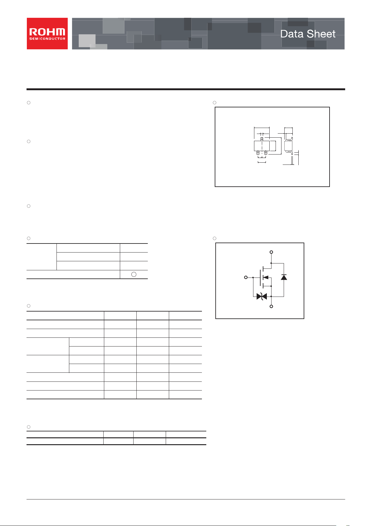
Structure Dimensions (Unit : mm)
Silicon N-channel
MOSFET transistor
Features
1) Low on-resistance.
2) High ESD.
3) High-speed switching.
4) Low-voltage drive (4V).
5) Drive circuits can be simple.
6) Parallel use is easy.
Applications
Switching
Packaging specifications Equivalent circuit
Package
Code
Type
RHU002N06
RHU002N06FRA
Basic ordering unit (pieces)
Taping
T106
3000
UMT3
(1) Source
(2) Gate
(3) Drain
(2)
2.0
0.3
(3)
(1)
(2)
0.65
0.65
1.3
Abbreviated symbol : KP
(3)
0.9
0.7
0.2
2.1
1.25
0.15
0.1Min.
Each lead has same dimensions
∗2
Absolute maximum ratings (Ta=25C)
Parameter
Drain-source voltage
Gate-source voltage
Drain current
Source current
(Body diode)
Continuous
Pulsed
Continuous
Pulsed
Total power dissipation
Channel temperature
Storage temperature
∗1 Pw≤10μs, Duty cycle≤1%
∗2 Each terminal mounted on a recommended
Symbol Limits Unit
V
DSS
V
GSS
D
∗1
I
DP
I
S
∗1
I
SP
∗2
P
D
Tch
Tstg °C
Thermal resistance
Parameter Symbol
Channel to ambient
∗
With each pin mounted on the recommended land.
Rth (ch-a)
∗
60 V
±20
±200I
200
800
200
150
−55 to +150
Limits
625
V
mA
mA±800
mA
mA
mW
°C
Unit
°C / W
∗1
(1)
Source
(2)
∗1 ESD PROTECTION DIODE
∗2 BODY DIODE
∗
A protection diode has been built in between the
gate and the source to protect against static
electricity when the product is in use.
Use the protection circuit when fixed voltages are
exceeded.
(1)
Gate
(3)
Drain
www.rohm.com
c
2012 ROHM Co., Ltd. All rights reserved.
○
1/3
2012.05 - Rev.C

Electrical characteristics (Ta=25C)
Parameter
Gate leakage current
Drain-source breakdown voltage
Drain cutoff current
Gate threshold voltage
Drain-source on-state resistance
Forward transfer admittance
Input capacitance
Output capacitance
Reverse transfer capacitance
Turn-on delay time
Rise time
Turn-off delay time
Fall time
Total gate charge
Gate-source charge
Gate-drain charge
∗ Pulsed
Body diode characteristics (Source-drain) (Ta=25C)
Parameter Symbol
Forward voltage
∗Pulsed
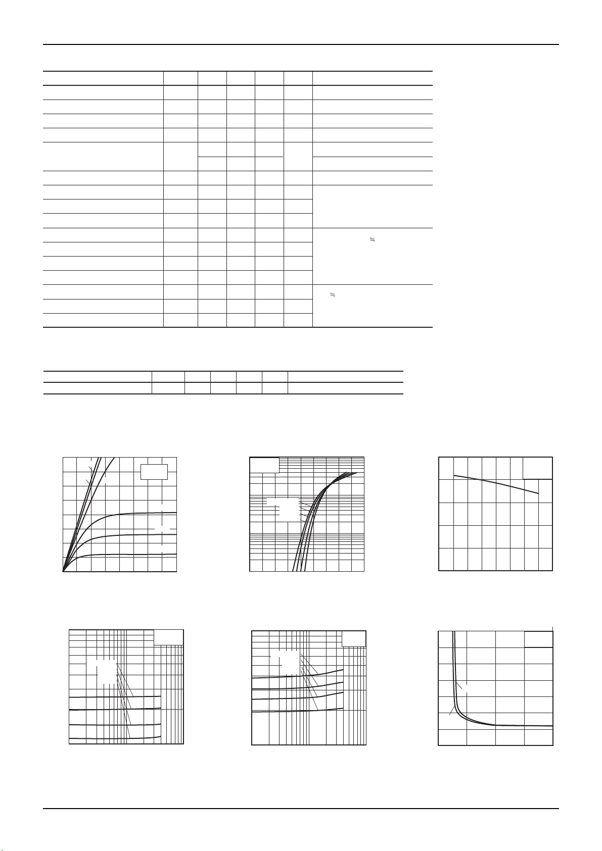
Electrical characteristic curves
0.8
10V
0.7
8V
0.6
(A)
D
0.5
0.4
0.3
0.2
DRAIN CURRENT : I
0.1
0.0
0.0 0.5 1.0 1.5 2.0 2.5 4.03.0 3.5
DRAIN-SOURCE VOLTAGE : V
Fig.1 Typical Output Characteristics
10
(Ω)
DS (on)
STATIC DRAIN-SOURCE
ON-STATE RESISTANCE : R
1.0
Fig.4 Static Drain-Source On-State
Resistance vs. Drain Current ( Ι )
6V
Ta=125°C
75°C
25°C
−25°C
0.1
DRAIN CURRENT : I
Ta=25°C
Pulsed
4V
3.5V
VGS=3V
DS
VGS=10V
Pulsed
D
(A)
Symbol
V
V
R
V
SD
(V)
I
GSS
(BR) DSS
I
DSS
GS (th)
DS (on)
l Yfs l
C
iss
oss
C
C
rss
t
d (on)
∗
t
r
t
d (off)
∗
t
f
∗
Q
g
Q
gs
Q
gd
∗
1.00.01
∗
∗
∗
∗
∗
Typ.
Min.
−
60
−
1
−
∗
−
0.1
−
−
−
−
−
−
−
Max.
±10
−
−
−
−
2.5
1.7
2.4
2.8 4.0
−
15
8
4
6
5
12
95
− 2.2 4.4
0.6
−
0.3
−
Min. Typ. Max.
−−1.2 V IS=200mA, VGS=0V
1
VDS=
10V
Pulsed
(A)
D
0.1
0.01
DRAIN CURRENT : I
0.001
GATE-SOURCE VOLTAGE : V
Fig.2 Typical Transfer Characteristics
10
(Ω)
DS (on)
STATIC DRAIN-SOURCE
ON-STATE RESISTANCE : R
1.0
Fig.5 Static Drain-Source On-State
Resistance vs. Drain Current ( ΙΙ )
Unit
μA
V
−
μA
1
V
Ω
S
−
pF
−
pF
−
pF
−
ns
−
ns
−
ns
−
ns
−
nC
nC
−
nC
−
Unit
Ta=−25˚C
25˚C
75˚C
125˚C
1.00.50.0
1.5 2.0 2.5
Ta=125°C
75°C
25°C
−25°C
0.1
DRAIN CURRENT : I
Test Conditions
V
GS
=±20V, VDS=0V
I
D
=1mA, VGS=0V
V
DS
=60V, VGS=0V
V
DS
=10V, ID=1mA
I
D
=200mA, VGS=10V
D
=200mA, VGS=4V
I
VDS=10V, ID=200mA
V
DS
=10V
VGS=0V
f=1MHz
D
=100mA, V
I
DD
30V
VGS=10V
RL=300Ω
R
G
=10Ω
VDD 30V
V
GS
=10V
I
D
=200mA
Conditions
3.0 3.5
4.54.0
GS
(V)
VGS=4V
Pulsed
1.00.01
D
(A)
Data Sheet RHU002N06FRA
2.5
(V)
GS (th)
2.0
1.5
1.0
0.5
GATE THRESHOLD VOLTAGE : V
0.0
CHANNEL TEMPERATURE : Tch
Fig.3 Gate Threshold Voltage
7
6
(Ω)
5
DS (on)
4
ID=200mA
3
2
100mA
1
ON-STATE RESISTANCE : R
STATIC DRAIN-SOURCE
0
0 5 10 15 20
GATE-SOURCE VOLTAGE : V
Fig.6 Static Drain-Source On-State
Resistance vs. Gate-Source Voltage
50 75 100 12525
vs. Channel Temperature
V
DS
=
10V
ID=1mA
Pulsed
(°C)
Ta=25°C
Pulsed
GS
(V)
150−50 −25 0
www.rohm.com
2/3
c
2012 ROHM Co., Ltd. All rights reserved.
○
2012.05 - Rev .C
 Loading...