ROHM DTA114YEB Schematic [ru]

Transistors DTA114YEB
z
z
z
z
z
z
z
-100mA / -50V Digital transistors
(with built-in resistors)
DTA114YEB
Applications
Inverter, Interface, Driver
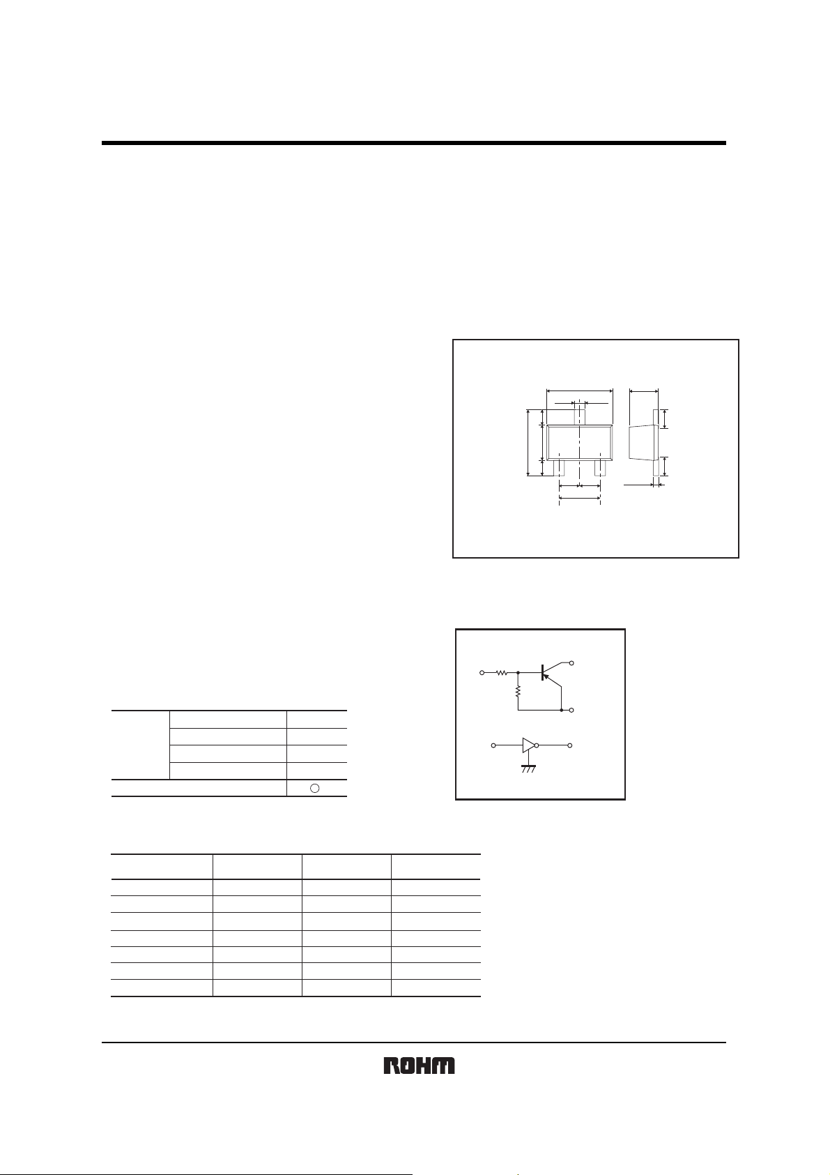
Dimensions (Unit : mm)
EMT3F
!!!!!!!!
z
Features
1)Built-in bias resistors enable the configuration of
an inverter circuit without connecting external
input resistors (see equivalent circuit).
2)The bias resistors consist of thin-film resistors
with complete isolation to allow negative biasing
of the input. They also have the advantage of
almost completely eliminating parasitic effects.
3)Only the on/off conditions need to be set for
operation, making the device design easy.
Structure
PNP silicon epitaxial planar transistor type
(Resistor built-in)
Packaging specifications
z
EMT3F
TL
3000
Part No.
DTA114YEB
Package
Packaging type Taping
Code
Basic ordering unit (pieces)
1.6
(1) IN
(2) GND
(3) OUT
Equivalent circuit
R
1
IN
R
2
IN
R1=10kΩ, R2=47kΩ
1.6
0.26
(3)
0.37
0.86
(1) (2)
0.37
0.5 0.5
1.0
Abbreviated symbol : 54
OUT
GND(+)
OUT
+)
GND(
0.7
0.45
0.13
Each lead has same dimensions
0.45
z
Absolute maximum ratings (T a=25qC)
Supply voltage
Input voltage
Collector current
Output current
Power dissipation
Junction temperature
Storage temperature
∗1 Characteristics of built-in transistor
∗2 Each terminal mounted on a recommended land
V
V
Io
P
Tj
Tstg
CC
IN
∗1
∗2
D
LimitsParameter Symbol
−50
−40 to +6
−100 mAIc(max)
−70
150
150
−55 to +150
Unit
V
V
mA
mW
°C
°C
1/2

Transistors DTA114YEB
z
z
Electrical characteristics (Ta=25qC)
Parameter Symbol
Input voltage
Output voltage
Input current
Output current
DC current gain
Transition frequency
Input resistance
Resistance ratio
∗ Characteristics of built-in transistor
z
Electrical characteristic curves
−100
−50
−20
(V)
I(on)
−10
−5
Ta=−40°C
25°C
−2
−1
−500m
INPUT VOLTAGE : V
−200m
−100m
−100μ
100°C
−1m
−200μ
−2m −20m−500μ−5m −50m
OUTPUT CURRENT : I
−10m
O
(A)
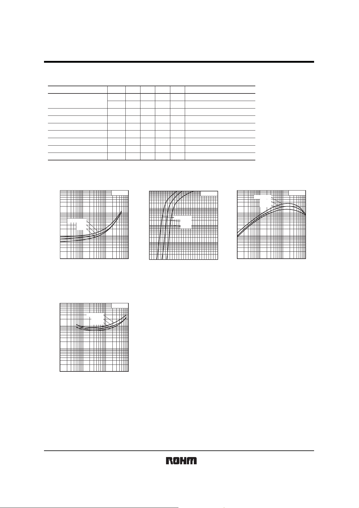
Fig.1 Input voltage vs. output current
(ON characteristics)
V
I(off)
V
I(on)
V
O(on)
I
I
I
O(off)
G
I
f
T
R
1
R2/R
1
VO=−0.3V
Min.
Typ. Max. Unit Conditions
−300
−
−
−1.4
−100
−
−
−
68
−
7
3.7
−10m
(A)
−500μ
−200μ
−100μ
OUTPUT CURRENT : Io
−100m
−
−
−
−
250
10
4.7
−5m
−2m
−1m
−50μ
−20μ
−10μ
−5μ
−2μ
−1μ
0 −3.0
mV
−
V
−300
mV
−880
μA
−500
nA
−
−
−
MHz
13
kΩ
5.7
−−
Ta=100°C
25°C
−40°C
−0.5 −1.0 −1.5 −2.0 −2.5
INPUT VOLTAGE : V
Fig.2 Output current vs. input voltage
(OFF characteristics)
V
CC
=−5V, IO=−100μA
V
O
=−0.3V, IO=−1mA
I
O/II
=−5mA/−0.25mA
V
I
=−5V
V
CC
=−50V, VI=0V
O
=−5V, IO=−5mA
V
CE
=−10V, IE=5mA, f=100MHz∗
V
V
CC
=−
I(off)
(V)
−
5V
I
DC CURRENT GAIN : G
1k
500
200
100
50
20
10
5
2
1
−100μ−1m −10m −100m
Ta=100°C
25°C
−40°C
−200μ−2m −20m−500μ−5m −50m
OUTPUT CURRENT : I
O
(A)
VO=−5V
Fig.3 DC current gain vs. output
current
!!!!!!!!
−1
−500m
(V)
−200m
O(on)
−100m
−50m
−20m
−10m
−5m
OUTPUT VOLTAGE : V
−2m
−1m
−100μ
−200μ
Ta=100°C
25°C
−40°C
−1m
−2m −20m−500μ−5m −50m
−10m
OUTPUT CURRENT : I
Fig.4 Output voltage vs. output
current
O
lO/lI=20
−100m
(A)
2/2
 Loading...