ROHM BU9910KV Datasheet

•
Applications
PCs
1
Multimedia ICs
Status display LCD driver for PCs
with I2C Bus interface
BU9910KV
The BU9910KV is a status LCD driver with I2C Bus intetface. Various lighting mode can be controlled through I2C
Bus. In addition, 20 direct drive inputs allow the application to drive 20 elements directly without I
2
C Bus, so that the
system configuration can be kept simple.
•
Features
1) I
2
C Bus interface.
2) Drive up to 44 LCD cells.
4 common × 11 segment, 1 / 3 bias, 1 / 4 duty
3) Blink operation for eaeh cell.
4) Support four frame frequencies
256Hz, 128Hz, 64Hz, 32Hz (at f
OSC = 32.768kHz)
5) 20 direct drive inputs, which allow the application to
drive LCD directly without I
2
C control.
6) Minimum LCD drive time is guaranteed for direct in.
7) LCD device test ferminals.(LCDT0, LCDT1)
8)Power aupply voltages: 3.3V to 5.0V

2
Multimedia ICs BU9910KV
•
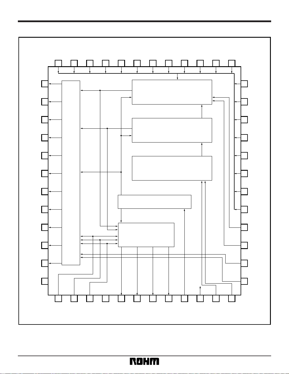
Block diagram
36
37SEG10
SEG9
SEG8
SEG7
SEG6
SEG5
SEG4
SEG3
SEG2
SEG1
SEG0
V
DD
38
39
40
41
42
43
44
45
46
47
48
24 DIN7
DIN6
DIN5
DIN4
DIN3
DIN2
DIN1
DIN0
HT1
HT0
LCDT1
LCDT0
23
22
21
20
19
18
17
16
15
14
13
35 34 33 32 31 30 29 28 27 26 25
121110987654321
VL2
VL1
GND
COM3
COM2
COM1
COM0
CLK
#RES
SDA
SCL
VL3
DIN18
DIN17
DIN16
DIN15
DIN14
DIN13
DIN12
DIN11
DIN10
DIN9
DIN8
DIN19
Timing Generator
Date Latch Logic
Control Logic
I2CBus
Interface
Common
Driver
Segment
Driver

3
Multimedia ICs BU9910KV
•
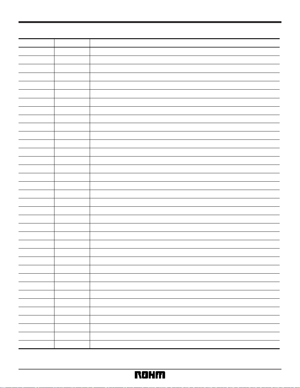
Pin descriptions
Pin No. Pin name Function
1
2
3
4
5
6
7
8
9
10
11
12
13
14
15
16
17
18
19
20
21
22
23
24
25
26
27
28
29
30
31
32
33
34
35
36
VL3
VL2
VL1
GND
COM3
COM2
COM1
COM0
CLK
#RES
SDA
SCL
LCDT0
LCDT1
HT0
HT1
DIN0
DIN1
DIN2
DIN3
DIN4
DIN5
DIN6
DIN7
DIN8
DIN9
DIN10
DIN11
DIN12
DIN13
DIN14
DIN15
DIN16
DIN17
DIN18
DIN19
Input for LCD driver
Input for LCD driver (2 / 3)
∗VL3
Input for LCD driver (1 / 3)
∗VL3
Ground
LCD common driver output 3
LCD common driver output 2
LCD common driver output 1
LCD common driver output 0
Clock input (ex.32.768kHz)
Reset
I
2
CBus Serial Data Line
I
2
CBus Serial Clock Input
LCD Device test mode set 0
LCD Device test mode set 1
Direct IN Hold time set 0
Direct IN Hold time set 1
Direct IN 0
Direct IN 1
Direct IN 2
Direct IN 3
Direct IN 4
Direct IN 5
Direct IN 6
Direct IN 7
Direct IN 8
Direct IN 9
Direct IN 10
Direct IN 11
Direct IN 12
Direct IN 13
Direct IN 14
Direct IN 15
Direct IN 16
Direct IN 17
Direct IN 18
Direct IN 19

4
Multimedia ICs BU9910KV
Pin No. Pin name Function
37
38
39
40
41
42
43
44
45
46
47
48
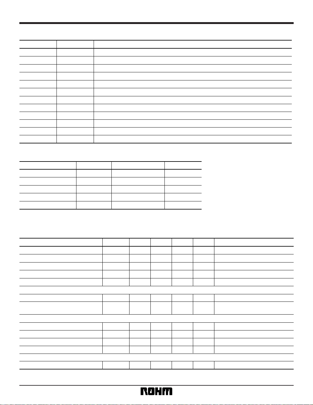
SEG10
SEG9
SEG8
SEG7
SEG6
SEG5
SEG4
SEG3
SEG2
SEG1
SEG0
V
DD
LCD segment driver output 10
LCD segment driver output 9
LCD segment driver output 8
LCD segment driver output 7
LCD segment driver output 6
LCD segment driver output 5
LCD segment driver output 4
LCD segment driver output 3
LCD segment driver output 2
LCD segment driver output 1
LCD segment driver output 0
Supply Voltage 3.0V to 5.5V
•
Absolute maximum ratings (Ta = 25°C)
Parameter Symbol Limits Unit
Applied voltage
Power dissipation
Operating temperature
Storage temperature
Input voltage
V
DD
Pd
Topr
Tstg
V
IN
7.0
400
∗
GND – 0.5 ~ VDD + 0.5
V
mW
°C
°C
V
∗
Reduced by 4mW for each increase in Ta of 1°C over 25°C.
䊊 ROHM holds a license from Philips semicondoctors for the “I
2
C Bus.”
– 15 ~ + 75
– 55 ~ + 125
•
Electrical characteristics (unless otherwise noted, Ta = 25°C, VDD = 5.0V)
Parameter
Symbol Min. Typ. Max. Unit Conditions
Circuit current
Input high level voltage
Input low level voltage
Input high level current
Input low level current
〈SDA pin〉
Output low level voltage
Output fall time
〈COM, SEG pins〉
Output intermediate level voltage VL3
Output intermediate level voltage VL2
Output intermediate level voltage VL1
Output low level voltage
〈LCDT pin〉
Pull-up resistance
I
DD
V
IH
V
IL
I
IH
I
IL
VOLsda
tfsda
V
OM3
V
OM2
V
OM1
V
OL
R
PU
20
VDD∗0.7
–
0.5
—
–
1.0
0.0
—
VL3 – 0.1
VL2 – 0.1
VL1 – 0.1
0.0
24k
35
V
DD
0.0
0.0
0.0
0.2
—
VL3
VL2
VL1
0.2
30k
50
V
DD
+ 0.5
V
DD
∗
0.3
1.0
—
0.6
250
VL3 + 0.1
VL2 + 0.1
VL1 + 0.1
0.6
36k
µA
V
V
µA
µA
V
ns
V
V
V
V
Ω
—
—
—
—
—
Bias 51kΩ × 3
I
OL
= 6.0mA
CL = 400pF
I
OL
= 6.0mA
I
OM3
= 100µA
I
OM2
= 100µA
I
OM1
= 100µA
I
OL
= 100µA
䊊 Not designed for radiation resistance.

5
Multimedia ICs BU9910KV
•
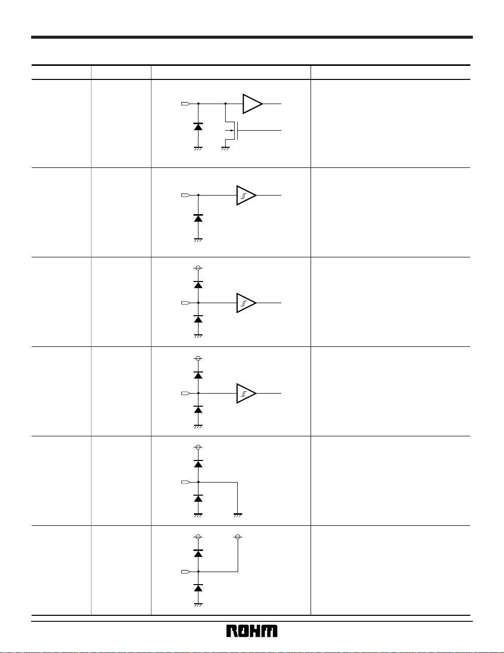
Input / output circuits
Pin No. Pin name Equivalent circuit Pin description
11
12
9
10
4
48
SDA
SCL
CLK
#RES
GND
V
DD
I2C Bus serial data input / output.
I
2
C Bus serial clock Input.
Clock Input for LCD display.
Clock frequency is 32.768kHz.
Reset input.(Low Active)
Low: Reset all internal registers.
Note: Require external power on reset.
Power supply.
3.0V to 5.5V supply voltage range.
Ground terminal.
 Loading...