

Page 1
Memory for Plug & Play
EDID Memory
(For display)
BR24C21,BR24C21F,BR24C21FJ,BR24C21FV,
BU9882-W,BU9882F-W,BU9882FV-W
BR24C21,BR24C21F,BR24C21FJ,BR24C21FV
●Description
BR24C21F,BR24C21FJ,BR24C21FV are serial EEPROMs that support DDC1
for Plug and Play displays.
●Features
1) Compatible with both DDC1
2) Operating voltage range: 2.5V to 5.5V
3) Page write function: 8bytes
4) Low power consumption
Active (at 5V) : 1.5mA (typ)
Stand-by (at 5V) : 0.1µA (typ)
5) Address auto increment function during Read operation
6) Data security
Write enable feature (VCLK)
Write protection at low Vcc
7) Various packages available: DIP-T8(BR24C21) / SOP8(BR24C21F) / SOP-J8(BR24C21FJ) / SSOP-B8(BR24C21FV)
8) Initial data=FFh
9) Data retention: 10years
10) Rewriting possible up to 100,000 times
●Absolute maximum ratings (Ta=25℃)
Parameter Symbol Rating Unit
Supply Voltage VCC -0.3~+6.5 V
Power Dissipation Pd
Storage Temperature
Operating Temperature
Terminal Voltage
* Reduce by 8.0 mW/C over 25C (*1), 4.5mW/℃ (*2,3), and 3.5mW/℃ (*4)
●Memory cell characteristics
Parameter Symbol Rating Unit
Supply Voltage VCC 2.5~5.5 V
Input Voltage VIN 0~VCC V
●Recommended operating conditions
Parameter
Write/Erase Cycle 100,000 - - Cycle
Data Retention 10 - - Year
TM
/DDC2TM
800 (DIP-T8)
450 (SOP8)
450 (SOP-J8)
350 (SSOP-B8)
Tst g - 65 ~+125 ℃
Topr -40~+85 ℃
- -0.3~VCC+0.3 V
Limits
Min. Typ. Max.
TM
*1
*2
*3
*4
Unit
/DDC2
mW
TM
interfaces
No.11002ECT02
www.rohm.com
1/22
© 2011 ROHM Co., Ltd. All rights reserved.
2011.08 - Rev.C
Page 2
BR24C21,BR24C21F,BR24C21FJ,BR24C21FV,
BU9882-W,BU9882F-W,BU9882FV-W
Technical Note
●Electrical characteristics - DC (Unless otherwise specified, Ta=-40℃~+85℃、VCC=2.5V~5.5V)
Parameter Symbol
Min. Typ. Max.
Limits
Unit Condition
“H” Input Voltage 1 VIH1 0.7VCC - - V SCL, SDA
“L” Input Voltage 1 VIL1 - - 0.3VCC V SCL, SDA
“H” Input Voltage 2 VIH2 2.0 - - V VCLK
“L” Input Voltage 2 VIL2 - - 0.8 V VCLK, VCC≧4.0V
“L” Input Voltage 3 VIL3 - - 0.2VCC V VCLK, VCC<4.0V
“L” Output Voltage VOL - - 0.4 V SDA, IOL=3.0mA
Input Leakage Current ILI -1 - 1 µA SCL, VCLK, VIN=0V~VCC
Output Leakage Current ILO -1 - 1 µA SDA, VOUT=0V~VCC
Operating Current ICC - - 3.0 mA VCC=5.5V, fSCL=400kHz
Standby Current ISB - 10 100 µA VCC=5.5V, SDA=SCL=VCC,VCLK=GND *1
Note: This IC is not designed to be radiation-resistant
*1 Transmit-Only Mode - After power on, the BR24C21/F/FJ/FV is in Standby mode and does not provide the clock to the VCLK pin.
After the clock is provided to VCLK, the device is switched from Standby to Transmit-Only Mode, and the operating current flows.
Bi-directional Mode - The BR24C21/F/FJ/FV is in Standby mode after each command is performed.
●Electrical characteristics - AC (Unless otherwise specified, Ta=-40℃~+85℃,V
Fast-mode
CC=2.5V~5.5V
Parameter Symbol
V
CC=2.5V~5.5V)
Standard-mode
VCC=2.5V~5.5V
Unit
Min. Typ. Max. Min. Typ. Max.
Clock Frequency fSCL - - 400 - - 100 kHz
Data Clock High Period tHIGH 0.6 - - 4.0 - -
Data Clock Low Period tLOW 1.3 - - 4.7 - - µs
SDA and SCL Rise Time tR - - 0.3 - - 1.0 µs
SDA and SCL Fall Time tF - - 0.3 - - 0.3 µs
Start Condition Hold Time tHD:STA 0.6 - - 4.0 - - µs
Start Condition Setup Time tSU:STA 0.6 - - 4.7 - - µs
Input Data Hold Time tHD:DAT 0 - - 0 - - ns
Input Data Setup Time tSU:DAT 100 - - 250 - - ns
Output Data Delay Time(SCL) tPD - - 0.9 - - 3.5 µs
Stop Condition Setup Time tSU:STO 0.6 - - 4.0 - - µs
Bus Free Time tBUF 1.3 - - 4.7 - - µs
Write Cycle Time tWR - - 10 - - 10 ms
Noise Spike Width (SDA and SCL) tI - - 0.1 - - 0.1 µs
AC OPERATING CHARACTERISTICS (Transmit-Only Mode)
Output Data Delay Time(VCLK) tVPD - - 1.0 - - 2.0 µs
VCLK High Period tVHIGH 0.6 - - 4.0 - - µs
VCLK Low Period tVLOW 1.3 - - 4.7 - - µs
VCLK Setup Time tVSU 0 - - 0 - - µs
VCLK Hold Time tVHD 0.6 - - 4.0 - - µs
Mode Transition Time tVHZ - - 0.5 - - 1.0 µs
Transmit-Only Powerup Time tVPU 0 - - 0 - - µs
Noise Spike Width (VCLK) tVI - - 0.1 - - 0.1 µs
µs
www.rohm.com
2/22
© 2011 ROHM Co., Ltd. All rights reserved.
2011.08 - Rev.C
Page 3
BR24C21,BR24C21F,BR24C21FJ,BR24C21FV,
BU9882-W,BU9882F-W,BU9882FV-W
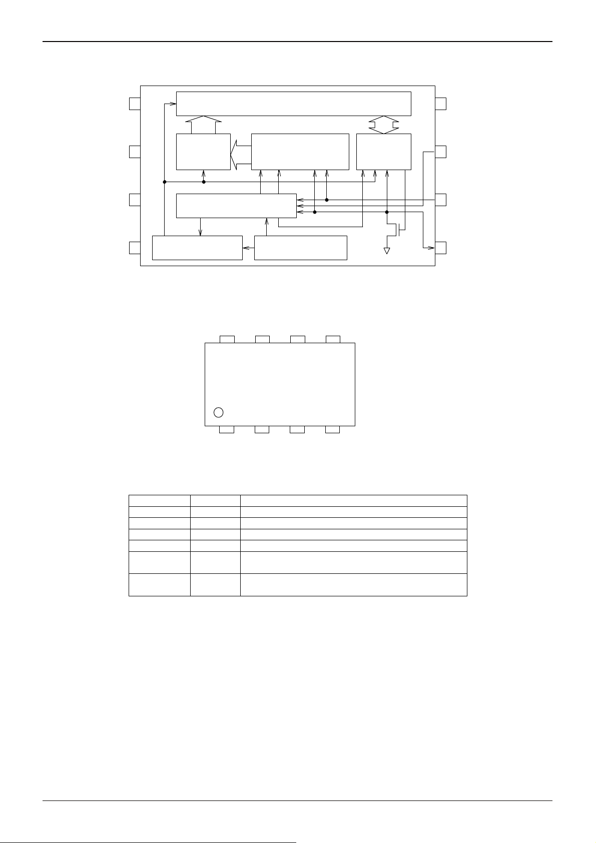
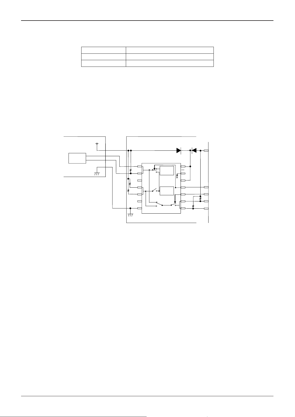
●Block diagram
1
N.C.
1 Kbit EEPROM ARRAY
Technical Note
8
VCC
N.C.
N.C.
GND
●Pin layout diagram
7bit
2
3
ADDRESS
DECODER
CONTROL LOGIC
HIGH VOLTAGE VCC LEVEL DETECT
7bit
START STOP
SLAVE・WORD
ADDRESS REGISTER
DATA
REGISTER
ACK
Fig.1 Block Diagram
VCC VCLK
(
入力)
BR24C21
SCL SDA
BR24C21F
BR24C21FJ
BR24C21FV
N.C.
N.C.
GND N.C.
Fig.2 Pin Layout
Pin Name I/O Functions
VCC - Power Supply
GND - Ground (0V)
N.C. - No Connection
SCL IN Serial Clock Input for Bi-directional Mode
SDA IN/OUT
VCLK IN
*1 An open drain output requires a pull-up resistor.
Slave and Word Address,
Serial Data Input, Serial Data Output
Clock Input (Transmit-Only Mode)
Write Enable (Bi-directional Mode)
8bit
7
VCLK
6
SCL
5 4
SDA
*1
www.rohm.com
3/22
© 2011 ROHM Co., Ltd. All rights reserved.
2011.08 - Rev.C
Page 4
BR24C21,BR24C21F,BR24C21FJ,BR24C21FV,
A
BU9882-W,BU9882F-W,BU9882FV-W
Technical Note
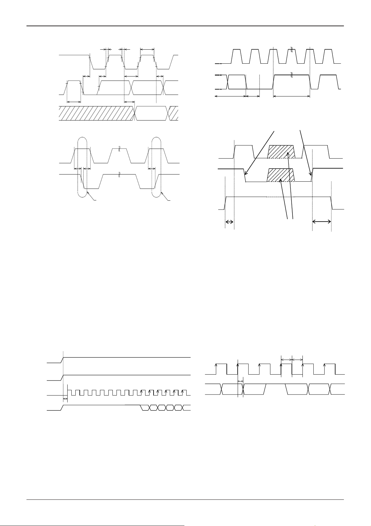
●Synchronous data timing
t
tR tF
HIGH
SCL
SDA
(IN)
SDA
(OUT)
tHD:STA
t
t
BUF
t
SU
:DAT
t
LOW
PD
t
HD
:DAT
SCL
SD
D0 ACK
WRITE DATA(n)
tWR
STOP CONDI TI ON START CONDI TION
Fig.4 Write Cycle Timing
START BIT
STOP BIT
SCL
tSU:STA
SDA
tHD:STA
Fig.3 Synchronous Data Timing
START BIT
t
SU:STO
STOP BIT
SCL
SDA
VCLK
・SDA data is latched into the chip at the rising edge of the SCL clock.
・Output data toggles at the falling edge of the SCL clock.
t
VSU
Fig.5 Write Enable Timing
WRITE COMMAND
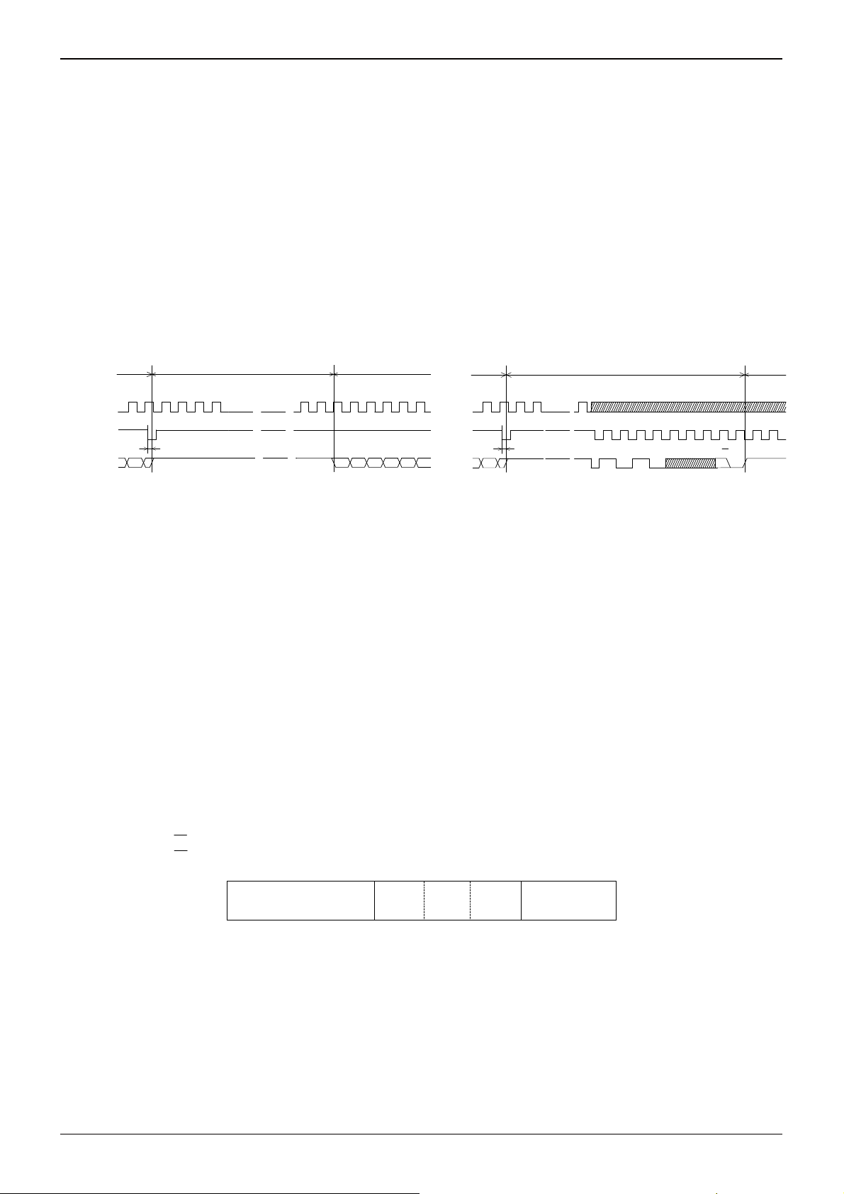
●Transmit-only mode
・After power is on, the BR24C21/F/FJ/FV is in Transmit-Only Mode. In this mode data can be output by providing the clock
to the VCLK pin.
・When the power is on, the SCL pin needs to be set to VCC(High level).
・SDA is at high-impedance during input of the first 9 clocks. At the 10th rising clock edge of VCLK data is output. After
power on, the output data is as follows:
00h address data → 01h address data → 02h address data →
…
The address is incremented by one, after every 9 clocks of VCLK. All addresses are output in this mode.
When the counter reaches the last address, the next output data is 00h address data. (See Fig. 6)
・In this mode, the NULL bit (High data) is output between the address data and the next address data. (See Fig. 7)
・The read operation is in Transmit-Only Mode and can be started after the power is stabilized.
Vcc
SCL
VCLK
tVPU
SDA
Fig.6 Transmit Only Mode
9
101
D7 D6 D5 D4 D3
00h ADDRESS DATA
VCLK
SDA
tVPD
ADDRESS n
DATA
D0D1 D7 D6
Fig.7 Null Bit
NULL BIT
DATA=1
tVHIGH tVLOW
ADDRESS n+1
DATA
t
VHD
www.rohm.com
4/22
© 2011 ROHM Co., Ltd. All rights reserved.
2011.08 - Rev.C
Page 5
BR24C21,BR24C21F,BR24C21FJ,BR24C21FV,
BU9882-W,BU9882F-W,BU9882FV-W
Technical Note
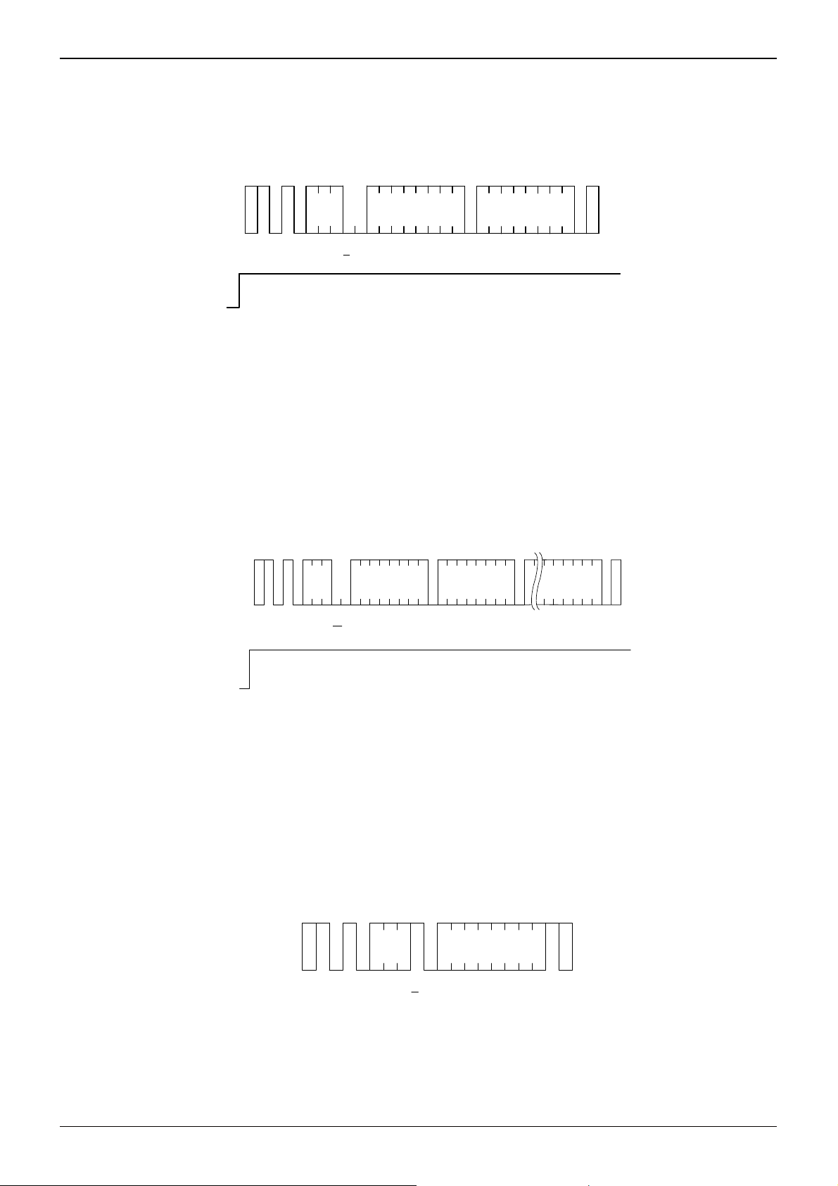
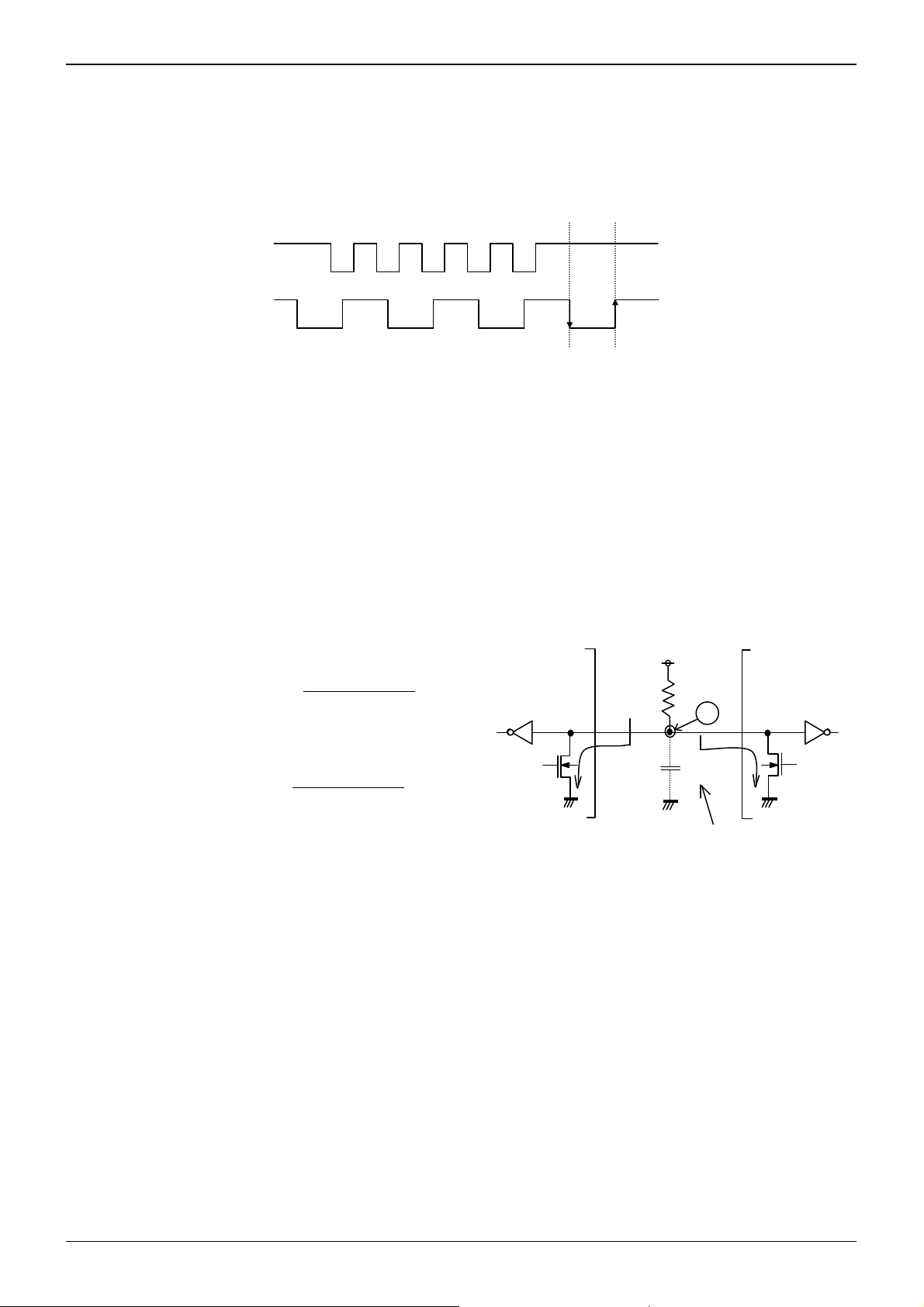
●Bi-directional mode
○Bi-directional Mode and Recovery Function
・The BR24C21/F/FJ/FV can be switched from Transmit-Only Mode to Bi-directional Mode by providing a valid High to Low
transition at the SCL pin, while the state of SDA is at high-impedance.
・After a valid high to low transition on the SCL pin, the BR24C21/F/FJ/FV begins to count the VCLK clock. If the VCLK
counter reaches 128 clocks without the command for Bi-directional Mode, the device reverts to Transmit-Only Mode
(Recovery function). The VCLK counter is reset by providing a valid high to low transition at the SCL pin. After reversal
to Transmit-Only Mode the device begins to output data (00h address data) with the 129th rising clock edge of VCLK.
・If the BR24C21/F/FJ/FV is switched from Transmit-Only Mode and receives the command for Bi-directional
Mode and responds with an Acknowledge, it is impossible to revert to Transmit-Only Mode. (Power down
way to revert to Transmit-Only Mode.) Unless the input device code is “1010”, the device does
Acknowledge. If the VCLK counter reaches 128 clocks afterwards, it is possible to revert
not respond with an
to Transmit-Only Mode for
is the only
Recovery function. If the Master generates a STOP condition during the Slave address, before an Acknowledge is input,
it is possible to revert to Transmit-Only Mode.
・When the device is switched from Transmit-Only Mode to Bi-direction Mode, the period of tVHZ needs to be held.
MODE
VCLK
SCL
SDA
Transmit-only
Trans mit -on ly
Bi-directional
Bi-directional
Transition Mode with possibility
Transition Mode with possibility to
to retune to Transmit-Only Mode
return to Transmit-Only Mode
21
3 4
tVHZ
Fig.8 Recovery Mode
127
128
129
Transmit-Only
Transmit-Only
ADDRESS 00h
ADDRESS 00h
D7
D6D5D4
MODE
VCLK
SCL
SDA
Transmit-oOnly
Trans mit -on ly
tVHZ
Bi-directional
Bi-directional
Transition Mode with possibility
Transition Mode with possibility to
to retune to Transmit-Only Mode
return to Transmit-Only Mode
n<128
21n
10 1 ***0
Fig.9 Mode Change
○Bi-directional Mode
START Condition
・All commands are proceeded by the START condition, which is a High to Low transition of SDA when SCL is High.
・The BR24C21/F/FJ/FV continuously monitors the SDA and SCL lines for the START condition and will not respond to
any commands until this condition has been met.
(See Fig. 3 Synchronous Data Timing)
STOP Condition
・All commands must be terminated by a STOP condition, which is a Low to High transition of SDA when SCL is High.
・The STOP condition causes the internal write cycle to write data into the memory array after a write sequence.
・The STOP condition is also used to place the device into standby power mode after read sequences.
・A STOP condition can only be issued after the transmitting device has released the bus.
(See Fig.3 Synchronous Data Timing)
Device Addressing
・Following the START condition, the Master outputs the device address of the Slave to be accessed. The most
significant four bits of Slave address are the “device type indentifier,” For the BR24C21/F/FJ/FV this is fixed as
“1010.”
・The next three bits of the slave address are inconsequential.
・The last bit of the stream determines the operation to be performed. When set to “1”, a READ operation is selected.
When set to “0”, a WRITE operation is initiated.
R/W set to "0"
R/W set to "1"
・ ・ ・ ・ ・ ・ ・ ・ WRITE (This bit is also set to "0" for random read operation)
・ ・ ・ ・ ・ ・ ・ ・ READ
1010
* * *
_
R/W
*:Don’t care
○Write Protect Function
・Write Enable (VCLK)
When using the BR24C21/F/FJ/FV in Bi-directional Mode, the VCLK pin can be used as a write enable pin. Setting
VCLK High allows normal write operations, while setting VCLK low prevents writing to any location in the array.
(See Fig.5 Write Enable Timing)
Changing VCLK from High to Low during the self-timed program operation will not halt programming of the device.
Bi-directional
parmanently
ACK
R/WS
*Don’t care
Bi-directional
parmanently
www.rohm.com
5/22
© 2011 ROHM Co., Ltd. All rights reserved.
2011.08 - Rev.C
Page 6
BR24C21,BR24C21F,BR24C21FJ,BR24C21FV,
S
R
S
P
S
E
S
R
S
)
E
)
BU9882-W,BU9882F-W,BU9882FV-W
●Bidirectional mode command
○Byte Write
When the Master generates a STOP condition, the BR24C21/F/FJ/FV begins the internal write cycle to the nonvolatile array.
DA
LINE
VCLK
T
A
SLAVE
R
ADDRESS
T
○Page Write
If the Master transmits the next data instead of generating a STOP condition during the byte write cycle, the
BR24C21/F/FJ/FV transfers from byte write function to page write function. After receipt of each word, the three lower
order address bits are internally incremented by one, while the high order four bits of the word address remains
constant.
If the master transmits more than eight words, prior to generating the STOP condition, the address counter will “roll
over,” and the previous transmitted data will be overwritten.
SDA
LINE
T
A
R
T
1
SLAV
ADDRESS
1
0 0
VCLK
○Current Read
The BR24C21/F/FJ/FV contains an internal address counter which maintains the address of the last word accessed,
incremented by one. If the last accessed address is address “n” in a Read operation, the next Read operation will
access data from address “n+1” and increment the current address counter. If the last accessed address is address
”n” in a Write operation, the next Read operation will access data from address “n”. If the Master does not transfer an
Acknowledge, but does generate a STOP condition, the current address read operation will only provide a single byte of
At this point, the device discontinues transmission.
data.
(See Fig.14 Sequential Read Cycle Timing)
SDA
LINE
S
T
A
R
T
W
R
I
T
E
* *
*
WORD
ADDRESS
WA
*
6
WA
D7 1 1 0 0
0
A
C
/
K
W
A
C
K
Fig.10 Byte Write Cycle Timing
W
R
I
T
*
* *
W
WORD
ADDRESS
WA
*
6
A
/
C
K
WA
0
DATA(n
A
C
K
Fig.11 Page Write Cycle Timing
R
SLAVE
ADRESS
E
A
D
* *
*
A
R
C
/
K
W
DATA
D7 1 1 0 0
*:Don’tcare
Fig.12 Current Read Cycle Timing
DATA
D0
D7 D0
A
C
K
D0
*:Don’t care
DATA(n +7
*:Don’t care
S
T
O
P
D0
A
C
K
Technical Note
T
O
A
C
K
T
O
P
A
C
K
www.rohm.com
6/22
© 2011 ROHM Co., Ltd. All rights reserved.
2011.08 - Rev.C
Page 7

BR24C21,BR24C21F,BR24C21FJ,BR24C21FV,
BU9882-W,BU9882F-W,BU9882FV-W
○Random Read
The Random read operation allows the Master to access any memory location. This operation involves a two-step
process. First, the Master issues a Write command that includes the START condition and the Slave address field
(with R/W set to “0”) followed by the word address of the word to be read. This procedure sets the internal address
counter of the BR24C21/F/FJ/FV to the desired address. After the word address Acknowledge is received by the
Master, the Master immediately re-issues a START condition followed by the Slave address field with R/W set to “1.”
The device will respond with an Acknowledge and then transmit the 8-data bits stored at the addressed location. If the
Master does not acknowledge the transmission but does generate the STOP condition, the IC will discontinue
transmission.
SDA
LINE
S
T
A
R
T
10 0
SLAVE
ADDRESS
1* * *
W
R
I
T
E
R
/
W
Fig.13 Random Read Cycle Timing
○Sequential Read
・If the Master does not transfer an Acknowledge and does not generate a STOP condition during the current Read
operation, the BR24C21/F/FJ/FV continues to output the next address data in sequence. For Read operations, all bits
in the address counter are incremented, allowing the entire array to be read during a single operation. When the
counter reaches the top of the array, it will “roll over” to the bottom of the array and continue to transmit data.
・If the Master does not acknowledge the transmission but does generate a STOP condition, at this point the device
discontinues transmission.
・The sequential Read operation can be performed with both Current Read and Random Read.
SDA
LINE
S
T
A
SLAVE
R
ADDRESS
T
10 0
R
E
A
D
1* * * D0 D7 D0 D7
R
/
W
Fig.14 Sequential Read Cycle Timing
*
A
C
K
A
C
K
WORD
ADDRESS(n)
WA
6
DATA(n)
(Current Read)
WA
0
S
T
A
R
T
A
C
K
A
C
K
SLAVE
ADDRESS
10 01* *
R
E
A
D
*
D0
R
/
W
DATA(n)
D7
A
C
K
DATA(n+x)
A
C
K
*:Don’t care
*:Don’t care
Technical Note
S
T
O
P
A
C
K
S
T
O
P
A
C
K
www.rohm.com
7/22
© 2011 ROHM Co., Ltd. All rights reserved.
2011.08 - Rev.C
Page 8

BR24C21,BR24C21F,BR24C21FJ,BR24C21FV,
BU9882-W,BU9882F-W,BU9882FV-W
BU9882-W,BU9882F-W,BU9882FV-W
●Description
BU9882F-W,BU9882FV-W are dual port EEPROMs compatible with the DDC2
2 EDID channels to be read simultaneously.
●Features
1) Designed for use with DDC2
TM
2) 2-port simultaneous read function
3) Operating voltage range: 2.5V-5.5V
4) Page write function: 8bytes
5) Low power consumption:
Active
(at 5V) : 1.5mA(typ)
Stand-by (at 5V) : 0.1µA(typ)
6) Data security
Write protection with WP
Write protection at low power supply voltage
7) Various package types available: DIP14(BU9882-W) / SOP14(BU9882F-W) / SSOP14(BU9882FV-W)
8) Initial data: FFh
9) Data retention: 10years
10) Rewriting possible up to 100,000 times
●Absolute maximum ratings
Parameter Symbol Rating Unit
Supply Voltage VCC -0.3~+6.5 V
950 (DIP14)
Power Dissipation Pd
350 (SSOP14)
Storage Temperature
Operating
Temperature
Terminal Voltage
* Reduce by 9.5 mW/C over 25C (*1), 4.5mW/℃(*2), 3.5mW/℃(*3).
*4 6.8V (Max.)
Tst g - 65
Topr -40
- -0.3
~VCC+1.0
~+125 ℃
~+85 ℃
*1
*2
mW 450 (SOP14)
*3
*4
●Recommended operating conditions
Parameter Symbol Rating Unit
V
TM
. 2 independent ports allow
Technical Note
Supply Voltage VCC 2.5~5.5 V
Input Voltage VIN 0~VCC+1.0 V
●Memory cell characteristics
Parameter
Write/Erase Cycle
Min. Typ. Max.
100,000 - - Cycle
Limits
Data Retention 10 - - Year
www.rohm.com
8/22
© 2011 ROHM Co., Ltd. All rights reserved.
Unit
2011.08 - Rev.C
Page 9
BR24C21,BR24C21F,BR24C21FJ,BR24C21FV,
BU9882-W,BU9882F-W,BU9882FV-W
Technical Note
●Electrical characteristics – DC (Unless otherwise specified, Ta=-40℃~+85℃,VCC=2.5V~5.5V)
Parameter Symbol
“H” Input Voltage 1
“L” Input Voltage 1
VIH1 2.0 - - V
VIL1 - - 0.8 V V
Min. Typ. Max.
Limits
Unit Condition
CC≧4.0V
“L” Input Voltage 2 VIL2 - - 0.2VCC V VCC<4.0V
“L” output Voltage VOL1 - - 0.4 V SDA_PC0/1, IOL=3.0mA *1
Input Leakage Current 1 ILI1 -1 - 1 µA
Input Leakage Current 2 ILI2 -1 - 50 µA
Output Leakage Current ILO -1 - 1 µA
Operating Current ICC - 1.5 3.0 mA
Standby Current ISB - 0.1 5 µA
Note: This IC is not designed to be radiation-resistant
*1 IOL at monitor mode (DDCENA
at SDA_PC0/PC1
=HIGH) is the sum of current flowing from the pull up resistor at the SDA_MON side to the pull up resistance
SCL_PC0/1,DDCENA, BANKSEL,
VIN=0V
___
~VCC+1.0
WP
SDA_PC0/1,SCL/SDA_MON(DDCENA=GND),
VOUT=0V
fSCL=400kHz, V
~VCC+1.0
CC=5.5V
tWR=10ms
SCL/SDA_PC0/1=V
CC
SCL/SDA_MON=H-Z
DDCENA=WPB=BANKSEL=GND
DUALPCB=V
CC
●Electrical characteristics – AC (Unless otherwise specified, Ta=-40℃~+85℃、VCC=2.5V~5.5V)
Fast-mode
CC=2.5V~5.5V
Parameter Symbol
V
Min. Typ. Max. Min. Typ. Max.
Standard-mode
VCC=2.5V~5.5V
Unit
Typ.
Clock Frequency fSCL - - 400 - - 100 kHz
Data Clock High Period tHIGH 0.6 - - 4.0 - - µs
Data Clock Low Period tLOW 1.3 - - 4.7 - - µs
SDA and SCL Rise Time tR - - 0.3 - - 1.0 µs
SDA and SCL Fall Time tF - - 0.3 - - 0.3 µs
Start Condition Hold Time tHD:STA 0.6 - - 4.0 - - µs
Start Condition Setup Time tSU:STA 0.6 - - 4.7 - - µs
Input Data Hold Time tHD:DAT 0 - - 0 - - ns
Input Data Setup Time tSU:DAT 100 - - 250 - - ns
Output Data Delay Time(SCL) tPD - - 0.9 - - 3.5 µs
Stop Condition Setup Time tSU:STO 0.6 - - 4.0 - - µs
Bus Free Time tBUF 1.3 - - 4.7 - - µs
Write Cycle Time tWR - - 10 - - 10 ms
Noise Spike Width (SDA and SCL) tI - - 0.1 - - 0.1 µs
www.rohm.com
9/22
© 2011 ROHM Co., Ltd. All rights reserved.
2011.08 - Rev.C
Page 10

BR24C21,BR24C21F,BR24C21FJ,BR24C21FV,
BU9882-W,BU9882F-W,BU9882FV-W
●Block diagram
●Pin layout diagram
VCC WP DUALPCB BANKSEL DDCENA SCL_MON SDA_MON
Technical Note
1Kbit
Fig.15 Block Diagram
BU9882-W
BU9882F-W
SCL_PC0 SDA_PC0 N.C. SCL_PC1 SDA_PC1 N.C. GND
BU9882FV-W
Fig.16 Pin Layout
●Pin description
Pin Name I/O Functions
VCC - Power Supply
GND - Ground (0V)
N.C. - No Connection
SCL_PC0 IN
SDA_PC0 IN/OUT
SCL_PC1 IN
SDA_PC1 IN/OUT
SCL_MON OUT
SDA_MON OUT
Serial Clock Input, Access to BANK0 at DUAL PORT mode
Access to BANK0 or to BANK1 at SINGLE PORT mode
Slave and Word Address Serial Data Input, Serial Data Output
Access to BANK0 at DUAL PORT mode, Access to BANK0 or to BANK1 at SINGLE PORT mode
Serial Clock Input
Access to BANK1 at DUAL PORT mode, Don't Care at SINGLE PORT mode
Slave and Word Address Serial Data Input, Serial Data Output
Access to BANK1 at DUAL PORT mode, Don't Care at SINGLE PORT mode
Serial Clock Output
Connected to SCL_PC0/1 at DDCENA="High", "Hi-Z" output at DDCENA="Low"
Slave and Word Address Serial Data Output
Connected to SCL_PC0/1 DDCENA="High", "Hi-Z" output at DDCENA="Low"
DDCENA IN Control of SCL_MON, SDA_MON
BANKSEL IN
Select a SCL/SDA_MON Connected Port at DUAL PORT mode
Selected a BANK at SINGLE PORT mode
DUALPCB IN Control of DUAL PORT/SINGLE PORT mode
―――
wp
IN Write Protect Control
An open drain output requires a pull-up resistor.
www.rohm.com
10/22
© 2011 ROHM Co., Ltd. All rights reserved.
2011.08 - Rev.C
Page 11
BR24C21,BR24C21F,BR24C21FJ,BR24C21FV,
t
BU9882-W,BU9882F-W,BU9882FV-W
●Synchronous data timing
SCL
SDA
(IN)
SDA
(OUT)
tHD:STA tHD:DAT tSU:DAT
t
BUF
tF
t
R
tPD
t
HIGH
t
LOW
Fig.17 Synchronous Data Timing
・SDA data is latched into the chip at the rising edge of the SCL clock.
・The output date toggles at the falling edge of the SCL clock.
●Write cycle timing
SCL
SDA
D0 ACK
WRITE DATA (n)
STOP CONDITION START CO NDITION
Fig.18 Write Cycle Timing
●Operation notes
○DDCENA Operation
When DDCENA is set to High, SCL_PC0/1 and SDA_PC0/1 will be connected to SCL_MON and SDA_MON,
respectively. Therefore, monitoring of the communications between the PC and EEPROM, and the communications of
the MONITOR and PC, is possible.
Selection of PC0/PC1 is determined according to the state of the DUALPCB and BANKSEL inputs.
When DDCENA is Low, the SCL/SDA_MON output is set to "Hi-Z".
DUALPCB BANKSEL
Low (DUAL PORT)
High (SINGLE PORT)
Low PC0 PORT
High PC1 PORT
Low
High
○BANKSEL
BANKSEL serves as an input for connection port of SCL/SDA_MON during DUAL PORT mode.
It turns into the BANK selection terminal of internal memory in SINGLE PORT mode.
Only the PC0 port can access the memory in SINGLE PORT mode.
DUALPCB BANKSEL CONNECTION BANK
Low (DUAL PORT)
High (SINGL PORT)
Low
High
Low BANK0
High BANK1
PC0 PORT
PC1 PORT
○WP
When WP=Low, all data at all addresses are write-protected. The terminal has a built-in pull down resister. Make sure
that WP=High when writing data.
Utilize this function in order to prevent incorrect write command input from the PC, as well as incorrect input during
communication between the PC and monitor.
Technical Note
SCL
tSU:STA tSU:STO tHD:STA
SDA
START BIT STOP BIT
WR
SCL_MON,SDA_MON
(CONNECTION PORT)
PC0 PORT
:BANK0
:BANK1
www.rohm.com
11/22
© 2011 ROHM Co., Ltd. All rights reserved.
2011.08 - Rev.C
Page 12

BR24C21,BR24C21F,BR24C21FJ,BR24C21FV,
BU9882-W,BU9882F-W,BU9882FV-W
○Data Read
The data read function allows simultaneous read from SCL_PC0/1, SDA_PC0/1 in DUAL PORT mode.
○Data Write
Write operation is performed using either PC0/1 (SCL or SDA) even when accessed simultaneously in DUAL PORT mod e.
Port selection is made by detecting the data D0 of the first byte of the WRITE command input.
After this, the other port is made unavailable for both READ and WRITE commands until the write operation is completed.
S
T
A
R
T
SLA VE
ADDRESS
SDA_P C
0 0
0
*:Don’t c are
○START Condition
All commands are preceeded by the START condition, which is a High to Low transition of SDA when SCL is High. This
IC continuously monitors the SDA and SCL lines for the START condition and will not respond to any commands until
this condition has been met.
○STOP Condition
All commands must be terminated by a STOP condition, which is a Low to High transition of SDA when SCL is HIGH.
(See Fig.17)
○WRITE Command
Unless a STOP condition is executed, the data will not be written into the memory array.
○DEVICE ADDRESSING
Following a START condition, the Master outputs the device address of the slave to be accessed.
The most significant four bits of the Slave address are the "device type indentifier".
For the IC this is fixed as "1010".
The next three bits are "000".
The last bit of the stream determines the operation to be performed.
When set to "1", Read operation is selected ; when set to "0", Write operation is selected.
R/W set to "0"
R/W set to "1"
・ ・ ・ ・ ・ ・ ・ ・ WRITE
・ ・ ・ ・ ・ ・ ・ ・ READ
1010 0 0 0 R/W
W
R
I
T
E
A
R
C
/
K
W
*
WA
6
WORD
ADDRESS
D0 detected first write operation
performed th rough the port
Fig.19 Write Cycle Timing
WA
Technical Note
S
T
DATA
D7 1 1 0 0
0
A
C
K
―
O
P
D0
A
C
K
During other port is write command.
this ack is no output.
www.rohm.com
12/22
© 2011 ROHM Co., Ltd. All rights reserved.
2011.08 - Rev.C
Page 13

BR24C21,BR24C21F,BR24C21FJ,BR24C21FV,
(
)
BU9882-W,BU9882F-W,BU9882FV-W
●Commands
○Byte Write
When the Master generates a STOP condition, the IC begins an internal write cycle to the nonvolatile array.
SDA
LINE
S
T
A
SLAVE
R
ADDRESS
T
○Page Write
After the receipt of each word, the three low order address bits are internally increased by one. The four higher order
bits of the address(WA6
~WA3) remain constant. This IC is capable of eight byte page write operation.
If the master transnmits more than eight words, prior to generating the STOP condition, the address counter will "roll
over", and the previous transmitted data will be overwritten.
SLAVE
ADDRESS
10 0 0
10 0
S
T
A
R
T
SDA
LINE
○Current Read
In case the previous operation is random or current read (which includes sequential read), the internal address counter
is increased by one from the last acceseed address (n). Thus current read outputs the data of the next word address
(n+1).
If the last command is byte or page write, the internal address stays at the last address(n). Thus current read outputs
the data of the word address (n).
If the master does not transfer the Acknowledge, but does generate a stop condition, the current address read operation
only provides a single byte of data.
At this point, the BU9882/F/FV-W discontinues transmission.
SDA
LINE
S
T
A
R
T
○Random Read
Random read operation allows the master to access any location.If the master does not transfer the Acknowledge but
does generate a stop condition, the current address read operation only provides a single byte of data. (At 1Kbit all
address read possible).This communication must be terminated by a stop condition, which is a Low to High transition of
SDA when SCL is High
SDA
LINE
S
T
A
R
T
10 0
SLAVE
ADDRESS
10 0 0
Fig.23 Random Read Cycle Timing
W
R
I
T
E
0 0
0
A
R
C
/
K
W
*
WA
6
WORD
ADDRESS
WA
D71 1 0 0
0
A
C
K
Fig.20 Byte Write Cycle Timing
W
R
I
T
E
R
/
W
WORD
ADDRESS
WA
*
6
A
C
K
WA
0
DATA(n)
D0D7 D0
A
C
K
Fig.21 Page Write Cycle Timing
R
SLAVE
ADRESS
E
A
D
00D71 10 0
0D0
R
A
/
C
W
K
DATA
Fig.22 Current Read Cycle Timing
WA
0
S
T
A
R
T
A
C
K
SLAVE
ADDRESS
10 010 0
W
R
I
T
E
R
/
W
WORD
ADDRESS
WA
*
6
A
C
K
S
T
D0
A
C
K
*:Don’t care
n+7
O
P
DATA
DATA
DATA(n)
*:Don’t care
A
C
K
A
C
K
*:Don’t care
S
T
O
P
A
C
K
R
E
A
D
0
D0
D7
A
R
C
/
K
W
Technical Note
S
T
O
P
S
T
O
P
A
C
K
www.rohm.com
13/22
© 2011 ROHM Co., Ltd. All rights reserved.
2011.08 - Rev.C
Page 14

BR24C21,BR24C21F,BR24C21FJ,BR24C21FV,
(n)
)
A
p
p
A
A
A
A
BU9882-W,BU9882F-W,BU9882FV-W
○Sequential Read
During the Current read operation, if an Acknowledge is detected, and no STOP condition is generated by the
master(µ-COM), the device will continue to transmit the data. (It can transmit all data(1Kbit 128word)). If an
Acknowledge is not detected, the devive will terminate further data transmissions and await a STOP condition before
returning to the standby mode. The Sequential Read operation can be performed with both Current Read and
Random Read.
SDA
LINE
S
T
A
R
T
10 0
SLAVE
ADDRESS
R
E
A
D
10 0 0 D0D7 D0 D7
R
W
Fig.24 Sequential Read Cycle Timing
●Peripheral Circuits
○DUAL PORT
DUAL PORTs are used to connect two PCs to one monitor. PC0 is connected to BANK0 and PC1 to BANK1. Each bank
operates as 1Kbit EEPROM.
○ To Use DUAL PORT
Start the operation of the DUAL PORT by following the instructions below:
1. Set the DUAL PCB to LOW with neither of the ports being operated by commands.
2. Input the command from PC0 or PC1.
○ Simultaneous Access
<READ OPERATION>
EEPROM data read allows simultaneous access from PC0, PC1 ports.
<WRITE OPERATION>
Write operation is performed for either of PC0/1 even when accessed simultaneously from both.
Port selection is made by detecting the data D0 of the first byte of the WRITE command input.
Write operation is performed only for the port where D0 of the first byte of the write data is detected first.
PC 0 MONITOR
PC 1
Fig.25 Example of Peripheral Circuit with Dual Port
SDA-PC0
BUS
SDA-PC1
BUS
SDA-PC1
BUS
S
T
A
R
SLAVE
T
ADDRESS
1
1
1
1
1
Fig.26 SIMULTANEOUS ACCESS
1
A
R
C
/
K
W
D7
D7
D7
Output Data from BANK0
Output Data from BANK1
Output Data from BANK1
OF READ OPERATION
Fig.26 Simultaneous Access
of Read O
eration
Technical Note
S
T
DATA
DATA(n+x
A
C
/
K
A
C
K
A
C
K
SCL
SD
SCL
SDA
S
T
A
O
C
P
K
D
0
D
0
D
0
SDA-PC0
BUS
SDA-PC1
BUS
SCL_PC0
SDA_PC0
NC
SCL_PC1
SDA_PC1
NC
GND
S
T
A
R
SLAVE
T
ADDRESS
1
1
1
R
/
W
1
BANK0
(1kbit)
BANK1
(1kbit)
BANK0 WO RD
ADDRESS(W)
*W
6
*WA
6
*W
VCC
WP
WPB
DUALPCB
BANKSEL
DDCENA
SCL_MON
SDA_MON
W
WA
BANK1 WO RD
ADDRESS(W)
6
Fig.27 Simultaneous Access
Fig.27 Simultaneous Access
Of Write Operation
of White O
O
P
A
C
K
CC
V
CPU
Write operation performed
Through the port.
S
T
O
0
D7
0
W
0
D7
D
0
*:Don’t care
P
S
T
O
P
D
0
No ACK
eration
www.rohm.com
14/22
© 2011 ROHM Co., Ltd. All rights reserved.
2011.08 - Rev.C
Page 15
BR24C21,BR24C21F,BR24C21FJ,BR24C21FV,
BU9882-W,BU9882F-W,BU9882FV-W
○MONITOR OUTPUT
BU9882F-W, BU9882FV-W has a monitor output terminal. This allows communication between the PC and monitor CPU.
The monitor output for the use of DUAL PORT can be switched with BANKSEL input, as shown in the table below.
BANKSEL input SCL_MON,SDA_MON connection port
Low PC0 PORT
High PC1 PORT
○SINGLE PORT
SINGLE PORT is for connecting one PC to one monitor. In this case, it is accessible only from PC0. BANK selection is
made with BANKSEL.
Switching this BANKSEL allows access to the total of 2kbit EEPROM, with BANK0 and BANK1, from PC0.
○ To use SINGLE PORT
Start the SINGLE PORT operation by following the instructions below:
1. Set the DUAL PCB to High with neither of the ports being operated by commands.
2. Select the BANK with BANKSEL.
3. Input the command from PC0.
PC 0 MONITOR
SCL
SDA
SCL_PC0
SDA_PC0
NC
SCL_PC1
SDA_PC1
NC
GND
BANK0
(1kbit)
BANK1
(1kbit)
VCC
WP
DUALPCB
BANKSEL
DDCENA
SCL_MON
SDA_MON
Technical Note
VCC
CPU
Fig.28 Example of Peripheral Circuit with Single Port
www.rohm.com
15/22
© 2011 ROHM Co., Ltd. All rights reserved.
2011.08 - Rev.C
Page 16
BR24C21,BR24C21F,BR24C21FJ,BR24C21FV,
S
A
A
S
S
S
S
S
S
A
A
A
A
BU9882-W,BU9882F-W,BU9882FV-W
Technical Note
Common Application Note
●Software Reset
Execute software reset in case the device is at an unexpected state after power up and/or the command input needs to be
reset. The following figures (Fig.29-(a), Fig.29-(b), Fig.29-(c))
During dummy clock, please release SDA BUS (tied to Vcc by pull up resistor).
During that time, the device may pull the SDA line Low for acknowledge or outputting read data. If the master controls the
SDA line High, it will conflict with the device output Low then it makes a current overload. It may cause instantaneous
power down and may damage the device.
Dummy Clock×14
SCL
SDA
2
1
13
Fig.29-(a)
Dummy Clock×14+Start+Start
SCL
SDA
Star t
Fig.29-(b)
Start+Dummy Clock×9+Start
Dummy Clock×9
1
2
●Acknowledge Polling
Since the device ignores all input commands during the internal write cycle, no ACK will be returned. When the master sends
the next command following the write command, and the device returns the ACK, it means that the program is completed. If
no ACK is returned, it means that the device is still busy. By using Acknowledge polling, the waiting time is minimized to less
than tWR=5ms. To prevent operating Write or Current Read immediately after Write, first send the slave address (R/W is
"High" or "Low"). After the device returns the ACK, continue word address input or data output, respectively.
SCL
1
SDA
THE FIRST WRITE COMMAND
T
A
WRITE COMMAND
R
T
…
T
A
R
ADDRESS
T
SLAVE
tWR
C
K
H
Fig.30 Successive Write Operation By Acknowledge Polling
Star t×9
3
2
Fig.29-(c) Start
SLAVE
T
T
A
O
P
ADDRESS
R
T
THE SECOND WRITE COMMAND
SLAVE
T
A
ADDRESS
R
T
14
×9
C
K
L
8
7
Star t×2
Star t
9
8
9
During the internal write cycle,
no ACK will be returned.
(ACK=High)
SLAVE
T
C
A
K
H
ADDRESS
ADDRESS
R
T
tWR
WORD
C
K
L
After the internal write cycle
is completed ACK will be returned
(ACK=Low). Then input next
Word Address and data.
DATA
C
K
H
COMMAND
COMMAND
COMMAND
COMMAND
COMMAND
COMMAND
…
T
C
O
K
P
L
www.rohm.com
16/22
© 2011 ROHM Co., Ltd. All rights reserved.
2011.08 - Rev.C
Page 17
BR24C21,BR24C21F,BR24C21FJ,BR24C21FV,
BU9882-W,BU9882F-W,BU9882FV-W
Technical Note
●Command Cancellation By Start And Stop Condition
During a command input, command is canceled by the successive inputs of start condition and stop condition (Fig.31).
However, during ACK or data output, the device may output the SDA line Low. In such cases, operation of start and stop
condition is impossible, making the reset inoperable. Execute the software reset in the cases. (Fig.29)
Operating the command cancel by start and stop condition during the command of Random Read or Sequential Read or
Current Read, internal address counter is not confirmed. Therefore operation of Current Read after this is not valid.
Operate a Random Read in this case.
SCL
SDA
1
1 0
0
Star t
Condition
Stop
Condition
Fig.31 Command Cancellation
●I/O Circuit
○SDA Pin Pull-up Resister
The pull up resister is needed because SDA is NMOS open drain. Choose the correct value of this resister(R
considering VIL, IL characteristics of a controller which control the device and VOH, IOL characteristics of the device. If
PU is chosen, clock frequency needs to be slow. In case of small RPU, the operating current increases.
large R
○Maximum Rpu
Maximum value of R
PU is determined by following factors:
①SDA rise time determined by RPU and the capacitance of bus line(CBUS) must be less than tR.
Other timing must keep the conditions of AC spec.
②When SDA bus is High, the voltage ○
the bus. R
margin 0.2V
PU must be significantly higher than the High level input of a controller and the device, including a noise
CC.
V
CC-ILRPU-0.2 VCC ≧ VIH
∴
PU
R
≦
Examples: When V
According to
R
PU
CC=3V IL=10µA VIH=0.7VCC
②
≦
≦
300 [kΩ]
A
of SDA bus determined by a total input leak(IL) of the all devices connected to
0.8Vcc-VIH
IL
0.8x3-0.7x3
-6
10x10
MICRO
COMPUTER
IL
RPU
A
SDA PIN
IL
THE CAPACITANCE OF
BUS LINE (CBUS)
Fig.32 I/O Circuits
PU), by
www.rohm.com
17/22
© 2011 ROHM Co., Ltd. All rights reserved.
2011.08 - Rev.C
Page 18

BR24C21,BR24C21F,BR24C21FJ,BR24C21FV,
BU9882-W,BU9882F-W,BU9882FV-W
○Minimum RPU
The minimum value of R
PU is determined by following factors:
①Meets the condition that VOLMAX=0.4V, IOLMAX=3mA when the output is Low.
V
∴
CC-VOL
R
PU
R
PU
≧
≦
V
I
OL
CC-VOL
I
OL
② VOLMAX=0.4V must be lower than the input Low level of the microcontroller and the EEPROM
including the recommended noise margin of 0.1V
VOLMAX
≦ VIL-0.1 VCC
Examples: VCC=3V, VOL=0.4V, IOL=3mA, the VIL of the controller and
According to ①
Technical Note
CC.
≧
≧
867
3-0.4
3×10
-3
[Ω]
R
PU
the EEPROM is VIL=0.3V
CC,
and VOL=0.4
VIL=0.3
=0.9
so that condition
② is met
[V]
×3
[V]
○SCL Pin Pull-up Resister
When SCL is controlled by the CMOS output the pull-up resistor at SCL is not required.
However, should SCL be set to Hi-Z, connection of a pull-up resistor between SCL and V
Several kΩ are recommended for the pull-up resistor in order to drive the output port of the microcontroller.
CC is recommended.
www.rohm.com
18/22
© 2011 ROHM Co., Ltd. All rights reserved.
2011.08 - Rev.C
Page 19
BR24C21,BR24C21F,BR24C21FJ,BR24C21FV,
A
A
A
BU9882-W,BU9882F-W,BU9882FV-W
Technical Note
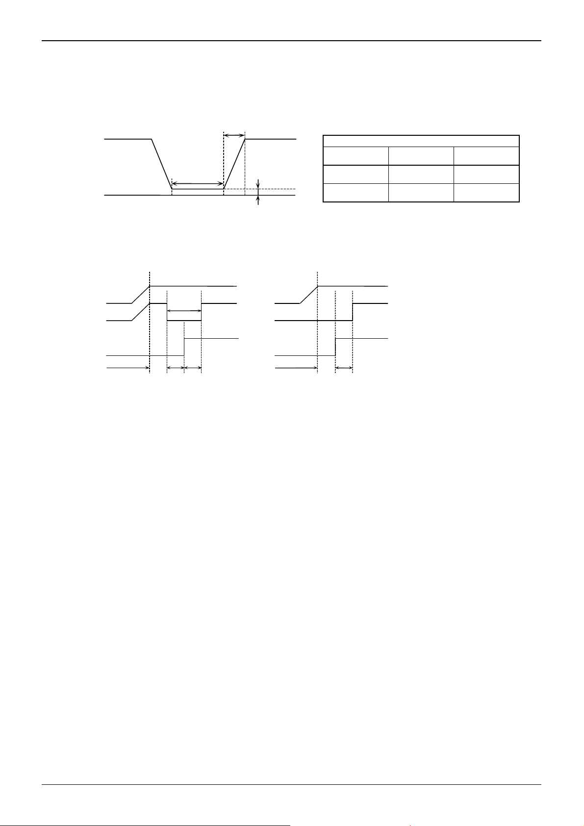
●Notes For Power Supply
CC rises through the low voltage region in which the internal circuit of the IC and the controller are unstable. Therefore,
V
the device may not work properly due to an incomplete reset of the internal circuit. To prevent this, the device has a P.O.R.
CC feature. At power up, maintain the following conditions to ensure functions of P.O.R and LVCC.
and LV
1. "SDA='H'" and "SCL='L' or 'H'".
2. Follow the recommended conditions of t
V
CC
R, tOFF, Vbot for the P.O.R. function during power up.
tR
Recommended conditions of tR, tOFF, Vbot
tR
tOFF
Vbot
tOFF
0
Vbot
Below 10ms
Below 100ms
Above 10ms
Above 10ms
Below 0.3V
Below 0.2V
Fig.33 Vcc rising wave from
3. Prevent SDA and SCL from being "Hi-Z".
In case conditions 1 and/or 2 cannot be met, take following actions:
A)If unable to keep condition 1 ( SDA is "Low" during power up):
→Control SDA ,SCL to be "High" as shown in figure below.
VCC
SCL
SD
fter Vcc becoms stable
Fig.34 SCL="H" and SDA="L"
tLOW
fter Vcc becoms stable
tSU:DAT tDH
Fig.35 SCL="L" and SDA="L"
tSU:DAT
B)If unable to keep condition 2.
→After power becomes stable, execute software reset. (See Fig.29)
C)If unable to keep both conditions 1 and 2.
→Follow the instruction A first, then the instruction B.
●LVCC Circuit
LV
CC circuit inhibits write operation at low voltage, and prevents an inadvertent write. Write operation is inhibited below the
LV
CC voltage (Typ.=1.2V).
●Vcc NOISE
○Bypass Condenser
Noise and surges on power line may cause abnormal function. It is recommended that the bypass condensers (0.1µF) are
attached on the Vcc and GND line beside the device. It is also recommended to attach bypass condensers on the board
close to the connector.
www.rohm.com
19/22
© 2011 ROHM Co., Ltd. All rights reserved.
2011.08 - Rev.C
Page 20

BR24C21,BR24C21F,BR24C21FJ,BR24C21FV,
BU9882-W,BU9882F-W,BU9882FV-W
●Notes for Use
1) Described numeric values and data are design representative values, and the values are not guaranteed.
2) We believe that application circuit examples are recommendable, however, in actual use, confirm characteristics further
sufficiently. In the case of use by changing the fixed number of external parts, make your decision with sufficient margin
in consideration of static characteristics and transition characteristics and fluctuations of external parts and our LSI.
3) Absolute maximum ratings
If the absolute maximum ratings such as impressed voltage and operating temperature range and so forth are
exceeded, LSI may be destructed. Do not impress voltage and temperature exceeding the absolute maximum ratings.
In the case of fear exceeding the absolute maximum ratings, take physical safety countermeasures such as fuses, and
see to it that conditions exceeding the absolute maximum ratings should not be impressed to LSI.
4) GND electric potential
Set the voltage of GND terminal lowest at any action condition. Make sure that each terminal voltages is lower than that
of GND terminal.
5) Heat design
In consideration of permissible dissipation in actual use condition, carry out heat design with sufficient margin.
6) Terminal to terminal shortcircuit and wrong packaging
When to package LSI onto a board, pay sufficient attention to LSI direction and displacement. Wrong packaging may
destruct LSI. And in the case of shortcircuit between LSI terminals and terminals and power source, terminal and GND
owing to foreign matter, LSI may be destructed.
7) Use in a strong electromagnetic field may cause malfunction, therefore, evaluated design sufficiently
Technical Note
www.rohm.com
20/22
© 2011 ROHM Co., Ltd. All rights reserved.
2011.08 - Rev.C
Page 21
BR24C21,BR24C21F,BR24C21FJ,BR24C21FV,
BU9882-W,BU9882F-W,BU9882FV-W
Technical Note
●Ordering part number
B R 2 4 C 2 1 F - E 2
ROHM type BUS type Product type Capacity Package Packaging and forming specification
SOP8
6.2±0.3
SOP-J8
6.0±0.3
0.545
1.375±0.1
SSOP-B8
.
24:I2C 21= 1K
5.0±0.2
(MAX 5.35 include BURR)
7
4.4±0.2
0.595
1.5±0.1
0.11
1.27
4.9±0.2
(MAX 5.25 include BURR)
3.9±0.2
234
1
1.27
0.175
3.0± 0.2
(MAX 3.35 include BURR)
5678
6.4± 0.3
4.4± 0.2
1234
1.15± 0.1
0.1
(0.52)
0.65
6
438251
0.42±0.1
5678
0.1
0.42±0.1
S
S
0.1
0.22
S
S
+0.06
-
4
4°
0.15± 0.1
0.04
+
6
°
−4°
0.17
+
6°
−4°
0.2±0.1
°
+0.1
-
0.05
0.08
0.3MIN
0.9±0.15
(Unit : mm)
0.45MIN
(Unit : mm)
0.3MIN
M
(Unit : mm)
F : SOP8 E2: Embossed tape and reel
FJ : SOP-J8
FV : SSOP-B8
<Tape and Reel information>
Embossed carrier tapeTape
Quantity
Direction
of feed
2500pcs
E2
The direction is the 1pin of product is at the upper left when you hold
()
reel on the left hand and you pull out the tape on the right hand
Reel
<Tape and Reel information>
Embossed carrier tapeTape
Quantity
Direction
of feed
2500pcs
E2
The direction is the 1pin of product is at the upper left when you hold
()
reel on the left hand and you pull out the tape on the right hand
Reel
<Tape and Reel information>
Embossed carrier tapeTape
Quantity
Direction
of feed
2500pcs
E2
The direction is the 1pin of product is at the upper left when you hold
()
reel on the left hand and you pull out the tape on the right hand
Reel
1pin
Order quantity needs to be multiple of the minimum quantity.
∗
1pin
Order quantity needs to be multiple of the minimum quantity.
∗
1pin
Order quantity needs to be multiple of the minimum quantity.
∗
Direction of feed
Direction of feed
Direction of feed
www.rohm.com
21/22
© 2011 ROHM Co., Ltd. All rights reserved.
2011.08 - Rev.C
Page 22
BR24C21,BR24C21F,BR24C21FJ,BR24C21FV,
p
BU9882-W,BU9882F-W,BU9882FV-W
B U 9 8 8 2 F V - W E 2
Technical Note
ROHM type Part No.
Package
SOP14
8.7± 0.2
(MAX 9.05 include BURR)
14
8
<Tape and Reel information>
Quantity
Direction
of feed
6.2± 0.3
4.4± 0.2
1
1.5± 0.1
1.27
0.11
0.4± 0.1
7
0.1
0.3MIN
0.15± 0.1
(Unit : mm)
SSOP-B14
<Tape and Reel information>
Quantity
Direction
of feed
6.4 ± 0.3
0.2
±
4.4
14
1
5.0 ± 0.2
8
0.3Min.
7
0.15 ± 0.1
W: Double cell
F : SOP14
FV : SSOP-B14
Embossed carrier tapeTape
2500pcs
E2
The direction is the 1pin of product is at the upper left when you hold
()
reel on the left hand and you pull out the tape on the right hand
Reel
Embossed carrier tapeTape
2500pcs
E2
The direction is the 1pin of product is at the upper left when you hold
()
reel on the left hand and you pull out the tape on the right hand
Packaging and forming specification
E2: Embossed ta
1pin
Order quantity needs to be multiple of the minimum quantity.
∗
e and reel
Direction of feed
1.15 ± 0.1
0.10
0.65
0.22 ± 0.1
0.1
Direction of feed
(Unit : mm)
Reel
1pin
Order quantity needs to be multiple of the minimum quantity.
∗
www.rohm.com
22/22
© 2011 ROHM Co., Ltd. All rights reserved.
2011.08 - Rev.C
Page 23

Notes
No copying or reproduction of this document, in part or in whole, is permitted without the
consent of ROHM Co.,Ltd.
The content specied herein is subject to change for improvement without notice.
The content specied herein is for the purpose of introducing ROHM's products (hereinafter
"Products"). If you wish to use any such Product, please be sure to refer to the specications,
which can be obtained from ROHM upon request.
Examples of application circuits, circuit constants and any other information contained herein
illustrate the standard usage and operations of the Products. The peripheral conditions must
be taken into account when designing circuits for mass production.
Great care was taken in ensuring the accuracy of the information specied in this document.
However, should you incur any damage arising from any inaccuracy or misprint of such
information, ROHM shall bear no responsibility for such damage.
The technical information specied herein is intended only to show the typical functions of and
examples of application circuits for the Products. ROHM does not grant you, explicitly or
implicitly, any license to use or exercise intellectual property or other rights held by ROHM and
other parties. ROHM shall bear no responsibility whatsoever for any dispute arising from the
use of such technical information.
The Products specied in this document are intended to be used with general-use electronic
equipment or devices (such as audio visual equipment, of ce-automation equipment, communication devices, electronic appliances and amusement devices).
The Products specied in this document are not designed to be radiation tolerant.
While ROHM always makes effor ts to enhance the quality and reliability of its Products, a
Product may fail or malfunction for a variety of reasons.
Please be sure to implement in your equipment using the Products safety measures to guard
against the possibility of physical injury, re or any other damage caused in the event of the
failure of any Product, such as derating, redundancy, re control and fail-safe designs. ROHM
shall bear no responsibility whatsoever for your use of any Product outside of the prescribed
scope or not in accordance with the instruction manual.
The Products are not designed or manufactured to be used with any equipment, device or
system which requires an extremely high level of reliability the failure or malfunction of which
may result in a direct threat to human life or create a risk of human injury (such as a medical
instrument, transportation equipment, aerospace machinery, nuclear-reactor controller, fuelcontroller or other safety device). ROHM shall bear no responsibility in any way for use of any
of the Products for the above special purposes. If a Product is intended to be used for any
such special purpose, please contact a ROHM sales representative before purchasing.
If you intend to export or ship overseas any Product or technology specied herein that may
be controlled under the Foreign Exchange and the Foreign Trade Law, you will be required to
obtain a license or permit under the Law.
Notice
www.rohm.com
© 2011 ROHM Co., Ltd. All rights reserved.
Thank you for your accessing to ROHM product informations.
More detail product informations and catalogs are available, please contact us.
ROHM Customer Support System
http://www.rohm.com/contact/
R1120
A
 Loading...