

Page 1

TECHNICAL NOTE
High-performance Clock Generator Series
3ch Clock Generators
for Digital Cameras
BU2394KN, BU2396KN
●Description
These PLL, single chip ICs generate three types of clocks - CCD, USB, and VIDEO clocks, utilized in digital still and digital
video camera systems. These IC incorporate compact packaging, a simplification of the clock s ystem, and a reduction in
the number of components used for mobile camera equipment.
●Features
1) Connecting a crystal oscillator generates multiple clock signals with a built-in PLL.
2) The CCD clock provides switching selection outputs.
3) Providing the output of low period-jitter clock.
4) Incorporating compact package VQFN-20 most suited for mobile devices.
5) Single power supply of 3.3 V
●Applications
Digital still camera and digital video camera systems
●Product lineup
Parameter BU2394KN BU2396KN
Supply voltage 3.0V~3.6V 3.0V~3.6V
Operating temperature range -5~+70℃ -5~+70℃
14.318182MHz 12.000000MHz Reference input clock
28.636363MHz -
Output CCD clock
Output USB clock 48.008022MHz 12.000000MHz
●Absolute maximum ratings(Ta=25℃)
Parameter Symbol Limit Unit
Supply voltage VDD -0.5~7.0 V
Input voltage VIN -0.5~VDD+0.5 V
Storage Temperature range Tstg -30~125 ℃
Power dissipation PD 530 mW
*1 Operation is not guaranteed.
*2 Reduce by 5.3mW/°C over 25°C
*3 This IC is not designed to be radiation-resistant.
*4 Power dissipation is measured when the IC is mounted to the printed circuit board.
135.000000MHz 36.000000MHz
110.000000MHz 30.000000MHz
108.000000MHz 24.000000MHz
98.181818MHz -
14.318182MHz - Output VIDEO clock
17.734450MHz 27.000000MHz
Ver.B Oct.2005
Page 2

●Recommended operating range
Parameter Symbol Limit Unit
Supply voltage VDD 3.0~3.6 V
Input H voltage VINH 0.8VDD~VDD V
Input L voltage VINL 0.0~0.2VDD V
Operating temperature Topr -5~+70 ℃
Output load CL 15(max.) pF
● Electrical characteristics
BU2394KN(VDD=3.3V, Ta=25℃, unless otherwise specified.)
XTAL_SEL=H with crystal oscillator at a frequency of 28.636363 MHz, while XTAL_SEL=L at 14.318182 MHz
Parameter Symbol
【Action circuit current】
【Output H voltage】
CLK1
CLK2
REF_CLK
【Output L voltage】
CLK1
CLK2
REF_CLK
【Pull-Up resistance value】
FS1, FS2, FS3,
CLK2ON, XTAL_SEL
【Output frequency】
CLK1 FS2:H FS3:H
CLK1 FS2:H FS3:L
CLK1 FS2:L FS3:L
CLK1 FS2:L FS3:H
CLK2
REF_CLK FS1:H
REF_CLK FS1:L
【Output waveform】
Duty1 100MHz or
less
Duty2 100MHz or
more
Rise time
Fall time
【Jitter】
Period-Jitter 1σ
Period-Jitter MIN-MAX P-J
【Output Lock-Time】
Note: The output frequency is determined by the arithmetic (frequency division) expression of a frequency input to XTALIN.
*1 If the input frequency is set to values shown below, the output frequency will be as listed above.
*2 When XTAL_SEL is set to H, the input frequency on XTALIN will be 28.636363 MHz.
*3 When XTAL_SEL is set to L, the input frequency on XTALIN will be 14.318182 MHz.
IDD - 45 60 mA
VOH1 VDD-0.5 VDD-0.2 - V
VOH2 VDD-0.5 VDD-0.2 - V
VOHR VDD-0.5 VDD-0.2 - V
VOL1 - 0.2 0.5 V
VOL2 - 0.2 0.5 V
VOLR - 0.2 0.5 V
Pull-Up
R
Fclk1-1 - 135.000000 - MHz
Fclk1-2 - 108.000000 - MHz
Fclk1-3 - 98.181818 - MHz
Fclk1-4 - 110.000000 - MHz
Fclk2-2 - 48.008022 - MHz
Fref1-1 - 14.318182 - MHz
Fref1-2 - 17.734450 - MHz
Duty1 45 50 55 %
Duty2 - 50 - %
Tr - 2.5 - nsec
Tf - 2.5 - nsec
P-J1σ - 30 - psec
MIN-MAX
Tlock - - 1 msec
Min. Typ. Max.
125 250 375 Ω
- 180 - psec
Limit
2/16
Unit Condition
At no load
When current load = - 9.0mA
When current load = - 7.0mA
When current load = - 4.5mA
When current load =11mA
When current load =9.0mA
When current load =5.5mA
Specified by a current value
running when a voltage of 0V
is applied to a measuring pin.
(R=VDD/I)
XTAL×(1188/63)/2
XTAL×(1056/70)/2
XTAL×(864/63)/2
XTAL×(968/63)/2
XTAL×(228/17)/4
XTAL Output
XTAL×(706/57)/10
Measured at a voltage of 1/2
of VDD
Measured at a voltage of 1/2
of VDD
Period of transition time
required for the output to
reach 80% from 20% of VDD.
Period of transition time
required for the output to
reach 20% from 80% of VDD.
*1
*2
*3
Page 3

BU2396N(VDD=3.3V, Ta=25℃, Crystal =12.000000MHz, unless otherwise specified.)
Parameter Symbol
Limit
Unit Condition
Min. Typ. Max.
【Action circuit current】
IDD - 23 35 mA
At no load
【Output H voltage】
TGCLK
VCLK
UCLK
VOHT VDD-0.5 - - V
VOHV VDD-0.5 - - V
VOHU VDD-0.5 - - V
When current load =-5.0mA
When current load =-5.0mA
When current load =-5.0mA
【Output L voltage】
TGCLK
VCLK
UCLK
VOLT - - 0.5 V
VOLV - - 0.5 V
VOLU - - 0.5 V
When current load =5.0mA
When current load =5.0mA
When current load =5.0mA
【Pull-Up resistance value】
TGCLK_SEL1
TGCLK_SEL2 Pull-up
R
125 250 375 KΩ
Specified by a current value
running when a voltage of 0V is
applied to a measuring pin.
(R=VDD/I)
【Pull-Down resistance value】
TGCLK_EN、TGCLK_PD
VCLK_EN、VCLK_PD Pull-down
R
25 50 75 KΩ
Specified by a current value
running when a VDD is applied to
a measuring pin.
(R=VDD/I)
【Output frequency】
TGCLK SEL1:L SEL2:L
TGCLK SEL1:L SEL2:H
TGCLK SEL1:H
VCLK
UCLK
TGCLK1 - 24.000000 - MHz
TGCLK2 - 30.000000 - MHz
TGCLK3 - 36.000000 - MHz
VCLK - 27.000000 - MHz
UCLK - 12.000000 - MHz
XTAL×(48/4)/6
XTAL×(60/4)/6
XTAL×(54/3)/6
XTAL×(54/3)/8
XTAL output
【Output waveform】
Duty
Rise time
Duty 45 50 55 %
Tr - 2.0 - nsec
Measured at a voltage of 1/2 of VDD
Period of transition time required
for the output to reach 80% from
20% of VDD.
Fall time
Tf - 2.0 - nsec
Period of transition time required
for the output to reach 20% from
80% of VDD.
【Jitter】
Period-Jitter 1σ
P-J1σ - 50 - psec
Period-Jitter MIN-MAX P-J
MIN-MAX
【Output Lock-Time】
Tlock - - 1 msec
- 300 - psec
※1
※2
※3
Note: The output frequency is determined by the arithmetic (frequency division) expression of a frequency input to XTALIN.
If the input frequency is set to 12.000000MHz, the output frequency will be as listed above.
Common to BU2394KN, BU2396KN
※1 Period-Jitter 1σ
This parameter represents standard deviation (=1σ) on cycle distribution data when the output clock c ycles are sampled 1000
times consecutively, with the TDS7104 Digital Phosphor Oscilloscope of Tektronix Japan, Ltd.
※2 Period-Jitter MIN-MAX
This parameter represents a maximum distribution width on cycle distribution data when the output clock cycles are sampled
1000 times consecutively, with the TDS7104 Digital Phosphor Oscilloscope of Tektronix Japan, Ltd.
※3 Output Lock-Time
This parameter represents the elapsed time to reach a voltage of 3.0 V after power supply turns ON and after the system is
switched from power-down to normal operation state, or after the output frequency is switched and is stabilized.
3/16
Page 4

●Reference data (BU2394KN basic data)
1.0V/div
1.0nsec/div
Fig.1 135MHz output wave
At VDD=3.3V and CL=15pF
1.0V/div
500psec/div
Fig.2 135MHz Period-Jitter
At VDD=3.3V and CL=15pF
RBW=1KHz
VBW=100Hz
10dB/div
Fig.3 135MHz Spectrum
At VDD=3.3V and CL=15pF
RBW=1KHz
VBW=100Hz
10KHz/div
1.0V/div
2.0nsec/div
Fig.4 110MHz output wave
At VDD=3.3V and CL=15pF
1.0V/div
2.0nsec/div
Fig.7 108MHz output wave
At VDD=3.3V and CL=15pF
1.0V/div
500psec/div
Fig.5 110MHz Period-Jitter
At VDD=3.3V and CL=15pF
1.0V/div
500psec/div
Fig.8 108MHz Period-Jitter
At VDD=3.3V and CL=15pF
10dB/div
10KHz/div
Fig.6 110MHz Spectrum
At VDD=3.3V and CL=15pF
RBW=1KHz
VBW=100Hz
10dB/div
Fig.9 108MHz Spectrum
At VDD=3.3V and CL=15pF
RBW=1KHz
VBW=100Hz
10KHz/div
1.0V/div
2.0nsec/div
Fig.10 98MHz output wave
At VDD=3.3V and CL=15pF
1.0V/div
500psec/div
Fig.11 98MHz Period-Jitter
At VDD=3.3V and CL=15pF
4/16
10dB/div
10KHz/div
Fig.12 98MHz Spectrum
At VDD=3.3V and CL=15pF
Page 5

●Reference data (BU2394KN basic data)
1.0V/div
5.0nsec/div
Fig.13 48MHz output wave
At VDD=3.3V and CL=15pF
1.0V/div
10.0nsec/div
Fig.16 17.7MHz output wave
At VDD=3.3V and CL=15pF
1.0V/div
10.0nsec/div
Fig.19 14.3MHz output wave
At VDD=3.3V and CL=15pF
1.0V/div
500psec/div
Fig.14 48MHz Period-Jitter
At VDD=3.3V and CL=15pF
1.0V/div
500psec/div
Fig.17 17.7MHz Period-Jitter
At VDD=3.3V and CL=15pF
1.0V/div
500psec/div
Fig.20 14.3MHz Period-Jitter
At VDD=3.3V and CL=15pF
RBW=1KHz
VBW=100Hz
10dB/div
Fig.15 48MHz Spectrum
At VDD=3.3V and CL=15pF
RBW=1KHz
VBW=100Hz
10dB/div
Fig.18 17.7MHz Spectrum
At VDD=3.3V and CL=15pF
RBW=1KHz
VBW=100Hz
10dB/div
Fig.21 14.3MHz Spectrum
At VDD=3.3V and CL=15pF
10KHz/div
10KHz/div
10KHz/div
5/16
Page 6

●Reference data (BU2394KN Temperature and Supply voltage variations data)
55
54
53
52
51
50
Duty[%]
:
49
Duty
48
47
46
45
-25 0 25 50 75 100
Temperature:T[℃]
Fig.22 135MHz
Temperature-Duty
VDD=2.9V
VDD=3.3V
VDD=3.7V
100
90
80
[psec]
70
σ
60
PJ-1
:
50
σ
40
30
20
Period-jitter1
10
0
-25 0 25 50 75 100
Temperature:T[℃]
VDD=2.9V
VDD=3.3V
VDD=3.7V
Fig.23 135MHz
Temperature-Period-Jitter 1σ
55
54
53
52
51
50
Duty[%]
:
49
Duty
48
47
46
45
-25 0 25 50 75 100
Temperature:T[℃]
Fig.25 110MHz
Temperature-Duty
VDD=2.9V
VDD=3.3V
VDD=3.7V
100
90
80
[psec]
70
σ
60
PJ-1
:
50
σ
40
30
20
Period-jitter1
10
0
-25 0 25 50 75 100
Temperature:T[℃]
VDD=2.9V
VDD=3.3V
VDD=3.7V
Fig.26 110MHz
Temperature-Period-Jitter 1σ
55
54
53
52
51
50
Duty[%]
:
49
Duty
48
47
46
45
-25 0 25 50 75 100
Temperature:T[℃]
Fig.28 108MHz
Temperature-Duty
VDD=2.9V
VDD=3.3V
VDD=3.7V
100
90
80
[psec]
70
σ
60
PJ-1
:
50
σ
40
30
20
Period-jitter1
10
0
-25 0 25 50 75 100
Temperature:T[℃]
VDD=2.9V
VDD=3.3V
VDD=3.7V
Fig.29 108MHz
Temperature-Period-Jitter 1σ
55
54
53
52
51
50
Duty[%]
:
49
Duty
48
47
46
45
-25 0 25 50 75 100
Temperature:T[℃]
Fig.31 98MHz
Temperature-Duty
VDD=2.9V
VDD=3.3V
VDD=3.7V
100
90
80
[psec]
70
σ
60
PJ-1
:
50
σ
40
30
20
Period-jitter1
10
0
-25 0 25 50 75 100
Temperature:T[℃]
VDD=2.9V
VDD=3.3V
VDD=3.7V
Fig.32 98MHz
Temperature-Period-Jitter 1σ
6/16
600
500
:
400
300
200
PJ-MIN-MAX[psec]
Period-jitterMIN-MAX
100
0
-25 0 25 50 75 100
Temperature:T[℃]
VDD=2.9V
VDD=3.3V
VDD=3.7V
Fig.24 135MHz
Temperature-Period-Jitter MIN-MAX
600
500
:
400
300
200
PJ-MIN-MAX[psec]
Period-jitterMIN-MAX
100
0
-25 0 25 50 75 100
Temperature:T[℃]
VDD=2.9V
VDD=3.3V
VDD=3.7V
Fig.27 110MHz
Temperature-Period-Jitter MIN-MAX
600
500
:
400
300
200
PJ-MIN-MAX[psec]
Period-jitterMIN-MAX
100
0
-25 0 25 50 75 100
Temperature:T[℃]
VDD=2.9V
VDD=3.3V
VDD=3.7V
Fig.30 108MHz
Temperature-Period-Jitter MIN-MAX
600
500
:
400
300
200
PJ-MIN-MAX[psec]
Period-jitterMIN-MAX
100
0
-25 0 25 50 75 100
Temperature:T[℃]
VDD=2.9V
VDD=3.3V
VDD=3.7V
Fig.33 98MHz
Temperature-Period-Jitter MIN-MAX
Page 7

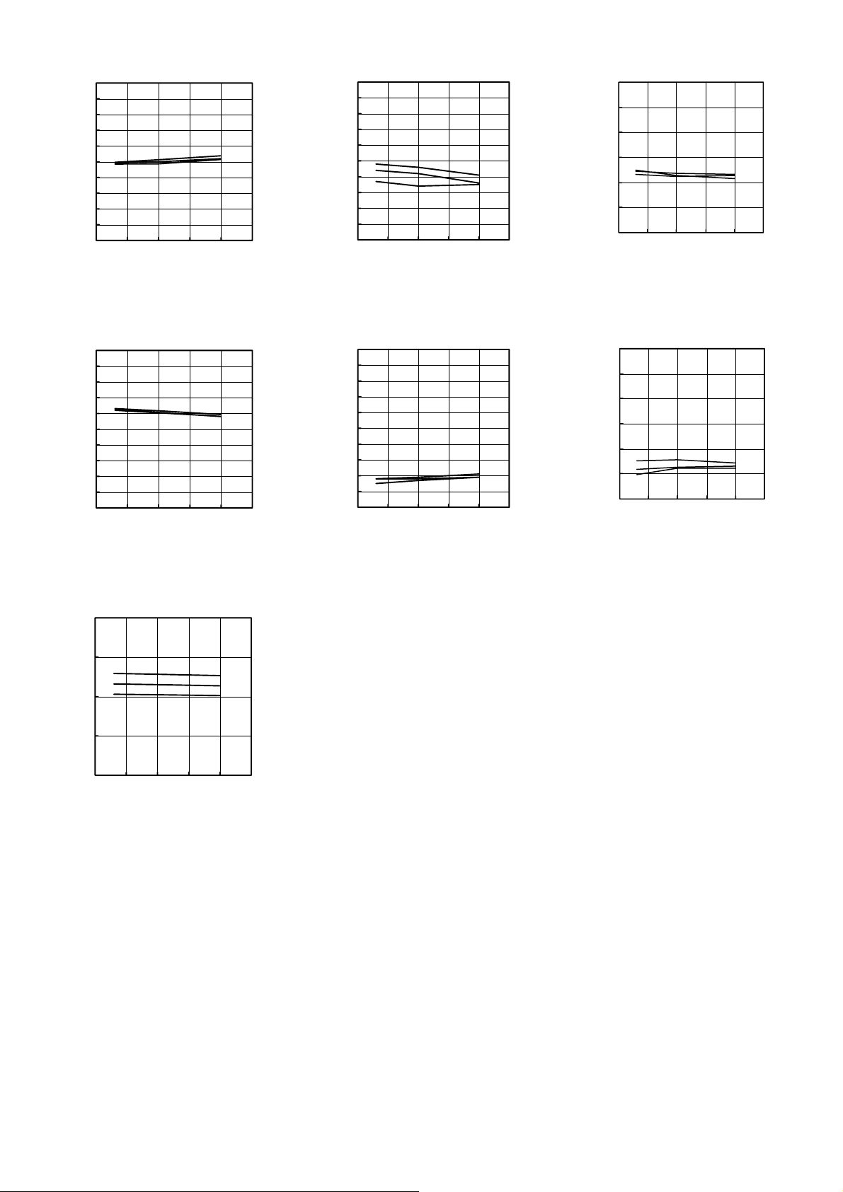
●Reference data (BU2394KN Temperature and Supply voltage variations data)
55
54
53
52
51
50
Duty[%]
:
49
Duty
48
47
46
45
-25 0 25 50 75 100
Temperature:T[℃]
Fig.34 48MHz
Temperature-Duty
VDD=2.9V
VDD=3.3V
VDD=3.7V
100
90
80
[psec]
70
σ
60
PJ-1
:
50
σ
40
30
20
Period-jitter1
10
0
-25 0 25 50 75 100
Temperature:T[℃]
VDD=3.7V
VDD=3.3V
VDD=2.9V
Fig.35 48MHz
Temperature-Period-Jitter 1σ
55
54
53
52
51
50
Duty[%]
:
49
Duty
48
47
46
45
-25 0 25 50 75 100
Temperature:T[℃]
Fig.37 17.7MHz
Temperature-Duty
VDD=2.9V
VDD=3.3V
VDD=3.7V
100
90
80
[psec]
70
σ
60
PJ-1
:
50
σ
40
30
20
Period-jitter1
10
0
-25 0 25 50 75 100
Temperature:T[℃]
VDD=3.7V
VDD=3.3V
VDD=2.9V
Fig.38 17.7MHz
Temperature-Period-Jitter 1σ
55
54
53
52
51
50
Duty[%]
:
49
Duty
48
47
46
45
-25 0 25 50 75 100
Temperature:T[℃]
Fig.40 14.3MHz
Temperature-Duty
VDD=2.9V
VDD=3.3V
VDD=3.7V
100
90
80
[psec]
70
σ
60
PJ-1
:
50
σ
40
30
20
Period-jitter1
10
0
-25 0 25 50 75 100
Temperature:T[℃]
VDD=3.7V
VDD=3.3V
VDD=2.9V
Fig.41 14.3MHz
Temperature-Period-Jitter 1σ
60
50
]
40
30
IDD[mA
:
20
IDD
10
0
-25 0 25 50 75 100
Temperature-Consumption current
Temperature:T[℃]
Fig.43 At 1chip operation
VDD=3.7V
VDD=3.3V
VDD=2.9V
7/16
600
500
:
400
300
200
PJ-MIN-MAX[psec]
Period-jitterMIN-MAX
100
0
-25 0 25 50 75 100
Temperature:T[℃]
VDD=3.7V
VDD=3.3V
VDD=2.9V
Fig.36 98MHz
Temperature-Period-Jitter MIN-MAX
600
500
:
400
300
200
PJ-MIN-MAX[psec]
Period-jitterMIN-MAX
100
0
-25 0 25 50 75 100
Temperature:T[℃]
VDD=3.7V
VDD=3.3V
VDD=2.9V
Fig.39 17.7MHz
Temperature-Period-Jitter MIN-MAX
600
500
:
400
300
200
PJ-MIN-MAX[psec]
Period-jitterMIN-MAX
100
0
-25 0 25 50 75 100
Temperature:T[℃]
VDD=3.7V
VDD=3.3V
VDD=2.9V
Fig.42 14.3MHz
Temperature-Period-Jitter MIN-MAX
Page 8

●Reference data (BU2396KN basic data)
z
1.0V/div
Fig.47 30MHz output waveform
Fig.50 24MHz output waveform
5.0nsec/div
Fig.44 36MHz output waveform
At VDD=3.3V and CL=15pF
1.0V/div
5.0nsec/div
At VDD=3.3V and CL=15pF
1.0V/div
5.0nsec/div
At VDD=3.3V and CL=15pF
1.0V/div
5.0nsec/div
Fig.53 27MHz output waveform
At VDD=3.3V and CL=15pF
1.0V/div
500psec/div
Fig.45 136MHz Period-Jitter
At VDD=3.3V and CL=15pF
1.0V/div
500psec/div
Fig.48 30MHz Period-Jitter
At VDD=3.3V and CL=15pF
1.0V/div
500psec/div
Fig.51 24MHz Period-Jitter
At VDD=3.3V and CL=15pF
1.0V/div
500psec/div
Fig.54 27MHz Period-Jitter
At VDD=3.3V and CL=15pF
8/16
RBW=1KHz
VBW=100Hz
10dB/div
Fig.46 36MHz Spectrum
At VDD=3.3V and CL=15pF
RBW=1KHz
VBW=100Hz
10dB/div
Fig.49 30MHz Spectrum
At VDD=3.3V and CL=15pF
RBW=1KHz
VBW=100Hz
10dB/div
Fig.52 24MHz Spectrum
At VDD=3.3V and CL=15pF
RBW=1KHz
VBW=100Hz
10dB/div
Fig.55 27MHz Spectrum
At VDD=3.3V and CL=15pF
10KHz/div
10KHz/div
10KHz/div
10KHz/div
Page 9

●Reference data (BU2396KN basic data)
1.0V/div
1.0V/div
Fig.56 12MHz output waveform
5.0nsec/div
At VDD=3.3V and CL=15pF
500psec/div
Fig.57 12MHz Period-Jitter
At VDD=3.3V and CL=15pF
●Reference data (BU2396KN Temperature and Supply voltage variations data)
55
54
53
52
51
50
Duty[%]
:
49
Duty
48
47
46
45
-25 0 25 50 75 100
Temperature:T[℃]
Fig.59 36MHz
Temperature-Duty
VDD=2.9V
VDD=3.3V
VDD=3.7V
100
90
80
[psec]
70
σ
60
PJ-1
:
50
σ
40
30
20
Period-jitter1
10
0
-25 0 25 50 75 100
Temperature:T[℃]
VDD=2.9V
VDD=3.3V
VDD=3.7V
Fig.60 36MHz
Temperature-Period-Jitter 1σ
55
54
53
52
51
50
Duty[%]
:
49
Duty
48
47
46
45
-25 0 25 50 75 100
Temperature:T[℃]
Fig.62 30MHz
Temperature-Duty
VDD=2.9V
VDD=3.3V
VDD=3.7V
100
90
80
[psec]
70
σ
60
PJ-1
:
50
σ
40
30
20
Period-jitter1
10
0
-25 0 25 50 75 100
Temperature:T[℃]
VDD=2.9V
VDD=3.3V
VDD=3.7V
Fig.63 30MHz
Temperature-Period-Jitter 1σ
55
54
53
52
51
50
Duty[%]
:
49
Duty
48
47
46
45
-25 0 25 50 75 100
Temperature:T[℃]
Fig.65 24MHz
Temperature-Duty
VDD=2.9V
VDD=3.3V
VDD=3.7V
100
90
80
[psec]
70
σ
60
PJ-1
:
50
σ
40
30
20
Period-jitter1
10
0
-25 0 25 50 75 100
Temperature:T[℃]
VDD=2.9V
VDD=3.3V
VDD=3.7V
Fig.66 24MHz
Temperature-Period-Jitter 1σ
9/16
RBW=1KHz
VBW=100Hz
10dB/div
10KHz/div
Fig.58 12MHz Spectrum
At VDD=3.3V and CL=15pF
600
500
:
400
300
200
PJ-MIN-MAX[psec]
Period-jitterMIN-MAX
100
0
-25 0 25 50 75 100
VDD=2.9V
VDD=3.3V
VDD=3.7V
Temperature:T[℃]
Fig.61 36MHz
Temperature-Period-Jitter MIN-MAX
600
500
:
400
300
200
PJ-MIN-MAX[psec]
Period-jitterMIN-MAX
100
0
-25 0 25 50 75 100
Temperature:T[℃]
VDD=2.9V
VDD=3.3V
VDD=3.7V
Fig.64 30MHz
Temperature-Period-Jitter MIN-MAX
600
500
:
400
300
200
PJ-MIN-MAX[psec]
Period-jitterMIN-MAX
100
0
-25 0 25 50 75 100
Temperature:T[℃]
VDD=2.9V
VDD=3.3V
VDD=3.7V
Fig.67 24MHz
Temperature-Period-Jitter MIN-MAX
Page 10
●Reference data (BU2396KN Temperature and Supply voltage variations data)
55
54
53
52
51
50
Duty[%]
:
49
Duty
48
47
46
45
-25 0 25 50 75 100
Temperature:T[℃]
Fig.68 27MHz
Temperature-Duty
VDD=2.9V
VDD=3.3V
VDD=3.7V
100
90
80
[psec]
70
σ
60
PJ-1
:
50
σ
40
30
20
Period-jitter1
10
0
-25 0 25 50 75 100
Temperature:T[℃]
VDD=3.7V
VDD=3.3V
VDD=2.9V
Fig.69 27MHz
Temperature-Period-Jitter 1σ
55
54
53
52
51
50
Duty[%]
:
49
Duty
48
47
46
45
-25 0 25 50 75 100
Temperature:T[℃]
Fig.71 12MHz
Temperature-Duty
VDD=2.9V
VDD=3.3V
VDD=3.7V
100
90
80
[psec]
70
σ
60
PJ-1
:
50
σ
40
30
20
Period-jitter1
10
0
-25 0 25 50 75 100
Temperature:T[℃]
VDD=2.9V
VDD=3.3V
VDD=3.7V
Fig.72 12MHz
Temperature-Period-Jitter 1σ
40
30
20
:IDD[mA]
IDD
10
VDD=3.7V
VDD=3.3V
VDD=2.9V
0
-25 0 25 50 75 100
Temperature-Consumption current
Temperature:T[℃]
Fig.74 At 1chip operation
10/16
600
500
:
400
300
200
PJ-MIN-MAX[psec]
Period-jitterMIN-MAX
100
0
-25 0 25 50 75 100
Temperature:T[℃]
VDD=3.7V
VDD=3.3V
VDD=2.9V
Fig.70 27MHz
Temperature-Period-Jitter MIN-MAX
600
500
:
400
300
200
PJ-MIN-MAX[psec]
Period-jitterMIN-MAX
100
0
-25 0 25 50 75 100
Temperature:T[℃]
VDD=2.9V
VDD=3.3V
VDD=3.7V
Fig.73 12MHz
Temperature-Period-Jitter MIN-MAX
Page 11

●BU2396KN Operation Modes
When XTAL_SEL=L, (When a crystal oscillator of 14.318182-MHz frequency is used)
Xtal(MHz) CLK2ON FS1 FS2 FS3 CLK1(MHz) CLK2(MHz) REF_CLK(MHz)
14.318182 H H H H 135.000000 48.008022 14.318182
14.318182 H L H H 135.000000 48.008022 17.734450
14.318182 L H H H 135.000000 Fixed to L 14.318182
14.318182 L L H H 135.000000 Fixed to L 17.734450
14.318182 H H H L 108.000000 48.008022 14.318182
14.318182 H L H L 108.000000 48.008022 17.734450
14.318182 L H H L 108.000000 Fixed to L 14.318182
14.318182 L L H L 108.000000 Fixed to L 17.734450
14.318182 H H L L 98.181818 48.008022 14.318182
14.318182 H L L L 98.181818 48.008022 17.734450
14.318182 L H L L 98.181818 Fixed to L 14.318182
14.318182 L L L L 98.181818 Fixed to L 17.734450
14.318182 H H L H 110.000000 48.008022 14.318182
14.318182 H L L H 110.000000 48.008022 17.734450
14.318182 L H L H 110.000000 Fixed to L 14.318182
14.318182 L L L H 110.000000 Fixed to L 17.734450
When XTAL_SEL=H, (When a crystal oscillator of 28.636363MHz frequency is used)
Xtal(MHz) CLK2ON FS1 FS2 FS3 CLK1(MHz) CLK2(MHz) REF_CLK(MHz)
28.636363 H H H H 135.000000 48.008022 14.318182
28.636363 H L H H 135.000000 48.008022 17.734450
28.636363 L H H H 135.000000 Fixed to L 14.318182
28.636363 L L H H 135.000000 Fixed to L 17.734450
28.636363 H H H L 108.000000 48.008022 14.318182
28.636363 H L H L 108.000000 48.008022 17.734450
28.636363 L H H L 108.000000 Fixed to L 14.318182
28.636363 L L H L 108.000000 Fixed to L 17.734450
28.636363 H H L L 98.181818 48.008022 14.318182
28.636363 H L L L 98.181818 48.008022 17.734450
28.636363 L H L L 98.181818 Fixed to L 14.318182
28.636363 L L L L 98.181818 Fixed to L 17.734450
28.636363 H H L H 110.000000 48.008022 14.318182
28.636363 H L L H 110.000000 48.008022 17.734450
28.636363 L H L H 110.000000 Fixed to L 14.318182
28.636363 L L L H 110.000000 Fixed to L 17.734450
1 1 /16
Page 12

●BU2396KN Operation Modes
TGCLK_SEL1 TGCLK_SEL2 TGCLK_EN VCLK_EN TGCLK_PD VCLK_PD
0 0
0 1
1 0
1 1
0 0
0 1
1 0
1 1
0 0
0 1
1 0
1 1
0 0
0 1
1 0
1 1
0 0
0 1
1 0
1 1
0 0 24MHz output
0 1 30MHz output
1 0 36MHz output
1 1
0 0
0 1
1 0
1 1
0 0 24MHz output
0 1 30MHz output
1 0 36MHz output
1 1
0 0
0 1
1 0
1 1
0 0
0 1
1 0
1 1
0 0
0 1
1 0
1 1
0 0
0 1
1 0
1 1
0 0
0 1
1 0
1 1
0 0 24MHz output
0 1 30MHz output
1 0 36MHz output
1 1
0 0
0 1
1 0
1 1
0 0 24MHz output
0 1 30MHz output
1 0 36MHz output
1 1
0
0
1
0 Fixed to L
0
1
1
0
0 Fixed to L
0
1
1
0 Fixed to L
1
1
0
0 Fixed to L
1
0 Fixed to L
0
1
1
1
0 Fixed to L
0
1
1
0 Fixed to L
1
1
TGCLK
Output
36MHz output
36MHz output
36MHz output
output
36MHz
VCLK
Output
Fixed to L
27MHz
output
Fixed to L
27MHz
output
UCLK
Output
12MHz
output
PLL1
30M,24M
Power-Down Power-Down
Normal
operation
Power-Down
Normal
operation
Power-Down
Normal
operation
Power-Down
Normal
operation
Power-Down
Power-Down
Normal
operation
Power-Down
Normal
operation
Power-Down
Normal
operation
Power-Down
Normal
operation
Power-Down
PLL2
36M,27M
Power-Down
Normal
operation
Power-Down
Normal
operation
Power-Down
Normal
operation
Power-Down
Normal
operation
Normal
operation
12/16
Page 13

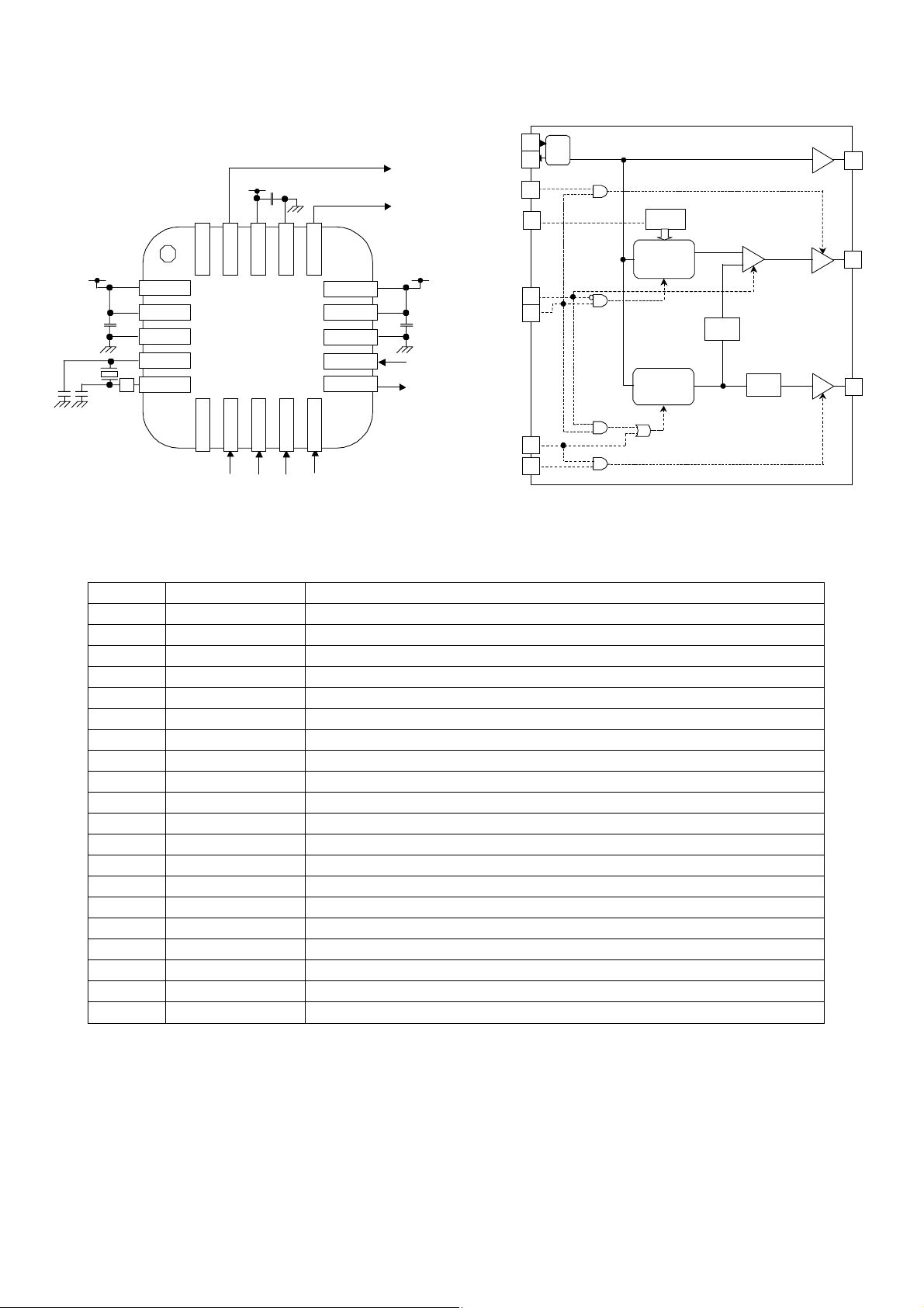
●BU2394KN Application Circuit / Description of Terminal
g
z
z
z
A
z
0.1uF
4:XIN
:TEST2
20
0.1uF
1:AVDD
2:AVDD
3:AVSS
5:XOUT
R
TEST1
:
6
VDD2
:
18
19:REF_CLK
BU2394KN
VQFN-20
FS3
:
8
7:XTAL_SEL
17:VSS2
FS2
:
9
:CLK2OUT
16
FS1
:
10
15:VDD1
14:VDD1
13:VSS1
12
:CLK2ON
11
:CLK1OUT
for Video
14.318182MHz
17.734450MHz
for USB
48.008022MHz
0.1uF
CCD
for
135.000000MH
110.000000MH
108.000000MH
98.181818MHz
XIN
XOUT
XTAL_SEL
CLK2ON
FS1
FS2
FS3
DAT
PLL1
4
XTAL
OSC
5
PLL2
1/2
7
12
10
9
8
PLL3
135.000000MHz
108.000000MHz
110.000000MHz
98.181818MH
48.008022MHz
1/4
17.734450MHz
1/10
14.318182MHz
Fi
.75
Fig.76
Description of Terminal
PIN No. PIN NAME Function
1 AVDD Analog power source
2 AVDD Analog power source
3 AVSS Analog GND
4 XIN Crystal IN
5 XOUT Crystal OUT
6 TEST1 TEST pin, normally open, equipped with pull-down
7 XTAL_SEL Crystal oscillator selection, H: 28.636 MHz, L: 14.318 MHz, equipped with pull-up
8 FS3 CLK1,2 output selection, equi pped with pull-up
9 FS2 CLK1,2 output selection, equi pped with pull-up
10 FS1 REFCLK output selection, equ ipped with pull-up
11 CLK1OUT 110M/98M/108M/135M output
12 CLK2ON CLK2 output control, H: Enable, L: Disable, equipped with pull-up
13 VSS1 CLK1/CLK2 & Internal digital GND
14 VDD1 CLK1/2 & Internal digital power supply
15 VDD1 CLK1/2 & Internal digital power supply
16 CLK2OUT 48M output
17 VSS2 REFCLK GND
18 VDD2 REFCLK power supply
19 REF_CLK 14.3M/17.7M output
20 TEST2 TEST pin, normally open, equipped with pull-down
Note:
• Mount ICs to the printed circuit board for use. (If the ICs are not mounted to the printed circuit board, the characteristics of ICs may not
be fully demonstrated.)
• Mount 0.1µF capacitors in the vicinity of the IC PINs between 1&2 PIN and 3PIN, 13PIN and 14&15PIN, and 17PIN an d 18PIN.
• Although ROHM is confident that the example application circuit reflects the best possible recommendations, be sure to verify circuit
characteristics for your particular application.
• Jitters TYP values vary with the substrate, power supply, output loads, noises, and other. For the use, the operating margin should be
thoroughly checked.
13/16
11
16
19
CLK1
CLK2
REF_CLK
Page 14
●BU2396KN Application Circuit / Description of Terminal
A
z
N
0.1uF
for Video
27.000000MHz
for USB
12.000000MHz
TGCLK_EN
TGCLK_SEL2
VCLK
0.1uF
1:AVDD
2:AVDD
3:AVSS
4:XIN
5:XOUT
R
VCLK_PD
:
20
:
19
BU2396KN
VQFN -20
VDD2
:
18
TEST
:
6
TGCLK_SEL2
TGCLK_SEL1
:
:
7
8
VSS2
:
17
TGCLK_PD
:
9
UCLK
:
16
12:VCLK_EN
TGCLK_E
:
10
15:VDD1
14:VDD1
13:VSS1
11:TGCLK
0.1uF
for
CCD
36.000000MHz
30.000000MHz
24.000000MHz
TGCLK_SEL1
TGCLK_PD
Fig.77
Description of Terminal
PIN No. PIN NAME Function
1 AVDD Analog power source
2 AVDD Analog power source
3 AVSS Analog GND
4 XIN Crystal IN
5 XOUT Crystal OUT
6 TEST TEST pin, normally open, equipped with pull-down
7 TGCLK_SEL2 T G CLK frequency selection, equipped with pull-up
8 TGCLK_SEL1 T G CLK frequency selection, equipped with pull-up
9 TGCLK_PD TGCLK Power-Down control, H: enable, L: Power-Down, equipped with pull-down
10 TGCLK_EN TGCLK output control, H: Enable, L: Output fixed to L, equipped with pull-down
11 TGCLK 36M, 30M, 24M output
12 VCLK_EN VCLK output control, H: enable, L: Output fixed to L, equipped with pull-down
13 VSS1 TGCLK,UCLK & Internal digital GND
14 VDD1 TGCLK,UCLK & Internal digital power supply
15 VDD1 TGCLK,UCLK & Internal digital power supply
16 UCLK 12M output
17 VSS2 VCLK GND
18 VDD2 VCLK power source
19 VCLK 27M output
20 VCLK_PD VCLK Power-Down control, H: enable, L: Power-Down, equipped with pull-down
Note:
• Mount ICs to the printed circuit board for use. (If t he ICs are not mounted to the print ed circuit board, the characteristics of ICs may
not be fully demonstrated.)
• Mount 0.1µF capacitors in the vicinity of the IC PINs between 1&2 PIN and 3PIN, 13PIN and 14&15PIN, and 17PIN and 18PIN.
• Although R OHM is confident that the example application circuit reflects the best possible recommendations, be sure to verify circuit
characteristics for your particular application.
• Jitters TYP values vary with the substrate, power supply, output loads, noises, and other. For the use, the operating margin should be
thoroughly checked.
XIN
XOUT
VCLK_PD
VCL K_EN
4
XTAL
OSC
5
10
7
8
9
20
12
DAT
PLL1
PLL2
12.000000MHz
30.000000MHz
24.000000MH
36.000000MHz
1/6
1/8
27.000000MHz
Fig.78
UCLK
16
11
TGCLK
VCL K
19
14/16
Page 15

●Cautions on Use
1. Absolute Maximum Rat ings
An excess in the absolute maximum ratings, such as supply voltage , temperature range of operating conditions, etc., can
break down devices, thus making impossible to identify breaking mode such as a short circuit or an open circuit. If any
special mode exceeding the absolute maximum ratings is assumed, consider ation should be given to take physical safety
measures including the use of fuses, etc.
2. Recommended operating conditions
These conditions represent a range within which charact eristics can be pr ovided approxi mately as expected. T he electrical
characteristics are guaranteed under the conditions of each parameter.
3. Reverse connection of power supply connector
The reverse connection of power supply connector can break down ICs. Take protective measures against the breakdown
due to the reverse connection, such as mounting an external diode between the po wer supply and the IC’s power supply
terminal.
4. Power supply line
Design PCB pattern to provide low impedance for the wiring between the power supply and the GND lines.
In this regard, for the digital block power supply and the analog block power supply, even though these power supplies has
the same level of potential, separate the power supply pattern for the digital block from that for the analog block, thus
suppressing the diffraction of digital noises to the analog block power supply resulting from impedance common to the wiring
patterns. For the GND line, give consideration to design the patterns in a similar manner.
Furthermore, for all power supply terminals to ICs, mount a capacitor between the power supply and the GND terminal. At
the same time, in order to use an electrolytic capacitor, thoroughly check to be sure the characteristics of the capacitor to be
used present no problem including the occurrence of capacity dropout at a low temperature, thus determining the constant.
5. GND voltage
Make setting of the potential of the GND terminal so that it will be maintained at the minimum in any operating state.
Furthermore, check to be sure no terminals are at a potential lower than the GND voltage including an actual electric
transient.
6. Short circuit between terminals and erroneous mounting
In order to mount ICs on a set PCB, pay thorough attention to the direction and offset of the ICs. Erroneous mounting can
break down the ICs. Furthermore, if a short circuit occurs due to foreign matters entering between terminals or between the
terminal and the power supply or the GND terminal, the ICs can break down.
7. Operation in strong electromagnetic field
Be noted that using ICs in the strong electromagnetic field can malfunction them.
8. Inspection with set PCB
On the inspection with the set PCB, if a capacitor is connected to a low-impedance IC terminal, the IC can suffer stress.
Therefore, be sure to discharge from the set PCB by each process. Furthermore, in order to mount or dismount the set PCB
to/from the jig for the inspection process, be sure to turn OFF the power supply and then mount the set PCB to the jig. After
the completion of the inspection, be sure to turn OFF the power supply and then dismount it from the jig. In addition, for
protection against static electricity, establish a ground for the assembly process and pay thorough attention to the
transportation and the storage of the set PCB.
9. Input terminals
In terms of the construction of IC, parasitic elements are inevitably formed in relation to potential. The operation of the
parasitic element can cause interference with circuit operation, thus resulting in a malfunction and then breakdown of the
input terminal. Therefore, pay thorough attention not to handle the input terminals, such as to apply to the input terminals a
voltage lower than the GND respectively, so that any parasitic element will operate. Furthermore, do not apply a voltage to
the input terminals when no power supply voltage is applied to the IC. In addition, even if the power supply voltage is applied,
apply to the input terminals a voltage lower than the power supply voltage or within the guaranteed value of electrical
characteristics.
10. Ground wiring pattern
If small-signal GND and large-current GND are provided, It will be recommended to separate the large-current GND pattern
from the small-signal GND pattern and establish a single ground at the reference point of the set PCB so that resistance to
the wiring pattern and voltage fluctuations due to a large current will cause no fluctuations in voltages of the small-signal
GND. Pay attention not to cause fluctuations in the GND wiring pattern of external parts as well.
11. External capacitor
In order to use a ceramic capacitor as the external capacitor, determine the constant with consideration given to a
degradation in the nominal capacitance due to DC bias and changes in the capacitance due to temperature, etc.
15/16
Page 16

●Selection of order type
B
U 2 3 9
4
KN
E2
Part No.
Type 23946
Package Type
KN:VQFN
Packing specification
E2: Reel-like emboss taping
B U 2 3 9 K N 2
6
E
Part No. Type 2396 Package Type
KN:VQFN
Packing specification
E2: Reel-like emboss taping
VQFN20
<Dimension>
0.22 ±0.05
(0.6 )
(1.1)
4.2±0.1
4.0±0.1
11
15
16
10
6
20
1
5
0.05
0.22 ± 0.05
+
0.1
−
0.3
4.0±0.1
0.03
+
0.05
0.02
−
0.02
4.2±0.1
(0.5)
0.95MAX
3−(0.35)
(0.22)
0.5
<Tape and Reel information>
Tape
Quantity
Direction
of feed
Embossed carrier tape(with dry pack)
2500pcs
E2
(Correct direction: 1pin of product should be at the upper left when you
hold reel on the left hand, and you pull out the tape on the right hand)
1234
1234
1234
1234
1234
1234
(Unit:mm)
Reel
1pin
Direction of feed
※Orders are available in complete units only.
The contents described herein are correct as of October, 2005
The contents described herein are subject to change without notice. For updates of the latest information, please contact and confirm with ROHM CO.,LTD.
Any part of this application note must not be duplicated or copied without our permission.
Application circuit diagrams and circuit constants contained herein are shown as examples of standard use and operation. Please pay careful attention to the peripheral conditions when designing circuits and deciding
upon circuit constants in the set.
Any data, including, but not limited to application circuit diagrams and information, described herein are intended only as illustrations of such devices and not as the specifications for such devices. ROHM CO.,LTD. disclaims any
warranty that any use of such devices shall be free from infringement of any third party's intellectual property rights or other proprietary rights, and further, assumes no liability of whatsoever nature in the event of any such
infringement, or arising from or connected with or related to the use of such devices.
Upon the sale of any such devices, other than for buyer's right to use such devices itself, resell or otherwise dispose of the same, implied right or license to practice or commercially exploit any intellectual property rights or other
proprietary rights owned or controlled by ROHM CO., LTD. is granted to any such buyer.
The products described herein utilize silicon as the main material.
The products described herein are not designed to be X ray proof.
Published by
Application Engineering Group
Catalog NO.05T421Be '05.10 ROHM C 1000 TSU
Page 17

Appendix
Notes
No technical content pages of this document may be reproduced in any form or transmitted by any
means without prior permission of ROHM CO.,LTD.
The contents described herein are subject to change without notice. The specifications for the
product described in this document are for reference only. Upon actual use, therefore, please request
that specifications to be separately delivered.
Application circuit diagrams and circuit constants contained herein are shown as examples of standard
use and operation. Please pay careful attention to the peripheral conditions when designing circuits
and deciding upon circuit constants in the set.
Any data, including, but not limited to application circuit diagrams information, described herein
are intended only as illustrations of such devices and not as the specifications for such devices. ROHM
CO.,LTD. disclaims any warranty that any use of such devices shall be free from infringement of any
third party's intellectual property rights or other proprietary rights, and further, assumes no liability of
whatsoever nature in the event of any such infringement, or arising from or connected with or related
to the use of such devices.
Upon the sale of any such devices, other than for buyer's right to use such devices itself, resell or
otherwise dispose of the same, no express or implied right or license to practice or commercially
exploit any intellectual property rights or other proprietary rights owned or controlled by
ROHM CO., LTD. is granted to any such buyer.
Products listed in this document are no antiradiation design.
The products listed in this document are designed to be used with ordinary electronic equipment or devices
(such as audio visual equipment, office-automation equipment, communications devices, electrical
appliances and electronic toys).
Should you intend to use these products with equipment or devices which require an extremely high level
of reliability and the malfunction of which would directly endanger human life (such as medical
instruments, transportation equipment, aerospace machinery, nuclear-reactor controllers, fuel controllers
and other safety devices), please be sure to consult with our sales representative in advance.
It is our top priority to supply products with the utmost quality and reliability. However, there is always a chance
of failure due to unexpected factors. Therefore, please take into account the derating characteristics and allow
for sufficient safety features, such as extra margin, anti-flammability, and fail-safe measures when designing in
order to prevent possible accidents that may result in bodily harm or fire caused by component failure. ROHM
cannot be held responsible for any damages arising from the use of the products under conditions out of the
range of the specifications or due to non-compliance with the NOTES specified in this catalog.
Thank you for your accessing to ROHM product informations.
More detail product informations and catalogs are available, please contact your nearest sales office.
ROHM Customer Support System
www.rohm.com
THE AMERICAS / EUROPE / ASIA / JAPAN
Contact us : webmaster@ rohm.co. jp
Copyright © 2008 ROHM CO.,LTD.
21 Saiin Mizosaki-cho, Ukyo-ku, Kyoto 615-8585, Japan
TEL : +81-75-311-2121
FAX : +81-75-315-0172
Appendix1-Rev2.0
 Loading...