

Page 1

1
Multimedia ICs
Clock generator for PD
BU2190F
The BU2190F is a clock generator IC for PD system drives, and uses a single crystal resonator to generate the three
clock signals needed for PD system drives.
•
Applications
PD system
•
Features
1) Clock signals of three different frequencies can be
generated with a single attached crystal resonator.
2) Internal PLL loop filter, eliminating the need for an
attached loop.
3) Single 5.0V power supply.
4) SOP 8-pin package.
•
Block diagram
XTALI
XTALO
16.9344MHz
XTAL
OSC
DATA 2
DATA 1
PLL 1
PLL 2
VREF
1 / 2
1 / 2
BCLK
CLK 1
CLK 2
59.2704MHz
40.2192MHz
16.9344MHz
OE
Page 2

2
Multimedia ICs BU2190F
•
Pin descriptions
Pin No.1Pin name Function Circuit
CLK2 Clock output 2 (f2 = 40.2192MHz)
Ground
Reference oscillation input
Reference oscillation output
Reference oscillation buffer output (fBCLK = 16.9344MHz)
Clock output 1 (f1 = 59.2704MHz)
V
DD
2
B
GND
3
—
XTALI
4
C
XTALO
5
C
BCLK
6
B
CLK1
7
B
V
DD
8
—
OE A
Output enable
OE = H BCLK, CLK1, CLK2, enable
OE = L BCLK, CLK1, disable, CLK2, enable
•
Absolute maximum ratings (Ta = 25°C)
•
Recommended operating conditions (Ta = 25°C)
Parameter Symbol Limits
– 0.5 ~ + 7.0
– 0.5 ~ VDD + 0.5
– 30 ~ + 125
450
Unit
V
V
°C
mW
V
DD
VIN
Tstg
P
D
Applied voltage
Input voltage
Storage temperature
Power dissipation
∗
Does not represent guaranteed performance
∗
Reduced by 4.5mW for increase in Ta of 1°C over 25°C.
䊊 Not designed for radiation resistance.
Parameter Symbol Limits
4.5 ~ 5.5
0.8 × V
DD ~ VDD
0.0 ~ 0.2 × VDD
– 5 ~ + 70
15 (Max.)
Unit
V
V
V
°C
pF
V
DD
VIH
VIL
Topr
CL
Power supply voltage
Input high level voltage
Input low level voltage
Operating temperature
Output load
Page 3
3
Multimedia ICs BU2190F
•
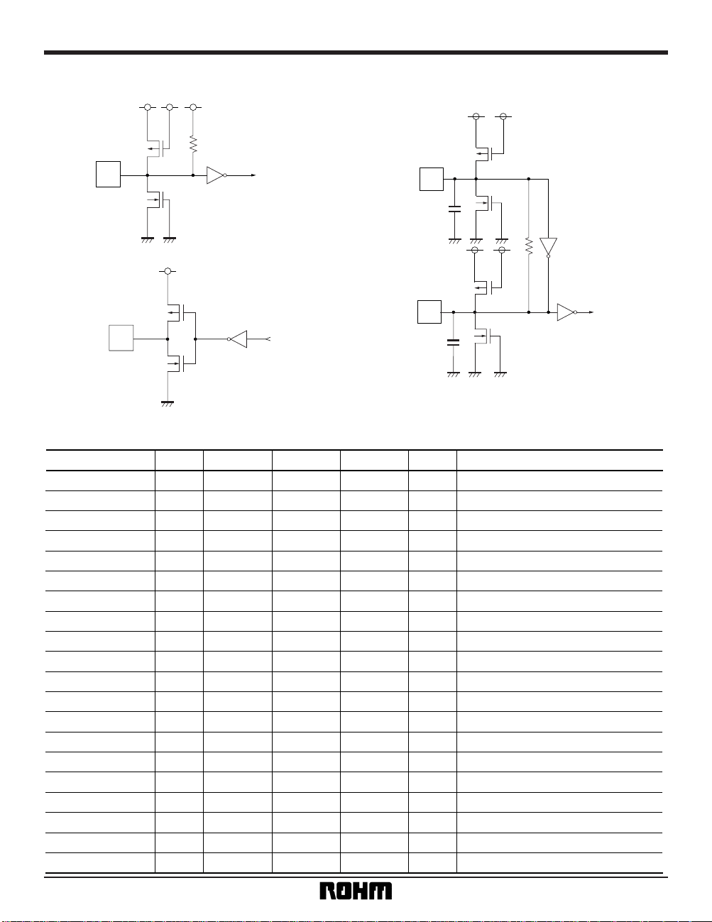
Input / output circuits
Type A
Pin
To inside
Type B
Pin
From inside
Type C
Pin
Pin
To inside
Parameter Symbol Min.
– 125
– 1.0
—
0.7 × V
DD
Typ.
0.0
—
—
Max.
1.0
0.3 × V
DD
—
I
IL
IIH
VIL
VIH
Input low level current
Input high level current
Input low level voltage
Input high level voltage
Unit
µA
µA
V
V
Conditions
V
IN = 5V
V
IN = 0V 5V / 65.5µA = 76KΩ
——0.5VOL
Output low level voltage
VIOL = 4.0mA
0.7 × VDD ——VOH
IDD
Output high level voltage
VIOH = – 4.0mA
—
16.91
16.91
– 100ppm
– 100ppm
16.80
30.00
20.00
40
—
—
—
—
—
30
16.9344
16.9344
59.2704
40.2192
16.9344
59.2704
40.2192
50
50
600
2
10
10
50
16.95
16.95
+ 100ppm
+ 100ppm
17.00
57.2
40.3
60
—
—
—
—
—
f
REF
fBCK
f
1
f2
fBLK1
f1-1
f2-1
DUTY
J1S
Jabs
Tpt
C
IN
COUT
Operating circuit current
Reference frequency (1)
Output frequency (1)
Output frequency (2)
Output frequency (3)
Output frequency (4)
Output frequency (5)
Output frequency (6)
mA
MHz
MHz
MHz
MHz
MHz
MHz
MHz
%
psec
psec
ms
pF
pF
fXTAL = 16.9344MHz, no load
f
REF × 28 / 4 / 2
f
REF × 19 / 4 / 2
V
DD = 3.3V
V
DD = 3.3V
V
DD = 3.3V
Measure at 1 / 2V
DD
Reference value
(1sigma)
Reference value (min.-to-max. width for jitter)
Reference value
Reference value (pin-to-pin capacitance + internal capacitance)
Reference value (pin-to-pin capacitance + internal capacitance)
Duty
Jitter
Jitter
Power up time
XTAL1 equivalent capacitance
XTAL0 equivalent capacitance
– 65.5
– 50.0
•
Electrical characteristics (unless otherwise noted, Ta = 25°C, VDD = 5.0V)
Page 4
4
Multimedia ICs BU2190F
•
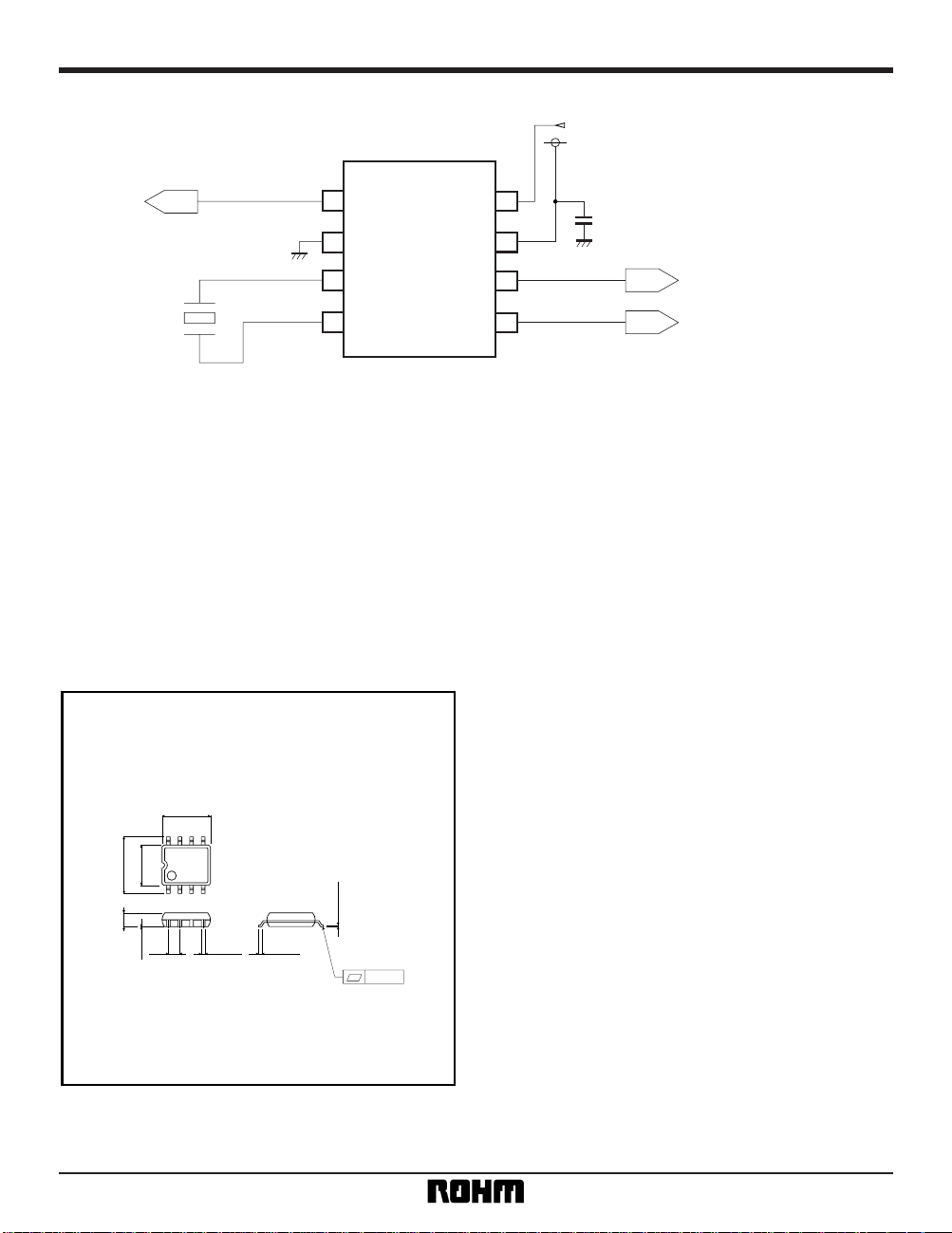
Application example
40.2192MHz
fref = 16.9344MHz
CLK2
GND
XTALI
XTALO
OE
V
DD
CLK1
BCLK
0.1µF
59.2704MHz
16.9344MHz
∗
This IC should be used mounted to a PC board.
If used mounted by a socket, the proper characteristics may not be able to be obtained.
•
Attached components
(1) Crystal oscillator
A crystal resonator with an oscillation frequency of 16.9344MHz is usually sufficient. However, if f
O precision is
necessary, adjust by attaching a capacity to each end of the crystal oscillator.
(2) Power supply
V
DD bypass capacitor
SOP8
0.4 ± 0.11.27
0.15
0.3Min.
0.15 ± 0.1
0.11
6.2 ± 0.3
4.4 ± 0.2
5.0 ± 0.2
85
41
1.5 ± 0.1
•
External dimensions (Units: mm)
 Loading...