

Video Accessory ICs
High Performance VCOs
for Image Sampling
BU2373FV,BU2374FV
●Description
General-purpose VCO Series ICs (BU2373FV and BU2374FV) have a built-in VCO and phase comparator and facilitate the
configuration of a PLL system through the external connection of a LPF and frequency divider.
Furthermore, in order to facilitate the loop constant settings of the PLL system, the application manual has been enhanced to
ensure studies on the application.
●Features
1) The VCO enables midpoint settings within the range of oscillation through the external resistance.
2) The rising edge trigger type of phase comparator is built in.
3) Power-down mode setting can be made independently with the VCO and the phase comparator.
4) The VCO output frequency division can be selected on the SELECT pin.
5) Compact SSOP-B14 Package is adopted.
●Applications
CRT, LCD monitor, and CD-RW
●Line up matrix
BU2373FV BU2374FV
VDD=3.0V ○ -
Supply voltage
VDD=3.3V ○ ○
No.11069EBT07
VDD=5.0V ○ -
VDD=3.0V 37~60MHz -
Frequency
range
VCO-Frequency dividing mode 1/2 1/4
Operating temperature range -20~75℃ -20~75℃
Package SSOP-B14 SSOP-B14
●Absolute maximum ratings (Ta=25℃)
Supply voltage VDD -0.5~7.0 V
Input voltage VIN -0.5~VDD+0.5 V
Storage temperature range Tst g -3 0 ~125 ℃
Power dissipation Pd 400 mW
*1 Operating is not guaranteed.
*2 In the case of exceeding Ta = 25℃, 4.0mW should be reduced per 1℃.
*3 The radiation-resistance design is not carried out.
*4 Power dissipation is measured when the IC is mounted to the printed circuit board.
VDD=3.3V 37~65MHz 37~60MHz
VDD=5.0V 43~100MHz -
Symbol Ratings Unit
www.rohm.com
© 2011 ROHM Co., Ltd. All rights reserved.
1/18
2011.08 - Rev.B
BU2373FV,BU2374FV
●Electrical characteristics
◎BU2373FV(Ta=25℃, VDD=3.0V, unless otherwise specified.)
Parameter Symbol
Min. Typ. Max.
Limits
(VCO)
VCO_IN input impedance Zi - 10 - MΩ
Technical Note
Unit Conditions
Consumption current
(while in normal mode)
Consumption current
(while in standby mode)
Idd(VCO) - 15 - mA With 60 MHz output
Idd_st(VCO) - - 1 µA
VCO_INHIBIT=”H”,
VCOIN=”L”
Control voltage VI 0.5 - VDD-0.5 V
Oscillation range frange 37 - 60 MHz
Bias resistor range Rbias 1.5 - 2.0 KΩ
Frequency sensitivity β1 - 23 - MHz/V
Output duty Duty 45 50 55 %
*1
*2
Measured
at a voltage of 1/2 of VDD
(PFD)
Consumption current
(while in normal mode)
Consumption current
(while in standby mode)
*1 Design guaranteed figures 37 MHz to 45 MHz when Rbias = 2.0 kΩ
50 MHz to 60 MHz when Rbias = 1.5 kΩ
*2 Frequency sensitivity { f1 (VCOIN=2.0V) f2 (VCOIN = 1.0V) } / 1.0V
*3 If the SELECT pin is set to “H” and the output frequency is reduced to 1/2, the frequency range and the frequency sensitivity will be all reduced to 1/2.
Idd(PFD) - 0.5 - mA
Idd_st(PFD) - - 1 µA
When 1 MHz is input to
the FIN_A and B
PFD_INHIBIT=”H”,
FIN_A,B=”L”
BU2373FV(Ta=25℃, VDD=5.0V, unless otherwise specified.)
Parameter Symbol
Min. Typ. Max.
Limits
Unit Conditions
(VCO)
VCO_IN input impedance
Consumption current
(while in normal mode)
Consumption current
(while in standby mode)
Control voltage
Oscillation range
Bias resistor range
Frequency sensitivity
Output duty
Zi - 10 - MΩ
Idd(VCO) - 25 - mA
Idd_st(VCO) - - 1 µA
VI 0.5 - VDD-0.5 V
frange 43 - 100 MHz
Rbias 1.6 - 2.5 KΩ
β1 - 25 - MHz/V
Duty 45 50 55 %
With 60 MHz output
VCO_INHIBIT=”H”,
VCOIN=”L”
*1
*2
Measured
at a voltage of 1/2 of VDD
(PFD)
Consumption current
(while in normal mode)
Consumption current
(while in standby mode)
*1 Design guaranteed figures 43 MHz to 77 MHz when Rbias = 2.5 kΩ
75 MHz to 100 MHz when Rbias = 1.6 kΩ
*2 Frequency sensitivity { f1 (VCOIN = 3.5V) f2 (VCOIN=1.5 V) } / 2.0V
*3 If the SELECT pin is set to “H” and the output frequency is reduced to 1/2, the frequency range and the frequency sensitivity will be all reduced to 1/2.
Idd(PFD) - 1 - mA
Idd_st(PFD) - - 1 µA
When 1 MHz is input to
the FIN_A and B
PFD_INHIBIT=”H”,
FIN_A&B=”L”
www.rohm.com
© 2011 ROHM Co., Ltd. All rights reserved.
2/18
2011.08 - Rev.B
BU2373FV,BU2374FV
◎BU2374FV(Ta=25℃, VDD=3.3V, unless otherwise specified.)
Parameter Symbol
Min. Typ. Max.
Limits
(VCO)
VCO_IN input impedance Zi - 10 - MΩ
Technical Note
Unit Conditions
Consumption current
(while in normal mode)
Consumption current
(while in standby mode)
Idd(VCO) - 12.5 - mA With 50 MHz output
Idd_st(VCO) - - 1 µA
VCO_INHIBIT=”H”,
VCOIN=”L”
Control voltage VI 0.5 - VDD-0.5 V
Oscillation range frange 37 - 60 MHz
Bias resistor range Rbias 2.0 - 3.0 KΩ
Frequency sensitivity β1 - 23 - MHz/V
Output duty Duty 45 50 55 %
*1
*2
Measured at a voltage
of 1/2 of VDD
(PFD)
Consumption current
(while in normal mode)
Consumption current
(while in standby mode)
*1 Design guaranteed figures 37 MHz to 54 MHz when Rbias =2 .0 kΩ
53 MHz to 60 MHz when Rbias = 3.0 kΩ
*2 Frequency sensitivity { f1 (VCOIN = 2.0V) f2 (VCOIN = 1.0 V) } / 1.0V
*3 If the SELECT pin is set to “H” and the output frequency is reduced to 1/4, the frequency range and the frequency sensitivity will be all reduced to 1/4.
Idd(PFD) - 0.5 - mA
Idd_st(PFD) - - 1 µA
When 1 MHz is input to
the FIN_A and B
PFD_INHIBIT=”H”,
FIN_A, B=”L”
www.rohm.com
© 2011 ROHM Co., Ltd. All rights reserved.
3/18
2011.08 - Rev.B
BU2373FV,BU2374FV
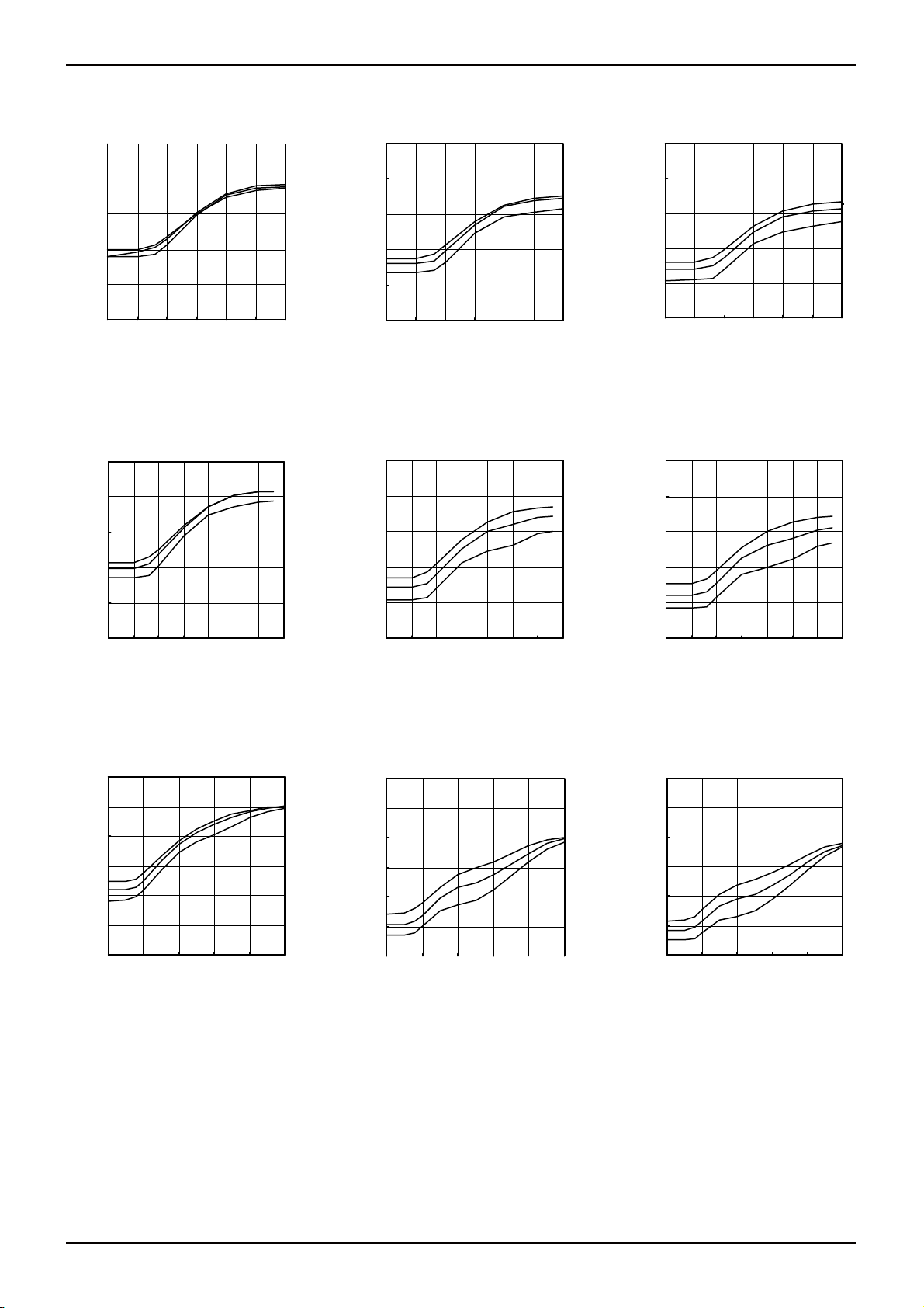
●Reference data
(BU2373FV-Power Voltage Fluctuation Data)
55
54
53
52
51
50
Duty[%]
:
49
Duty
48
47
46
45
-25 0 25 50 75 100
From top:VDD=3.15V
Temper ature:T[℃]
VDD=3.00V
VDD=2.85V
Fig.1 Control Vole Output Frequency
(VDD=3.0V,Rbias=1.5KΩ,Ta=25℃)
100
80
f[MH z]
:
60
40
Output F requency
20
0
0.0 0.5 1.0 1.5 2.0 2.5 3.0 3.5
From top: VDD=3.45V
VDD=3.30V
VDD=3.15V
Contr ol Vol tag e:VI[V]
Fig.4 Control Voltage – Output Frequency
(VDD=3.3V,Rbias=1.6KΩ,Ta=25℃)
150
125
100
f[MH z]
:
75
50
Output F requency
25
0
0.0 1.0 2. 0 3. 0 4. 0 5.0
Fig.7 Control Voltage – Output Frequency
(VDD=5.0V,Rbias=1.6KΩ,Ta=25℃)
From top:VDD=5.25V
VDD=5.00V
VDD=4.75V
Control Voltag e:VI[V]
55
54
53
52
51
50
Duty[%]
:
49
Duty
48
47
46
45
-25 0 25 50 75 100
From top:VDD=3.15V
Temper ature:T[℃]
VDD=3.00V
VDD=2.85V
Fig.2 Control Voltage – Output Frequency
(VDD=3.0V,Rbias=1.8KΩ,Ta=25℃)
100
80
f[MH z]
:
60
40
Output F requency
20
0
0.0 0.5 1.0 1.5 2.0 2.5 3.0 3.5
From top:VDD=3.45V
Control Voltag e:VI[V]
VDD=3.30V
VDD=3.15V
Fig.5 Control Voltage – Output Frequency
(VDD=3.3V,Rbias=2.0 KΩ,Ta=25℃)
150
125
100
f[MH z]
:
75
50
Output F requency
25
0
0.0 1.0 2. 0 3. 0 4. 0 5.0
From top:VDD=5.25V
Contr ol Vol tag e:VI[V]
VDD=5.00V
VDD=4.75V
Fig.8 Control Voltage – Output Frequency
(VDD=5.0V,Rbias=2.4KΩ,Ta=25℃)
Technical Note
100
80
f[MH z]
:
60
40
Output F requency
20
0
0.0 0.5 1.0 1.5 2.0 2.5 3.0 3.5
Fig.3 Control Voltage – Output Frequency
(VDD=3.0V,Rbias=2.0KΩ,Ta=25℃)
100
80
f[MH z]
:
60
40
Output F requency
20
0
0.0 0.5 1.0 1.5 2.0 2.5 3.0 3.5
Fig.6 Control Voltage – Output Frequency
(VDD=3.3V,Rbias=2.2 KΩ,Ta=25℃)
150
125
100
f[MH z]
:
75
50
Output F requency
25
0
0.0 1.0 2. 0 3.0 4. 0 5.0
Fig.9 Control Voltage – Output Frequency
(VDD=5.0V,Rbias=2.7KΩ,Ta=25℃)
From top: VDD=3.15V
VDD=3.00V
VDD=2.85V
Control Voltag e:VI[V]
From top:VDD=3.45V
VDD=3.30V
VDD=3.15V
Contr ol Vol tag e:VI[V]
From top:VDD=5.25V
Control Voltag e:VI[V]
VDD=5.00V
VDD=4.75V
www.rohm.com
© 2011 ROHM Co., Ltd. All rights reserved.
4/18
2011.08 - Rev.B
BU2373FV,BU2374FV
●Reference data
(BU2373FV-Temperature Fluctuation Data)
100
80
f[MH z]
:
60
40
Output F requency
20
0
0.0 0. 5 1.0 1. 5 2.0 2. 5 3.0
Control Voltag e:VI[V]
From top:T=25℃
T=-20℃
T=75℃
Fig.10 Control Voltage – Output Frequency
(VDD=3.0V,Rbias=1.5KΩ)
100
80
f[MH z]
:
60
40
Output F requency
20
0
0.0 0.5 1.0 1.5 2.0 2.5 3.0 3. 5
Fig.13 Control Voltage – Output Frequency
(VDD=3.3V,Rbias=1.6KΩ)
From top:T=75℃
Control Voltag e:VI[V]
T=25℃
T=-20℃
150
125
100
f[MH z]
:
75
50
Output F requency
25
0
0.0 1.0 2. 0 3.0 4.0 5.0
Fig.16 Control Voltage – Output Frequency
(VDD=5.0V,Rbias=1.6KΩ)
From top:T=75℃
T=25℃
T=-20℃
Control Voltag e:VI[V]
100
80
f[MH z]
:
60
40
From top:T=75℃
Output F requency
20
0
0.0 0.5 1.0 1.5 2.0 2.5 3.0
Control Voltage:VI[V]
T=25℃
T=-20℃
Fig.11 Control Voltage – Output Frequency
(VDD=3.0V,Rbias=1.8KΩ)
100
80
f[MH z]
:
60
40
Output F requency
20
0
0.0 0.5 1.0 1.5 2.0 2.5 3.0 3.5
From top:T=75℃
Control Voltage:VI[V]
T=25℃
T=-20℃
Fig.14 Control Voltage – Output Frequency
(VDD=3.3V,Rbias=2.0KΩ)
150
125
100
f[MH z]
:
75
50
Output F requency
25
0
0.0 1.0 2.0 3. 0 4.0 5.0
From top:T=75℃
T=25℃
T=-20℃
Control Voltag e:VI[V]
Fig.17 Control Voltage– Output Frequency
(VDD=5.0V,Rbias=2.4KΩ)
Technical Note
100
80
f[MH z]
:
60
40
From top:T=75℃
Output F requency
20
0
0.0 0.5 1.0 1.5 2.0 2.5 3.0
Control Voltag e:VI[V]
Fig.12 Control Voltage – Output Frequency
(VDD=3.0V,Rbias=2.0 KΩ)
100
80
f[MH z]
:
60
40
Output F requency
20
0
0.0 0.5 1.0 1.5 2.0 2.5 3.0 3.5
Control Voltage:VI[V]
Fig.15 Control Voltage – Output Frequency
(VDD=3.3V,Rbias=2.2KΩ)
150
125
100
f[MH z]
:
75
50
Output F requency
25
0
0.0 1.0 2.0 3. 0 4.0 5.0
Control Voltage:VI[V]
Fig.18 Control Voltage – Output Frequency
(VDD=5.0V,Rbias=2.7KΩ)
T=25℃
T=-20℃
From top:T=75℃
T=25℃
T=-20℃
From top:T=75℃
T=25℃
T=-20℃
www.rohm.com
© 2011 ROHM Co., Ltd. All rights reserved.
5/18
2011.08 - Rev.B

BU2373FV,BU2374FV
●Reference data
(BU2373FV-Recommended Oscillation Range, Frequency - Frequency Sensitivity)
65
Recommended Oscillation Range”H”
60
55
f[MH z]
:
50
45
40
Output F requency
Recommended Oscillation Range”L”
35
30
1.5 1.6 1.7 1. 8 1.9 2.0
Bias Resi stor :Rbi as[K O]
Fig.19 Bias Resistance
- Recommended Oscillation Range
(VDD=3.0V, Select=”L”)
35
Recommended Oscillation Range”H”
30
f[MH z]
:
25
20
Output F requency
Recommended Oscillation Range”L”
15
1.5 1.6 1.7 1.8 1.9 2.0
Bias Resi stor :Rbi as[KO]
Fig.20 Bias Resistance
- Recommended Oscillation Range
(VDD=3.0V, Select=”H”)
70
:
Recommended Oscillation Range”H”
65
60
f[MH z]
55
50
45
40
Output F requency
35
Recommended Oscillation Range”L”
30
1.6 1.7 1. 8 1.9 2.0 2. 1 2.2
Bias Resi stor :Rbi as[KO]
Fig.22 Bias Resistance
- Recommended Oscillation Range
(VDD=3.3V, Select=”L”)
35
Recommended Oscillation Range”H”
30
f[MHz]
:
25
20
Output F requency
Recommended Oscillation Range”L”
15
1.6 1.7 1. 8 1.9 2.0 2.1 2.2
Bias resi stor:R bias[ KO]
Fig.23 Bias Resistance -
Recommended Oscillation Range
(VDD=3.3V, Select=”H”)
110
Recommended Oscillation Range”H”
100
90
f[MH z]
80
:
70
60
50
Output F requency
40
Recommended Oscillation Range”L”
30
1.6 1.8 2. 0 2. 2 2.4 2.6
Bias Resi stor :Rbi as[K O]
Fig.25 Bias Resistance –
Recommended Oscillation Range
(VDD=5.0V, Select=”L”)
55
Recommended Oscillation Range”H”
45
f[MH z]
:
35
25
Output F requency
Recommended Oscillation Range”L”
15
1.6 1.8 2.0 2.2 2.4 2.6
Res istor :Rbi as[KO]
Fig.26 Bias Resistance –
Recommended Oscillation Range
(VDD=5.0V, Select=”H”)
Technical Note
30
25
20
ß1[MH z/v]
:
15
10
5
Fr equency Sensi tivi ty
0
35 40 45 50 55 60
Output F req uency:f[MH z]
Fig.21 Output Frequency
- Frequency Sensitivity
(VDD=3.0V, Select=”L”)
30
25
20
ß1[MH z/v]
:
15
10
5
Fr equency Sensi tivi ty
0
35 40 45 50 55 60 65
Output F req uency:f[MH z]
Fig.24 Output Frequency
- Frequency Sensitivity
(VDD=3.3V, Select=”L”)
30
25
20
ß1[MH z/v]
:
15
10
5
Fr equency Sensi tivi ty
0
40 50 60 70 80 90 10 0
Output F req uency:f[MH z]
Fig.27 Output Frequency
- Frequency Sensitivity
(VDD=5.0V, Select=”L”)
www.rohm.com
© 2011 ROHM Co., Ltd. All rights reserved.
6/18
2011.08 - Rev.B

BU2373FV,BU2374FV
]
●Reference data
(BU2374FV-Power Voltage Fluctuation Data)
100
80
f[MH z]
:
60
100
80
f[MH z]
:
60
40
Output Fr equency
20
0
0.0 0. 5 1.0 1.5 2.0 2.5 3.0 3. 5
From top:VDD=3.45V
Control Voltag e:VI[V]
VDD=3.30V
VDD=3.15V
40
Output F requency
20
0
0.0 0.5 1.0 1.5 2.0 2.5 3.0 3.5
From top:VDD=3.45V
Contr ol Vol tag e:VI[V]
VDD=3.30V
VDD=3.15V
Fig.28 Control Voltage Output Frequency
(VDD=3.3V,Rbias=2.0KΩ,Ta=25℃)
Fig.29 Control Voltage
(VDD=3.3V,Rbias=2.4 KΩ,Ta=25℃)
Output Frequency
●Reference data
(BU2374FV-Temperature Fluctuation Data)
100
80
f[MH z]
:
60
100
80
f[MH z]
:
60
40
Output F requency
20
From top:T=75
0
0.0 0.5 1.0 1. 5 2.0 2.5 3.0 3.5
Fig.31 Control Voltage Output Frequency
Control Voltag e
(VDD=3.3V,Rbias=2.0KΩ)
VI[V]
:
T=25
T=-20
℃
℃
℃
40
Output F requency
20
0
0.0 0.5 1.0 1.5 2.0 2.5 3.0 3.5
Control Voltag e:VI[V]
From top:T=75
T=25
T=-20
℃
℃
℃
Fig.32 Control Voltage Output Frequency
(VDD=3.3V,Rbias=2.4KΩ)
●Reference data
(BU2374FV-Recommended Oscillation Range, Frequency - Frequency Sensitivity)
100
25
80
Recommended Oscillation Range”H”
f[MH z]
:
60
20
Recommended Oscillation Range”H”
f[MH z]
:
15
40
Output F requency
Recommended Oscillation Range”L”
20
10
Recommended Oscillation Range”L”
Output F requency
5
0
2.0 2.2 2.4 2.6 2.8 3.0
– Recommended Oscillation Range
Res istor :Rbi as[KO]
Fig.34 Bias Resistance
(VDD=3.3V, Select=”L”)
0
2.0 2.2 2.4 2.6 2.8 3.0
Res istor :Rbi as[KO]
Fig.35 Bias Resistance
– Recommended Oscillation Range
(VDD=3.3V, Select=”H”)
Technical Note
100
80
f[MH z]
:
60
40
Output F requency
20
0
0.0 0.5 1.0 1. 5 2.0 2.5 3. 0 3.5
Fig.30Control Voltage Output Frequency
(VDD=3.3V,Rbias=3.0KΩ,Ta=25℃)
100
80
f[MH z]
:
60
40
Output F requency
20
0
0.0 0. 5 1.0 1.5 2. 0 2. 5 3.0 3.5
Fig.33 Control Voltage
(VDD=3.3V,Rbias=3.0KΩ)
50
45
40
35
30
25
20
15
10
Fr equency sens itiv ity: ß 1[MH z/v
5
0
35 40 45 50 55 60
Fig.36 Output Frequency
- Frequency Sensitivity
(VDD=3.3V, Select=”L”)
From top:VDD=3.45V
VDD=3.30V
VDD=3.15V
Control Voltag e:VI[V]
From top:T=75
Control Voltage:VI[V]
Output Frequency
Fr equency: f[ MH z]
T=25
T=-20
℃
℃
℃
www.rohm.com
© 2011 ROHM Co., Ltd. All rights reserved.
7/18
2011.08 - Rev.B

BU2373FV,BU2374FV
●Reference data
(BU2373FV-VCO Free-run Output Characteristics)
RBW:30kHz
VBW:30kHz
10dB/div
Fig.37 Spectrum Waveform
(VDD=3.0V,Select=”L”,Output=50MHz)
100kHz/div
RBW:30kHz
VBW:30kHz
10dB/div
Fig40 Spectrum Waveform
(VDD=3.3V,Select=”L”,Output=50MHz)
100kHz/div
RBW:30kHz
VBW:30kHz
10dB/div
Fig.43 Spectrum Waveform
(VDD=5.0V,Select=”L”,Output=75MHz)
100kHz/div
●Reference data
(BU2374FV-VCO Free-run Output Characteristics)
RBW:30kHz
VBW:30kHz
10dB/div
Fig.46 Spectrum Waveform
(VDD=3.3V,Select=”L”,Output=50MHz)
100kHz/div
1V/div
5nsec/div
Fig.38 Output Waveform
(VDD=3.0V,Select=”L”,Output=50MHz)
1V/div
5nsec/div
Fig.41 Output Waveform
(VDD=3.3V, Select=”L”, Output=50MHz)
1V/div
2nsec/div
Fig.44 Output Waveform
(VDD=5.0V,Select=”L”,Output=75MHz)
1V/div
5nsec/div
Fig.47 Output Waveform
(VDD=3.3V,Select=”L”,Output=50MHz)
Technical Note
1V/div
500psec/div
Fig.39 Period-Jitter Waveform
(VDD=3.0V,Select=”L”,Output=50MHz)
1V/div
500psec/div
Fig.42 Period-Jitter Waveform
(VDD=3.3V,Select =”L”, Output=50MHz)
1V/div
500psec/div
Fig.45 Period-Jitter Waveform
(VDD=5.0V,Select=”L”,Output=75MHz)
1V/div
500psec/div
Fig.48 Period-Jitter Waveform
(VDD=3.3V,Select=”L”,Output=50MHz)
www.rohm.com
© 2011 ROHM Co., Ltd. All rights reserved.
8/18
2011.08 - Rev.B

BU2373FV,BU2374FV
A
A
●Block diagram
(BU2373FV)
1:LOGIC_VDD
2:SELECT
3:VCO_OUT
4:FIN_A
5:FIN_B
6:PFD_OUT
7:LOGIC_GND
SSOP-B14
14:VCO_VDD
BU2373FV
13:BIAS
12:VCO_IN
11:VCO_GND
10:VCO_INHIBIT
9:PFD_INHIBIT
8:TEST
(BU2374FV)
1:LOGIC_VDD
2:SELECT
3:VCO_OUT
4:FIN_A
5:FIN_B
6:PFD_OUT
7:LOGIC_GND
SSOP-B14
BU2374FV
14:VCO_VDD
13:BIAS
12:VCO_IN
11:VCO_GND
10:VCO_INHIBIT
9:PFD_INHIBIT
8:TEST
2PIN:SELECT
3PIN:VCO _OU T
4PIN
:FIN_
5PIN:FIN_B
6PIN
:PFD_OUT
2PIN:SELECT
3PIN:VCO_OUT
4PIN
:FIN_
5PIN:FIN_B
6PIN
:PFD_OUT
Pmos Gate
Nmos Gate
Pmos Gate
Nmos Gate
Through
or 1/2
Phase
Detector
Through
or 1/4
Phase
Detector
Level
Shifter
Fig.49
Level
Shifter
Fig.50
VCO
VCO
Technical Note
13PIN
:BIAS
12PIN
:VCO_IN
10PIN
:VCO_INHIBIT
9PIN
:PFD_INHIBIT
13PIN
:BIAS
12PIN
:VCO_IN
10PIN
:VCO_INHIBIT
9PIN
:PFD_INHIBIT
www.rohm.com
© 2011 ROHM Co., Ltd. All rights reserved.
9/18
2011.08 - Rev.B

BU2373FV,BU2374FV
●Pin assignment function
PIN NO. PIN name Function
Technical Note
1 LOGIC_VDD
2 SELECT
Power supply for the internal Logic and the VCO output,
which should be separated from power supply for the VCO_VDD (analog block).
VCO output frequency dividing mode selection pin.
H: Frequency dividing output, L: Through output
3 VCO_OUT VCO output pin. If the VCO_INHIBIT is set to “H”, the VCO_OUT will be fixed to L.
4 FIN-A Reference frequency input pin
5 FIN-B
6 PFD_OUT
VCO block frequency dividing input pin,
which inputs after the VCO output frequency is divided through the external counter.
Phase comparator output pin. If the PFD_INHIBIT is set to “H”,
the PFD_OUT will be set to Hi-Z output.
7 LOGIC_GND GND for the internal Logic and the VCO output
8 TEST
9 PFD_INHIBIT
10 VCO_INHIBIT
Test mode pin, which is normally used with set to OPEN or fixed to L.
Equipped with Pull-down resistor.
Phase comparator inhibit control pin.
If the PFD_INHIBIT is set to “H”, the PFD_OUT will be set to Hi-Z output.
VCO inhibit control pin.
If the VCO_INHIBIT is set to “H”, the VCO_OUT will be fixed to L output.
11 VCO_GND GND for VCO (Analog block GND)
12 VCO_IN
13 BIAS
VCO control pin, to which loop filter output
for the PLL system is connected due to frequency control on normal system.
Bias current setting pin for the shift of VCO oscillation range.
A resistor is connected to the VCO_VDD for the control of bias current.
14 VCO_VDD VDD for VCO (power supply for analog block)
●Example of application circuit
H:VCO_OUT divide
L:VCO_OUT normal
1/N
Divider
Please separate completely the bypass capacitor between an analog power supply and
GND from a digital power supply and GND . Please insert an about 0.01µF bypass
capacitor near the pin as much as possible .
Please adjust so that the voltage of VCO_IN
1
LOGIC_VDD
2
SELECT
3
VCO_OUT
4
FIN_A
5
FIN_B
6
PFD_OUT
LOGIC_GND
7
VCO_VDD
BIAS
VCO_IN
VCO_GND
VCO_INHIBIT
PFD_INHIBIT
TEST
14
13
12
11
10
9
8
is set to 1/2VDD.
R2
R1
C1
C2
H:PFD_OUT disable
L:PFD_OUT enable
recommend a lug lead filter.
H:VCO_OUT disable
L:VCO_OUT enable
The bypass capacitor between a digital power supply and GND should set aside
an analog power supply and GND. Please insert an about 0.01uF bypass
capacitor near the pin as much as possible .
Fig.51
* It is recommended to use bypass capacitors of good high-frequency characteristics.
* It is recommended to apply power supply in the LOGIC_VDD and LOGIC_GND circuits for the SELECT. PFD_INHIBIT, and VCO_INHIBIT control pins.
www.rohm.com
© 2011 ROHM Co., Ltd. All rights reserved.
10/18
2011.08 - Rev.B

BU2373FV,BU2374FV
g
r
Technical Note
●Description of operations
VCO Block
Our VCO block consists of ring oscillators using 5-step reverse Amp. Setting the 2PIN: SELECT to “H” makes it possible to
set the system to output frequency dividing mode. (The frequency is divided to 1/2 on the BU2373FV, while 1/4 on the
BU2374FV.) 50% of the frequency is guaranteed even to the duty at this time.
Furthermore, setting the 10Pin: VCO_INHIBIT to “H” makes it possible to set the system to power-down mode. While in
power-down mode, the VCO_OUT output is fixed to “L”, thus achieving reduction in Analog consumption current
approximately by 80%.
In addition, through the adjustment of external resistance value for the BIAS terminal on 13Pin, the fine adjustment of
output frequency can be made.
(VCO I/O Characteristics)
frequency
(MHz)
It is possible to adjust
center frequency with biasresistor
0
Fig.52
VCO_IN (V)
* The VCO built in the BU2373FV has been designed to provide the lowest frequency sensitivity when using the VCO_IN
at about VDD/2. To make use of the VCO, it is recommended to adjust the BIAS resistance so that the voltage of the
VCO_IN will reach VDD/2.
(Configuration of VCO Block)
VCOIN
Bias
block
Level
Shifte
VCO_INHIBIT
L
1/2 1/2
H
SELECT
VCO_OUT
.53
Fi
www.rohm.com
© 2011 ROHM Co., Ltd. All rights reserved.
11/18
2011.08 - Rev.B

BU2373FV,BU2374FV
Technical Note
Phase Comparator
Our phase comparator is of rising edge detection type. This phase comparator shows the characteristics shown below.
(1) The phase comparator outputs an error pulse (UP signal) after the rising edge is detected at the FIN-A until the
rising edge is detected at the FIN-B, and then it is reset.
(2) The phase comparator outputs an error pulse (DOWN signal) after the rising edge is detected at the FIN-B until the
rising edge is detected at the FIN-A, and then it is reset.
Furthermore, setting the 9Pin: PFD_INHIBIT to “H” makes it possible to set the system to power-down mode. While in
power-down mode, the PFD_OUT outputs high impedance. In other words, it is brought to reset state with the Logic power
supply. (A leak current of 1 A or less is guaranteed.)
(I/O Characteristics of Phase Comparator)
FIN-A
FIN-B
PFD_OUT
Fig.54
●Reference data
(Common to BU2373FV & BU2374FV – Phase Comparator I/O Waveform)
1V/div
1V/div
1V/div
Upper:FIN_A
Middle:FIN_B
Lower:PFD_OUT
(VDD=3.3V, FIN_A > FIN_B)
50µsec/div
Fig.55 UP Signal Output
Upper:FIN_A
Middle:FIN_B
Lower:PFD_OUT
50µsec/div
Fig.56 No Error Signal Output
(VDD=3.3V, FIN_A = FIN_B)
Upper:FIN_A
Middle:FIN_B
Lower:PFD_OUT
50µsec/div
Fig.57 DOWN Signal Output
(VDD=3.3V, FIN_A < FIN_B)
www.rohm.com
© 2011 ROHM Co., Ltd. All rights reserved.
12/18
2011.08 - Rev.B

BU2373FV,BU2374FV
g
x
y
A
Technical Note
(Functioning of PLL System)
In order to configure the stable PLL system, the following section describes the functional principle, open loop
characteristics, and closed loop characteristics by block shown in the Block Diagram below.
PLL System Block Diagram
FIN-
θ
FIN-B
θ
Phase-comparator
i
Kp
o
VCOLPF
F(s) Kv/s
VCO_OUT
1/N
Divider
Fi
.58
① Phase Comparator
The phase comparator shows the characteristics shown in figure below. Assuming that the Gain is Kp,
Kp=(VOHVOL)/4(V/rad)
② VCO (Voltage Controlled Oscillator)
The VCO shows the characteristics shown in figure below.
Assuming that the Gain is Kv, Kv=2 (fmax-fmin)/(Vmax-Vmin)(rad/s/V)
VOH
frequenc
(MHz)
fm a
-2
π
0
2
π
VOL
fm in
0
Vm in
Vm ax
VCO_IN (V)
Fig.59 Phase Comparator Characteristics Fig.60 VCO Characteristics
③ LPF (Lag-Lead Filter)
Calculate the Gain of the lag-lead filter. It is recommended to use the filter having the pattern shown below.
PDOUT VCOIN
R2
R1
C1
C2
Fig.61
www.rohm.com
© 2011 ROHM Co., Ltd. All rights reserved.
13/18
2011.08 - Rev.B

BU2373FV,BU2374FV
Technical Note
For the lag-lead filter afore-mentioned, assuming that C1 C2 (C2 is used at a value approx. 10 times as high as C1),
break this filter into two portions as shown below to facilitate the calculation, thus proceeding with the calculation.
(1) (2)
R2
R2
R1
C2
R1
C1
Fig.62 LPF Portion ① Fig.63 LPF Portion ②
In the case of (1) above,
F(s) =
VOUT
VIN
R1+
=
R1+R2+
| F(jω) | = (ω=2πf)
)
φ(ω
1+{ω・C2・(R1+R2)
-1
=
(ω・C2・R1)-tan-1{ω・C2・(R1+R2) }
tan
1+
2
・C22・R1
ω
2
1
S・C2
1
S・C2
2
}
=(S=j
S・C2・R1+1
S・C2・(R1+R2)+1
ω
)
・By the expression above, the Gain and the Phase are given as shown in graphs below.
Gain(dB)
<Gain>
φ
-6dB/oct
<Phase>
f
C1
f
C2
f
π/4
20log{R1/(R1+R2)}
f
C1
f
C2
f
π/2
Fig.64 (Fig.62) Frequency Gain Characteristics Fig.65 (Fig.62) Frequency Phase Characteristics
f
C1
1
=
×
2
π
1
fc2 =
,
1
×
2
π
1
C2・R1C2・(R1+R2)
In the case of (2) above,
F(s) =
VOUT
VIN
=
R2+
| F(jω) | = (ω=2πf)
1+
ω
2
・C12・
(R1+R2)
R1 R1
1+S・C1・R1
R1
=
1+S・C1・R1
2
R1
2
2
・R2
2
2
R1
(R1+R2)
S・C1・
R1+R2
R1・R2
R1+R2
(S=jω)
+1
φ(ω
)=
-tan
-1
{ω・C1・
R1・R2
(R1+R2)
}
www.rohm.com
© 2011 ROHM Co., Ltd. All rights reserved.
14/18
2011.08 - Rev.B

BU2373FV,BU2374FV
・By the expression aforementioned, the Gain and the Phase are given as shown in graphs below.
Gain(dB)
20log{R1/(R1+R2)}
<Gain>
φ
-6dB/oct
π/4
<Phase>
f
C3
π/2
Fig.66 (Fig.63) Frequency Gain Characteristics Fig.67 (Fig.63) Frequency Phase Characteristics
f
C3
f
f
C3
1
=
2
π
×
C1・R1・R2
R1+R2
By combining (1) and (2), finding the Gain and the Phase of the lag-lead filter,
F(s) =
VOUT
VIN
=
{1+S・C2・(R1+R2)} × {1+ S・C1・
1+S・C2・R1
R1・R2
R1+R2
(S=jω)
}
The gain and the Phase are given as shown below, respectively.
Gain=20・log{
G1=
G2=
1+C2
1+C2
G3=
1+C12・R12・
G2
G1×G3
2
・(R1+R2)2・(2πf)
2
・R12・(2πf)
}
2
1
(R1+R2)
Phase=θ2-θ1-θ3
,
2
,
,
・(2πf)
2
,
2
θ
θ
θ
1=
2=
3=
-1
{2πf・C2・(R1+R2)}
-tan
-1
(2πf・C2・R1)
tan
-1
{2πf・C1・
-tan
R1・R2
(R1+R2)
Gain(dB)
<Gain>
-6dB/oct
φ
f
<Phase>
C1
f
C2
f
π/4
20log{R1/(R1+R2)}
f
f
C1
f
C2
C3
f
π/2
Fig.68 (Fig.61) Frequency
Gain Characteristics Fig.69 (Fig.61) Frequency Phase Characteristics
Technical Note
f
}
C3
f
www.rohm.com
© 2011 ROHM Co., Ltd. All rights reserved.
15/18
2011.08 - Rev.B

BU2373FV,BU2374FV
Technical Note
・Where, find the Gain for the open loop of PLL system. Assuming that the transfer function is H(s),
H(s)=
Kp×F(s)×
Kv
SN
1
×
G0=
PLL-Gain=20・log{
Kv
Kp×
SN
×
2πf×N
Kp×Kv
1
=
2
G1×G3×G0
S×
G2
1
Kp×Kv
,
θ
N
0=
}
-1
(2πf・
-tan
Phase=-θ0+θ2-θ1-θ3
,
N
Kp×Kv 2
)=
π
Gain(dB)
<Gain>
φ
f
C1
<Phas e>
f
C2
f
C3
π/2
f
C1
f
C2
f
C3
f
π
Fig.70 (Fig.58) Frequency Gain Characteristics
Fig.71 (Fig.58) Frequency Phase Characteristics
If, by the expression above, the LPF constant is selected so that a phase margin of 45 or more is secured when the
Gain for the open loop becomes 0 dB, the PLL system will stably function.
Note)
・As to the jitters, the TYP values vary with the substrate, power supply, output loads, noises, and others. Besides, for the
use of the BU2373FV or the BU2374FV, the operating margin should be thoroughly checked.
・The Analog power supply and the Logic power supply should be separated from each other so that noises generated with
the Logic power supply have no adverse influences on the Analog power one.
・Bypass capacitors between the power supply and GND should be mounted as close as possible.
・Power to control pins (i.e., VCO_INHIBIT, PFD_INHIBIT and SELECT) should be supplied from the logic power supply.
・In order to configure the PLL system, the LPF GND should be connected to the Analog GND and mounted in the
proximity of the VCO_IN.
f
www.rohm.com
© 2011 ROHM Co., Ltd. All rights reserved.
16/18
2011.08 - Rev.B

BU2373FV,BU2374FV
●Notes for use
(1) Absolute Maximum Ratings
An excess in the absolute maximum ratings, such as applied voltage (VDD or VIN), operating temperature range (Topr),
etc., can break down devices, thus making impossible to identify breaking mode such as a short circuit or an open circuit.
If any special mode exceeding the absolute maximum ratings is assumed, consideration should be given to take physical
safety measures including the use of fuses, etc.
(2) Recommended operating conditions
These conditions represent a range within which characteristics can be provided approximately as expected. The
electrical characteristics are guaranteed under the conditions of each parameter.
(3) Reverse connection of power supply connector
The reverse connection of power supply connector can break down ICs. Take protective measures against the breakdown
due to the reverse connection, such as mounting an external diode between the power supply and the IC’s power supply
terminal.
(4) Power supply line
Design PCB pattern to provide low impedance for the wiring between the power supply and the GND lines.
In this regard, for the digital block power supply and the analog block power supply, even though these power supplies has
the same level of potential, separate the power supply pattern for the digital block from that for the analog block, thus
suppressing the diffraction of digital noises to the analog block power supply resulting from impedance common to the
wiring patterns. For the GND line, give consideration to design the patterns in a similar manner.
Furthermore, for all power supply terminals to ICs, mount a capacitor between the power supply and the GND terminal. At
the same time, in order to use an electrolytic capacitor, thoroughly check to be sure the characteristics of the capacitor to
be used present no problem including the occurrence of capacity dropout at a low temperature, thus determining the
constant.
(5) GND voltage
Make setting of the potential of the GND terminal so that it will be maintained at the minimum in any operating state.
Furthermore, check to be sure no terminals are at a potential lower than the GND voltage including an actual electric
transient.
(6) Short circuit between terminals and erroneous mounting
In order to mount ICs on a set PCB, pay thorough attention to the direction and offset of the ICs. Erroneous mounting can
break down the ICs. Furthermore, if a short circuit occurs due to foreign matters entering between terminals or between
the terminal and the power supply or the GND terminal, the ICs can break down.
(7) Operation in strong electromagnetic field
Be noted that using ICs in the strong electromagnetic field can malfunction them.
(8) Inspection with set PCB
On the inspection with the set PCB, if a capacitor is connected to a low-impedance IC terminal, the IC can suffer stress.
Therefore, be sure to discharge from the set PCB by each process. Furthermore, in order to mount or dismount the set
PCB to/from the jig for the inspection process, be sure to turn OFF the power supply and then mount the set PCB to the jig.
After the completion of the inspection, be sure to turn OFF the power supply and then dismount it from the jig. In addition,
for protection against static electricity, establish a ground for the assembly process and pay thorough attention to the
transportation and the storage of the set PCB.
(9) Input terminals
In terms of the construction of IC, parasitic elements are inevitably formed in relation to potential. The operation of the
parasitic element can cause interference with circuit operation, thus resulting in a malfunction and then breakdown of the
input terminal. Therefore, pay thorough attention not to handle the input terminals, such as to apply to the input terminals a
voltage lower than the GND respectively, so that any parasitic element will operate. Furthermore, do not apply a voltage to
the input terminals when no power supply voltage is applied to the IC. In addition, even if the power supply voltage is
applied, apply to the input terminals a voltage lower than the power supply voltage or within the guaranteed value of
electrical characteristics.
(10) Ground wiring pattern
If small-signal GND and large-current GND are provided, It will be recommended to separate the large-current GND
pattern from the small-signal GND pattern and establish a singl
resistance to the wiring pattern and voltage fluctuations due to a large current will cause no fluctuations in voltages of the
small-signal GND. Pay attention not to cause fluctuations in the GND wiring pattern of external parts as well.
(11) External capacitor
In order to use a ceramic capacitor as the external capacitor, determine the constant with consideration given to a
degradation in the nominal capacitance due to DC bias and changes in the capacitance due to temperature, etc.
e ground at the reference point of the set PCB so that
Technical Note
www.rohm.com
© 2011 ROHM Co., Ltd. All rights reserved.
17/18
2011.08 - Rev.B

BU2373FV,BU2374FV
●Ordering part number
Technical Note
B U 2 3 7 3
Part No. Part No.
2373
2374
SSOP-B14
0.2
±
4.4
0.10
14
1
0.65
5.0 ± 0.2
8
0.3Min.
7
0.15 ± 0.1
0.1
0.22 ± 0.1
(Unit : mm)
6.4 ± 0.3
1.15 ± 0.1
Package
<Tape and Reel information>
Quantity
Direction
of feed
F V - E 2
Packaging and forming specification
F: SSOP-B14
Embossed carrier tapeTape
2500pcs
E2
The direction is the 1pin of product is at the upper left when you hold
()
reel on the left hand and you pull out the tape on the right hand
Reel
E2: Embossed tape and reel
1pin
Order quantity needs to be multiple of the minimum quantity.
∗
Direction of feed
www.rohm.com
© 2011 ROHM Co., Ltd. All rights reserved.
18/18
2011.08 - Rev.B

Notes
No copying or reproduction of this document, in part or in whole, is permitted without the
consent of ROHM Co.,Ltd.
The content specied herein is subject to change for improvement without notice.
The content specied herein is for the purpose of introducing ROHM's products (hereinafter
"Products"). If you wish to use any such Product, please be sure to refer to the specications,
which can be obtained from ROHM upon request.
Examples of application circuits, circuit constants and any other information contained herein
illustrate the standard usage and operations of the Products. The peripheral conditions must
be taken into account when designing circuits for mass production.
Great care was taken in ensuring the accuracy of the information specied in this document.
However, should you incur any damage arising from any inaccuracy or misprint of such
information, ROHM shall bear no responsibility for such damage.
The technical information specied herein is intended only to show the typical functions of and
examples of application circuits for the Products. ROHM does not grant you, explicitly or
implicitly, any license to use or exercise intellectual property or other rights held by ROHM and
other parties. ROHM shall bear no responsibility whatsoever for any dispute arising from the
use of such technical information.
The Products specied in this document are intended to be used with general-use electronic
equipment or devices (such as audio visual equipment, ofce-automation equipment, communication devices, electronic appliances and amusement devices).
The Products specied in this document are not designed to be radiation tolerant.
While ROHM always makes efforts to enhance the quality and reliability of its Products, a
Product may fail or malfunction for a variety of reasons.
Please be sure to implement in your equipment using the Products safety measures to guard
against the possibility of physical injury, re or any other damage caused in the event of the
failure of any Product, such as derating, redundancy, re control and fail-safe designs. ROHM
shall bear no responsibility whatsoever for your use of any Product outside of the prescribed
scope or not in accordance with the instruction manual.
The Products are not designed or manufactured to be used with any equipment, device or
system which requires an extremely high level of reliability the failure or malfunction of which
may result in a direct threat to human life or create a risk of human injur y (such as a medical
instrument, transportation equipment, aerospace machinery, nuclear-reactor controller, fuelcontroller or other safety device). ROHM shall bear no responsibility in any way for use of any
of the Products for the above special purposes. If a Product is intended to be used for any
such special purpose, please contact a ROHM sales representative before purchasing.
If you intend to export or ship overseas any Product or technology specied herein that may
be controlled under the Foreign Exchange and the Foreign Trade Law, you will be required to
obtain a license or permit under the Law.
Notice
www.rohm.com
© 2011 ROHM Co., Ltd. All rights reserved.
Thank you for your accessing to ROHM product informations.
More detail product informations and catalogs are available, please contact us.
ROHM Customer Support System
http://www.rohm.com/contact/
R1120
A
 Loading...