

Page 1
A
High-performance Clock Generator Series
DVD-audio Reference
Clock Generators for A/V Equipments
BU2285FV,BU2363FV
●Description
These clock generators are an IC generating three types of clocks - VIDEO, AUIDIO and SYSTEM clocks – necessary for
DVD player systems, with a single chip through making use of the PLL technology. Particularly, the VIDEO clock is a
DVD-Audio reference and yet achieves high C/N characteristics necessary to provide high definition images.
●Features
1) Connecting a crystal oscillator generates multiple clock signals with a built-in PLL.
2) The AUDIO clock provides switching selection outputs
3) The VIDEO clock achieves high C/N characteristics.
4) Single power supply of 3.3 V
●Applications
DVD players
●Line up matrix
Part name BU2285FV BU2363FV
Supply voltage [V] 3.0 ~ 3.6 3.0 ~ 3.6
Reference frequency [MHz] 36.8640 36.8640
2 54.0000 54.0000
DVD VIDEO
Output frequency[MHz]
Jitter 1σ [psec] 50 50
C/N [dB] (VIDEO) -60 -80
Package SSOP-B24 SSOP-B16
●Absolute Maximum Ratings (Ta=25℃)
Parameter Symbol BU2285FV BU2363FV Unit
Supply voltage VDD -0.5 ~ +7.0 -0.5 ~ +7.0 V
Input voltage VIN -0.5 ~ VDD+0.5 -0.5 ~ VDD+0.5 V
Storage temperature range Tstg
Power dissipation PD 630
*1 In the case of exceeding at Ta = 25℃, 6.3mW should be reduced per 1℃
*2 In the case of exceeding at Ta = 25℃, 4.5mW should be reduced per 1℃
*Operating is not guaranteed.
*The radiation-resistance design is not carried out.
*Power dissipation is measured when the IC is mounted to the printed circuit board.
●Recommended Operating Range
Parameter Symbol BU2285FV BU2363FV Unit
Supply voltage VDD 3.0 ~ 3.6 3.0 ~ 3.6 V
Input H voltage VIH 0.8VDD ~ VDD 0.8VDD ~ VDD V
Input L voltage VIL
Operating temperature Topr -5 ~ +70 -10 ~ +70 ℃
Maximum output load CL 15 15 pF
DVD / CD AUDIO
(Switching outputs)
SYSTEM
1 27.0000 27.0000
1/2 13.5000 -
768fs 36.8640 / 33.8688 36.8640 / 33.8688
512fs - -
384fs 18.4320 / 16.9344 18.4320 / 16.9344
256fs - -
768fs 33.8688 33.8688
384fs 16.9344 16.9344
-30 ~ +125 -30 ~ +125 ℃
*1
0.0 ~ 0.2VDD 0.0 ~ 0.2VDD V
450
*2
No.09005EAT03
mW
www.rohm.com
© 2009 ROHM Co., Ltd. All rights reserved.
1/16
2009.04 - Rev.
Page 2

A
BU2285FV,BU2363FV
●Electrical characteristics
◎BU2285FV(VDD=3.3V, Ta=25℃, Crystal frequency 36.8640MHz, unless otherwise specified.)
Parameter Symbol
Output L voltage VOL - - 0.4 V IOL=4.0mA
Output H voltage VOH 2.4 - - V IOH=-4.0mA
Consumption current IDD - 30 50 mA At no load
CLK54M CLK54M - 54.0000 - MHz XTAL×375 / 128 / 2
CLK27M CLK27M - 27.0000 - MHz XTAL×375 / 128 / 4
CLKDAC_H - 27.0000 - MHz
CLKDAC
CLKDAC_L - 13.5000 - MHz
CLK33M CLK33M - 33.8688 - MHz XTAL×147 / 40 / 4
CLK16M CLK16M - 16.9344 - MHz XTAL×147 / 40 / 8
CLKA_H - 36.8640 - MHz
CLKA
CLKA_L - 33.8688 - MHz
CLKB_H - 18.4320 - MHz
CLKB
CLKB_L - 16.9344 - MHz
Duty Duty 45 50 55 % Measured at a voltage of 1/2VDD
Min. Typ. Max.
Limits
Unit Conditions
At CTRLB=OPEN,
XTAL×375 / 128 / 4
At CTRLB=L,
XTAL×375 / 128 / 8
At CTRLA=OPEN,
XTAL output
At CTRLA=L,
XTAL×147 / 40 / 4
At CTRLA=OPEN,
XTAL / 2 output
At CTRLA=L,
XTAL×147 / 40 / 8
Technical Note
Period-Jitter 1σ P-J 1σ - 50 - psec *1
Period-Jitter MIN-MAX
Rise Time Tr - 2.5 - nsec
Fall Time Tf - 2.5 - nsec
Output Lock-Time Tlock - - 1 msec *3
Note) The output frequency is determined by the arithmetic (frequency division) expression of a frequency input to XTALIN.
If the input frequency is set to 36.8640MHz, the output frequency will be as listed above.
P-J
MIN-MAX
- 300 - psec *2
Period of transition time required for the clock
output to reach 80% from 20% of VDD
Period of transition time required for the clock
output to reach 20% from 80% of VDD
www.rohm.com
© 2009 ROHM Co., Ltd. All rights reserved.
2/16
2009.04 - Rev.
Page 3

A
BU2285FV,BU2363FV
◎BU2363FV(VDD=3.3V, Ta=25℃, Crystal frequency 36.8640MHz, unless otherwise specified.)
Parameter Symbol
Output L voltage VOL - - 0.4 V IOL=4.0mA
Output H voltage VOH 2.4 - - V IOH=-4.0mA
Consumption current IDD - 30 50 mA At no load
CLK54M CLK54M - 54.0000 - MHz XTAL×375 / 64 / 4
CLK27M CLK27M - 27.0000 - MHz XTAL×375 / 64 / 8
CLK33M CLK33M - 33.8688 - MHz XTAL×147 / 40 / 4
CLK16M CLK16M - 16.9344 - MHz XTAL×147 / 40 / 8
CLK768_H - 36.8640 - MHz
CLK768FS1
CLK768_L - 33.8688 - MHz
CLK384_H - 18.4320 - MHz
CLK384FS2
CLK384_L - 16.9344 - MHz
Duty Duty 45 50 55 % Measured at a voltage of 1/2VDD
Min. Typ. Max.
Limits
Unit Conditions
At FSEL=OPEN,
XTAL output
At FSEL=L,
XTAL×147 / 40 / 4
At FSEL=OPEN,
XTAL / 2 output
At FSEL=L,
XTAL×147 / 40 / 8
Technical Note
Period-Jitter 1σ P-J 1σ - 50 - psec *1
Period-Jitter MIN-MAX
Rise Time Tr - 2.5 - nsec
Fall Time Tf - 2.5 - nsec
Output Lock-Time Tlock - - 1 msec *3
C/N 54M C/N 54M -65 -80 - dB *4 (At a maximum load)
C/N 33M C/N 33M -50 -60 - dB *4 (At a maximum load)
Note) The output frequency is determined by the arithmetic (frequency division) expression of a frequency input to XTALIN.
If the input frequency is set to 36.8640MHz, the output frequency will be as listed above.
Common to BU2285FV and BU2363FV:
*1 Period-Jitter 1σ
This parameter represents standard deviation (1 σ) on cycle distribution data at the time when the output clock cycles
are sampled 1000 times consecutively with the TDS7104 Digital Phosphor Oscilloscope of Tektronix Japan, Ltd.
*2 Period-Jitter MIN-MAX
This parameter represents a maximum distribution width on cycle distribution data at the time when the output clock
cycles are sampled 1000 times consecutively with the TDS7104 Digital Phosphor Oscilloscope of Tektronix Japan, Ltd.
*3 Output Lock-Time
The Lock-Time represents elapsed time after power supply turns ON to reach a 3.0V voltage, after the system is
switched from Power-Down state to normal operation state, or after the output frequency is switched, until it is stabilized
at a specified frequency, respectively.
BU2363FV
*4 Make measurements with settings of SPAN to 100kHz, RBW to 1kHz, and VBW to 100Hz taking the middle point
between (54.0000MHz20kHz) and (33.8688MHz20kHz) as a measurement point.
P-J
MIN-MAX
- 300 - psec *2
Period of transition time required for the clock
output to reach 80% from 20% of VDD
Period of transition time required for the clock
output to reach 20% from 80% of VDD
www.rohm.com
© 2009 ROHM Co., Ltd. All rights reserved.
3/16
2009.04 - Rev.
Page 4
A
BU2285FV,BU2363FV
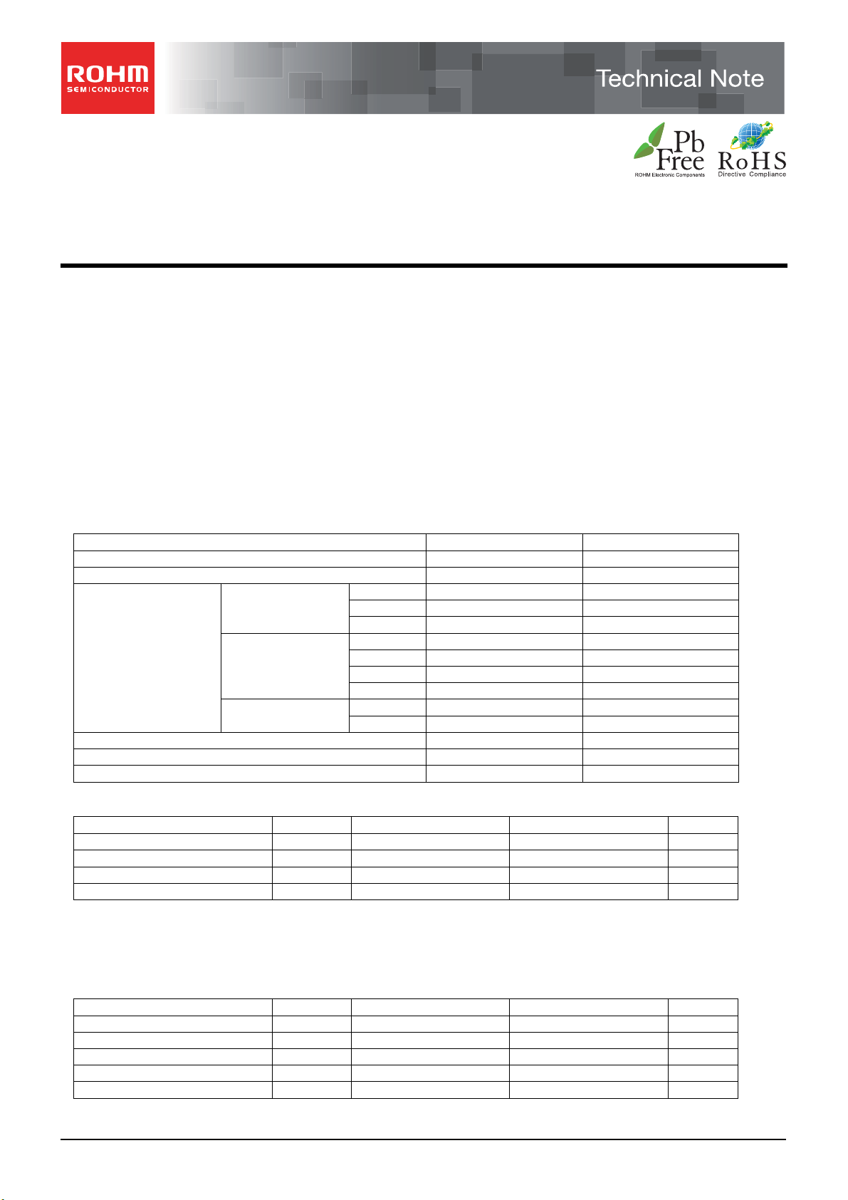
●Reference data (BU2285FV basic data)
Technical Note
RBW=1KHz
VBW=100Hz
1.0V / div
5.0nsec / div
Fig.1 54MHz output waveform
VDD=3.3V, at CL=15pF
1.0V / div
5.0nsec / div
Fig.4 27MHz output waveform
VDD=3.3V, at CL=15pF
1.0V / div
500psec / div
Fig.2 54MHz Period-Jitter
VDD=3.3V, at CL=15pF
1.0V / div
500psec / div
Fig.5 27MHz Period-Jitter
VDD=3.3V, at CL=15pF
10dB / div
10KHz / div
Fig.3 54MHz Spectrum
VDD=3.3V, at CL=15pF
RBW=1KHz
VBW=100Hz
10dB / div
10KHz / div
Fig.6 27MHz Spectrum
VDD=3.3V at CL=15pF
RBW=1KHz
VBW=100Hz
1.0V / div
10.0nsec / div
Fig.7 13.5MHz output waveform
VDD=3.3V, at CL=15pF
1.0V / div
5.0nsec / div
Fig.10 33.9MHz output waveform
VDD=3.3V, at CL=15pF
1.0V / div
500psec / div
Fig.8 13.5MHz Period-Jitter
VDD=3.3V, at CL=15pF
1.0V / div
500psec / div
Fig.11 33.9MHz Period-Jitter
VDD=3.3V, at CL=15pF
10dB / div
10KHz / div
Fig.9 13.5MHz Spectrum
VDD=3.3V, at CL=15pF
RBW=1KHz
VBW=100Hz
10dB / div
10KHz / div
Fig.12 33.9MHz Spectrum
VDD=3.3V, at CL=15pF
www.rohm.com
© 2009 ROHM Co., Ltd. All rights reserved.
4/16
2009.04 - Rev.
Page 5
A
BU2285FV,BU2363FV
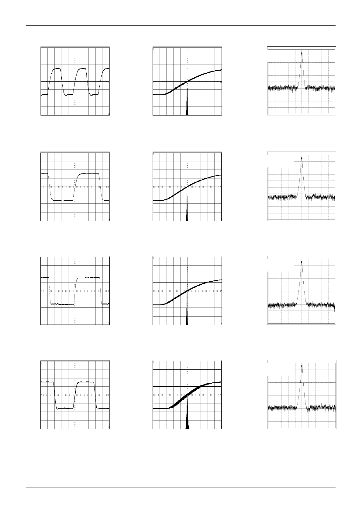
●Reference data (BU2285FV basic data)
Technical Note
RBW=1KHz
VBW=100Hz
1.0V / div
10.0nsec / div
Fig.13 16.9MHz output waveform
VDD=3.3V, at CL=15pF
1.0V / div
5.0nsec / div
Fig.16 36.9MHz output waveform
VDD=3.3V, at CL=15pF
1.0V / div
500psec / div
Fig.14 16.9MHz Period-Jitter
VDD=3.3V, at CL=15pF
1.0V / div
500psec / div
Fig.17 36.9MHz Period-Jitter
VDD=3.3V, at CL=15pF
10dB / div
10KHz / div
Fig.15 16.9MHz Spectrum
VDD=3.3V, at CL=15pF
RBW=1KHz
VBW=100Hz
10dB / div
10KHz / div
Fig.18 36.9MHz Spectrum
VDD=3.3V, at CL=15pF
RBW=1KHz
VBW=100Hz
1.0V / div
10.0nsec / div
Fig.19 18.4MHz output waveform
VDD=3.3V, at CL=15pF
1.0V / div
500psec / div
Fig.20 18.4MHz Period-Jitter
VDD=3.3V, at CL=15pF
10dB / div
10KHz / div
Fig.21 18.4MHz Spectrum
VDD=3.3V, at CL=15pF
www.rohm.com
© 2009 ROHM Co., Ltd. All rights reserved.
5/16
2009.04 - Rev.
Page 6
A
BU2285FV,BU2363FV
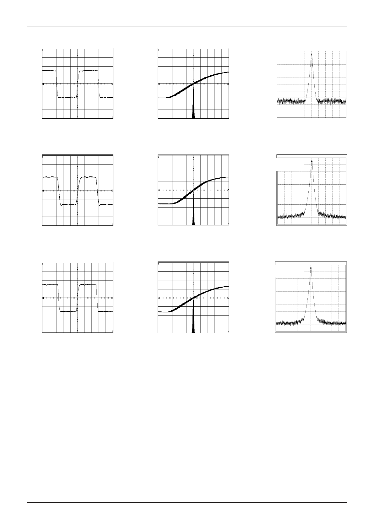
●Reference data (BU2285FV Temperature and Supply voltage variations data)
55
54
53
52
]
%
51
50
Duty[
:
49
Duty
48
47
46
45
-25 0 25 50 75 100
55
54
53
52
]
%
51
50
Duty[
:
49
Duty
48
47
46
45
-25 0 25 50 75 100
Temperature:T[℃]
Fig.22 54MHz
Temperature-Duty
Temperature:T[℃]
Fig.25 27MHz
Temperature-Duty
55
54
53
]
52
%
51
50
Duty[
:
49
Duty
48
47
46
45
-25 0 25 50 75 100
Temperature:T[℃]
VDD=3.3V
VDD=3.7V
VDD=2.9V
Fig.28 13.5MHz
Temperature-Duty
VDD=3.7V
VDD=3.3V
VDD=2.9V
VDD=3.7V
VDD=3.3V
VDD=2.9V
100
90
80
70
60
PJ-1σ [psec]
:
50
40
30
20
Period-jitter1σ
10
0
-25 0 25 50 75 100
Temperature:T[℃]
VDD=3.7V
VDD=3.3V
Fig.23 54MHz
Temperature-Period-Jitter 1σ
100
90
80
70
60
PJ-1σ [psec]
:
50
40
30
20
Period-jitter1σ
10
0
-25 0 25 50 75 100
Temperature:T[℃]
VDD=3.7V
VDD=3.3V
VDD=2.9V
Fig.26 27MHz
Temperature-Period-Jitter 1σ
100
90
80
70
60
PJ-1σ[psec]
:
50
40
30
20
Period-jitt er1σ
10
0
-25 0 25 50 75 100
Temperature:T[℃]
VDD=3.7V
VDD=3.3V
VDD=2.9V
Fig.29 13.5MHz
Temperature-Period-Jitter 1σ
Technical Note
600
:
500
400
300
200
PJ-MIN-MAX[psec]
100
Period-jitterMIN-MAX
0
-25 0 25 50 75 100
Temperature:T[℃]
Fig.24 54MHz
Temperature-Period-Jitter MIN-MAX
600
500
:
400
300
200
PJ-M IN -MAX[ psec]
Period-jitt erMI N-MAX
100
0
-25 0 25 50 75 100
Temperature:T[℃]
Fig.27 27MHz
Temperature-Period-Jitter MIN-MAX
600
500
:
400
300
200
PJ-M IN -MAX[ ps ec]
Period-jitterMI N-M AX
100
0
-25 0 25 50 75 100
Temperature:T[℃]
Fig.30 13.5MHz
Temperature-Period-Jitter MIN-MAX
VDD=2.9V
VDD=3.3V
VDD=3.7V VDD=2.9V
VDD=2.9V
VDD=3.3V
VDD=3.7V
VDD=3.7V
VDD=3.3V
VDD=2.9V
55
54
53
52
%]
51
50
Duty[
:
49
48
Duty
47
46
45
-25 0 25 50 75 100
VDD=2.9V
VDD=3.3V
VDD=3.7V
Temperature:T[℃]
Fig.31 33.9MHz
Temperature-Duty
www.rohm.com
© 2009 ROHM Co., Ltd. All rights reserved.
100
90
80
70
60
PJ-1σ[psec]
:
50
40
30
20
Period-jitt er1σ
10
0
-25 0 25 50 75 100
Temperature:T[℃]
VDD=2.9V
VDD=3.7V
VDD=3.3V
Fig.32 33.9MHz
Temperature-Period-Jitter 1σ
6/16
600
500
:
400
300
Period-jitterMI N-MAX
200
PJ-M IN -MAX[ps ec]
100
0
-25 0 25 50 75 100
Temperature:T[℃]
VDD=2.9V
VDD=3.7V
VDD=3.3V
Fig.33 33.9MHz
Temperature-Period-Jitter MIN-MAX
2009.04 - Rev.
Page 7

A
BU2285FV,BU2363FV
Technical Note
●Reference data (BU2285FV Temperature and Supply voltage variations data)
55
54
53
]
52
%
51
50
Duty[
:
49
Duty
48
47
46
45
-25 0 25 50 75 100
55
54
53
]
52
%
51
50
Duty[
:
49
Duty
48
47
46
45
-25 0 25 50 75 100
55
54
53
]
52
%
51
50
Duty[
:
49
Duty
48
47
46
45
-25 0 25 50 75 100
50
40
IDD[mA]
:
30
20
10
Circ uit C urrent
0
-25 0 25 50 75 100
Fig.43 Consumption current
(with maximum output load)
Temperature-Consumption current
Temperature:T[℃]
Fig.34 16.9MHz
Temperature-Duty
Temperature:T[℃]
Fig.37 36.9MHz
Temperature-Duty
Temperature:T[℃]
Fig.40 18.4MHz
Temperature-Duty
Temperature:T[℃]
VDD=2.9V
VDD=3.3V
VDD=3.7V
VDD=3.7V
VDD=3.3V
VDD=2.9V
VDD=2.9V
VDD=3.3V
VDD=3.7V
VDD=3.7V
VDD=3.3V
VDD=2.9V
100
90
80
70
60
PJ-1σ [psec]
:
50
40
30
20
Period-jitter1σ
10
0
-25 0 25 50 75 100
Temperature:T[℃]
VDD=2.9V
VDD=3.3V
VDD=3.7V
Fig.35 16.9MHz
Temperature-Period-Jitter 1σ
100
90
80
70
60
PJ-1σ [psec]
:
50
40
30
20
Period-jitt er1σ
10
0
-25 0 25 50 75 100
Temperature:T[℃]
VDD=2.9V
VDD=3.3V
VDD=3.7V
Fig.38 36.9MHz
Temperature-Period-Jitter 1σ
100
90
80
70
60
PJ-1σ [psec]
:
50
40
30
20
Period-jitt er1σ
10
0
-25 0 25 50 75 100
Temperature:T[℃]
VDD=3.3V
VDD=2.9V
VDD=3.7V
Fig.41 18.4MHz
Temperature-Period-Jitter 1σ
600
500
:
400
300
Period-jitt erMI N-MAX
200
PJ-M IN -MAX[ ps ec]
100
0
-25 0 25 50 75 100
Temperature:T[℃]
VDD=2.9V
VDD=2.9V
VDD=3.3V
VDD=3.3V
VDD=3.7V
VDD=3.7V
Fig.36 16.9MHz
Temperature-Period-Jitter MIN-MAX
600
500
:
400
300
200
PJ-M IN -MAX[ ps ec]
Period-jitt erMI N-MAX
100
0
-25 0 25 50 75 100
Temperature:T[℃]
VDD=2.9V
VDD=3.3V
VDD=3.7V
Fig.39 36.9MHz
Temperature-Period-Jitter MIN-MAX
600
500
:
VDD=2.9V
VDD=3.3V
VDD=3.7V
Period-jitt erMI N-MAX
400
300
200
PJ-M IN -MAX[ ps ec]
100
0
-25 0 25 50 75 100
Temperature:T[℃]
Fig.42 18.4MHz
Temperature-Period-Jitter MIN-MAX
www.rohm.com
© 2009 ROHM Co., Ltd. All rights reserved.
7/16
2009.04 - Rev.
Page 8

A
BU2285FV,BU2363FV
●Reference data (BU2363FV basic data)
Technical Note
RBW=1KHz
VBW=100Hz
1.0V / div
3.0nsec / div
Fig.44 54MHz output waveform
VDD=3.3V, at CL=15pF
1.0V / div
5.0nsec / div
Fig.47 27MHz output waveform
VDD=3.3V, at CL=15pF
1.0V / div
500psec / div
Fig.45 54MHz Period-Jitter
VDD=3.3V, at CL=15pF
1.0V / div
500psec / div
Fig.48 27MHz Period-Jitter
VDD=3.3V, at CL=15pF
10dB / div
10KHz / div
Fig.46 54MHz Spectrum
VDD=3.3V, at CL=15pF
RBW=1KHz
VBW=100Hz
10dB / div
10KHz / div
Fig.49 27MHz Spectrum
VDD=3.3V, at CL=15pF
RBW=1KHz
VBW=100Hz
1.0V / div
5.0nsec / div
Fig.50 33.9MHz output waveform
VDD=3.3V, at CL=15pF
1.0V / div
10.0nsec / div
Fig.53 16.9MHz output waveform
VDD=3.3V, at CL=15pF
1.0V / div
500psec / div
Fig.51 33.9MHz Period-Jitter
VDD=3.3V, at CL=15pF
1.0V / div
500psec / div
Fig.54 16.9MHz Period-Jitter
VDD=3.3V, at CL=15pF
10dB / div
10KHz / div
Fig.52 33.9MHz Spectrum
VDD=3.3V, at CL=15pF
RBW=1KHz
VBW=100Hz
10dB / div
10KHz / div
Fig.55 16.9MHz Spectrum
VDD=3.3V, at CL=15pF
www.rohm.com
© 2009 ROHM Co., Ltd. All rights reserved.
8/16
2009.04 - Rev.
Page 9

A
BU2285FV,BU2363FV
●Reference data (BU2363FV basic data)
1.0V / div
1.0V / div
Fig.56 36.9MHz output waveform
5.0nsec / div
VDD=3.3V, at CL=15pF
Fig.57 36.9MHz Period-Jitter
500psec / div
VDD=3.3V, at CL=15pF
1.0V / div
1.0V / div
Fig.59 18.4MHz output waveform
10.0nsec / div
VDD=3.3V, at CL=15pF
500psec / div
Fig.60 18.4MHz Period-Jitter
VDD=3.3V, at CL=15pF
●Reference data (BU2363FV Temperature and Supply voltage variations data)
55
54
53
52
51
50
Duty[%]
:
49
48
Duty
47
46
45
-25 0 25 50 75 100
55
54
53
52
51
50
Duty[%]
:
49
Duty
48
47
46
45
Temperature:T[℃]
Fig.62 54MHz
Temperature-Duty
-25 0 25 50 75 100
Temperature:T[℃]
Fig.65 27MHz
Temperature-Duty
VDD=3.7V
VDD=3.3V
VDD=2.9V
VDD=3.7V
VDD=3.3V
VDD=2.9V
100
90
80
70
60
PJ-1σ [psec]
:
50
40
30
20
Period-jitter1σ
10
0
-25 0 25 50 75 100
Temperature:T[℃]
VDD=3.7V
VDD=3.3V
VDD=2.9V
Fig.63 54MHz
Temperature-Period-Jitter 1σ
100
90
80
70
60
PJ-1σ [psec]
:
50
40
30
20
Period-jitt er1σ
10
0
-25 0 25 50 75 100
Temperature:T[℃]
VDD=3.3V
VDD=2.9V
VDD=3.7V
Fig.66 27MHz
Temperature-Period-Jitter 1σ
Technical Note
RBW=1KHz
VBW=100Hz
10dB / div
10KHz / div
Fig.58 36.9MHz Spectrum
VDD=3.3V, at CL=15pF
RBW=1KHz
VBW=100Hz
10dB / div
10KHz / div
Fig.61 18.4MHz Spectrum
VDD=3.3V, at CL=15pF
600
500
:
400
300
200
PJ-M IN -MAX[ psec]
Period-jitt erMI N-MAX
100
0
-25 0 25 50 75 100
Temperature:T[℃]
Fig.64 54MHz
Temperature-Period-Jitter MIN-MAX
600
500
:
400
300
200
PJ-M IN -MAX[ ps ec]
Period-jitterMI N-M AX
100
0
-25 0 25 50 75 100
Temperature:T[℃]
Fig.67 27MHz
Temperature-Period-Jitter MIN-MAX
VDD=2.9V
VDD=3.3V
VDD=3.7V
VDD=2.9V
VDD=3.3V
VDD=3.7V
www.rohm.com
© 2009 ROHM Co., Ltd. All rights reserved.
9/16
2009.04 - Rev.
Page 10

A
BU2285FV,BU2363FV
●Reference data (BU2363FV Temperature and Supply voltage variations data)
55
54
53
52
]
51
50
Duty[%
:
49
Duty
48
47
46
45
-25 0 25 50 75 100
Temperature:T[℃]
Fig.68 33.9MHz
Temperature-Duty
55
54
53
52
51
50
Duty[%]
:
49
Duty
48
47
46
45
-25 0 25 50 75 100
Temperature:T[℃]
Fig.71 16.9MHz
Temperature-Duty
VDD=3.7V
VDD=3.3V
VDD=2.9V
VDD=3.7V
VDD=3.3V
VDD=2.9V
100
90
80
70
60
PJ-1σ [psec]
:
50
40
30
20
Period-jitt er1σ
10
0
-25 0 25 50 75 100
Temperature:T[℃]
VDD=3.3V
VDD=3.7V
VDD=2.9V
Fig.69 33.9MHz
Temperature-Period-Jitter 1σ
100
90
80
70
60
PJ-1σ[psec]
:
50
40
30
20
Period-jitter1σ
10
0
-25 0 25 50 75 100
Temperature:T[℃]
VDD=3.7V
VDD=3.3V
VDD=2.9V
Fig.72 16.9MHz
Temperature-Period-Jitter 1σ
Technical Note
600
500
:
400
300
200
PJ-M IN -MAX[ psec]
Period-jitt erMI N-MAX
100
0
-25 0 25 50 75 100
Temperature:T[℃]
Fig.70 33.9MHz
Temperature-Period-Jitter MIN-MAX
600
500
:
400
300
200
PJ-M IN -MAX[ psec]
Period-jitt erMI N-MAX
100
0
-25 0 25 50 75 100
Temperature:T[℃]
Fig.73 16.9MHz
Temperature-Period-Jitter
VDD=3.7V
VDD=3.3V
VDD=2.9V
VDD=3.7V
VDD=3.3V
VDD=2.9V
55
54
53
52
51
50
Duty[%]
:
49
Duty
48
47
46
45
-25 0 25 50 75 100
Temperature:T[℃]
VDD=3.7V VDD=2.9V
VDD=3.3V
VDD=2.9V
Fig.74 36.9MHz
Temperature-Duty
55
54
53
52
51
50
Duty[%]
:
49
Duty
48
47
46
45
-25 0 25 50 75 100
Temperature:T[℃]
VDD=3.7V
VDD=3.3V
VDD=2.9V
Fig.77 18.4MHz
Temperature-Duty
100
90
80
70
60
PJ-1σ [psec]
:
50
40
30
20
Period-jitt er1σ
10
0
-25 0 25 50 75 100
VDD=3.3V
VDD=3.7V
Temperature:T[℃]
Fig.75 36.9MHz
Temperature-Period-Jitter 1σ
100
90
80
70
60
PJ-1σ [psec]
:
50
40
30
20
Period-jitt er1σ
10
0
-25 0 25 50 75 100
Temperature:T[℃]
VDD=2.9V
VDD=3.3V
VDD=3.7V
Fig.78 18.4MHz
Temperature-Period-Jitter 1σ
600
500
:
400
300
200
PJ-M IN -MAX[ psec]
Period-jitt erMI N-MAX
100
0
-25 0 25 50 75 100
Temperature:T[℃]
VDD=3.3V
VDD=2.9V
VDD=3.7V
Fig.76 36.9MHz
Temperature-Period-Jitter MIN-MAX
600
:
Period-jitterMI N-MAX
500
400
300
200
PJ-M IN -MAX[ ps ec]
100
0
-25 0 25 50 75 100
Temperature:T[℃]
VDD=3.3V
VDD=2.9V
VDD=3.7V
Fig.79 18.4MHz
Temperature-Period-Jitter
www.rohm.com
© 2009 ROHM Co., Ltd. All rights reserved.
10/16
2009.04 - Rev.
Page 11

A
BU2285FV,BU2363FV
●Reference data (BU2363FV Temperature and Supply voltage variations data)
50
40
IDD[mA]
:
30
20
10
Circ uit C urrent
0
-25 0 25 50 75 100
Fig.80 Consumption current
(with maximum output load)
Temperature-Consumption current
VDD=3.7V
VDD=3.3V
VDD=2.9V
Temperature:T[℃]
●Block diagram, Pin assignment
◎BU2285FV
23:CTRLB
8:XTALIN
9:XTALOUT
(CTRLB=OPEN:27.0000MHz
CTRL=L :13.5000MHz)
XTAL
OSC
PLL1
PLL2
1/2
1/4
1/8
1/4
22:CLK54M
16:CLK27M
20:CLKDAC
24:CLK33M
1/8
3:CLK16M
12:CLKA
21:OE
11:CTRA
(CTRLA=OPEN:48.0kHz type
CTRLA=L :44.1kHz type)
1/2
13:CLKB
Fig.81
1:VDD1 24:CLK33M
2:VSS1 23:CTRLB
3:CLK16M 22:CLK54M
4:AVSS 21:OE
5:AVDD 20:CLKDAC
6:AVDD 19:DVDD
7:AVSS 18:DVSS
8:XTALIN 17:DVSS
9:XTALOUT 16:CLK27M
10:NC 15:VDD2
11:CTRLA 14:VSS2
12:CLKA 13:CLKB
BU2285FV
CTRLA CLKA CLKB
L 33.8688MHz 16.9344MHz
OPEN 36.8640MHz 18.4320MHz
CTRLB CLKDAC
L 13.5000MHz
OPEN 27.0000MHz
Fig.82
(54.0000MHz)
(27.0000MHz)
(CTRLB=OPEN:27.0000MHz
CTRLB=L :13.5000MHz)
(33.8688MHz )
(16.9344MHz)
(CTRLA=OPEN:36.8640MHz
CTRLA=L :33.8688MHz)
(CTRLA=OPEN:18.4320MHz
CTRLA=L :16.9344MHz)
Technical Note
www.rohm.com
© 2009 ROHM Co., Ltd. All rights reserved.
11/16
2009.04 - Rev.
Page 12

A
BU2285FV,BU2363FV
●Block diagram, Pin assignment
◎BU2363FV
Technical Note
7:XTALIN
8:XTALOUT
16:OE
14:FSEL
XTALIN=36.8640MHz
XTAL
OSC
(FSEL=OPEN:48.0kHz type
FSEL=L :44.1kHz type)
MULTI-PLL
Technology
PLL2
1/2
Fig.83
1/4
1/8
1/4
1/8
3:CLK54M
(54.0000MHz)
4:CLK27M
(27.0000MHz)
15:CLK33M
(33.8688MHz)
13:CLK16M
(16.9344MHz)
10:768FS1
(FSEL=OPEN:36.8640MHz
FSEL=L :33.8688MHz)
9:384FS2
(FSEL=OPEN:18.4320MHz
FSEL=L :16.9344MHz)
1:VDD2 16:OE
2:VSS2 15:CLK33M
3:CLK254M 14:FSEL
4:CLK27M 13:CLK16M
5:AVDD 12:DVDD
6:AVSS 11:DVSS
7:XTALIN 10:768FS1
8:XTALOUT 9:384FS2
BU2363FV
Fig.84
FSEL CLK768FS CLK384FS
L 33.8688MHz 16.9344MHz
OPEN 36.8640MHz 18.4320MHz
www.rohm.com
© 2009 ROHM Co., Ltd. All rights reserved.
12/16
2009.04 - Rev.
Page 13

A
BU2285FV,BU2363FV
●Example of application circuit
◎BU2285FV
0.1uF
16.9344MHz
1:VDD1 24:CLK33M
2:VSS1 23: CTRLB
3:CLK16M 22:CLK54M
0.1uF L :Disable
0.1uF 0.1uF
OPEN:48.0kHz type
L :44.1kHz type 11: CTRLA 14:VSS2
36.8640MHz
or 33.8688MHz or 16.9344MHz
4:AVSS 21:OE
5:AVDD 20:CLKDAC
6:AVDD 19:DVDD
7:AVSS 18:DVSS
8:XTALIN 17:DVSS
9:XTALOUT 16:CLK27M
10:NC 15:VDD2
12:CLKA 13:CLKB
BU2285FV
Fig.85
Pin Function
PIN No. PIN Name PIN Function
1 VDD1 33MHz system power supply
2 VSS1 33MHz system GND
3 CLK16M 16.9344MHz output
4 AVSS Analog GND
5 AVDD Analog power supply
6 AVDD Analog power supply
7 AVSS Analog GND
8 XTALIN Crystal input terminal
9 XTALOUT Crystal output terminal
10 NC NC
11 CTRLA CLKA or B output selection (with pull-up)
12 CLKA CTRLA=OPEN:36.8640MHz, CTRLA=L:33.8688MHz
13 CLKB CTRLA=OPEN:18.4320MHz, CTRLA=L:16.9344MHz
14 VSS2 CLKA, B GND
15 VDD2 CLKA, B power supply
16 CLK27M 27.0000MHz output
17 DVSS Digital GND
18 DVSS Digital GND
19 DVDD Digital power supply
20 CLKDAC CTRLB=OPEN:27.0000MHz, CTRLB=L:13.5000MHz
21 OE Output enable (with pull-up), OPEN:enable, L:disable
22 CLK54M 54.0000MHz output
23 CTRLB CLKDAC output selection(with pull-up)
24 CLK33M 33.8688MHz output
Note) Basically, mount ICs to the printed circuit board for use.
(If the ICs are not mounted to the printed circuit board, the characteristics of ICs may not be fully demonstrated.)
Mount 0.1F capacitors in the vicinity of the IC PINs between 1PIN (VDD1) and 2PIN (VSS1), 4PIN (AVSS) and 5PIN (AVDD), 6PIN (AVDD) and 7PIN
(AVSS), 14PIN (VSS2) and 15PIN (VDD2), and 17PIN/18PIN (DVSS) and 19PIN (DVDD), respectively.
Depending on the conditions of the printed circuit board, mount an additional electrolytic capacitor between the power supply and GND terminal.
For EMI protection, it is effective to put ferrite beads in the origin of power supply to be fed to BU2285FV from the printed circuit board or to insert a
capacitor (of 1 or less), which bypasses high frequency desired, between the power supply and the GND terminal.
Technical Note
33.8688MHz
OPEN:27.0000MHz
L :13.5000MHz
54.0000MHz
OPEN:Enable
27.0000MHz
or 13.5000MHz
27.0000MHz
0.1uF
18.4320MHz
www.rohm.com
© 2009 ROHM Co., Ltd. All rights reserved.
13/16
2009.04 - Rev.
Page 14

A
BU2285FV,BU2363FV
●Example of application circuit
◎BU2363FV
0.1uF
54.0000MHz
27.0000MHz
0.1uF 0.1uF
1:VDD2 16:OE
2:VSS2 15:CLK33M
3:CLK254M 14:FSEL
4:CLK27M 13:CLK16M
5:AVDD 12:DVDD
6:AVSS 11:DVSS
7:XTALIN 10:768FS1
8:XTALOUT 9:384FS2
BU2363FV
Fig.86
Pin Function
PIN No. PIN Name PIN Function
1 VDD2 27MHz, 54MHz power supply
2 VSS2 27MHz, 54MHzGND
3 CLK54M 54.0000MHz output
4 CLK27M 27.0000MHz output
5 AVDD Analog power supply
6 AVSS Analog GND
7 XTALIN Crystal input terminal
8 XTALOUT Crystal output terminal
9 384FS2 FSEL=OPEN:18.4320MHz, FSEL=L:16.9344MHz
10 768FS1 FSEL=OPEN:36.8640MHz, FSEL=L:33.8688MHz
11 DVSS Digital GND
12 DVDD Digital power supply
13 CLK16M 16.9344MHz output
9, 10PIN output selection(with pull-up)
14 FSEL
OPEN:18.4320MHz(9PIN), 36.8640MHz(10PIN)
L:16.9344MHz(9PIN), 33.8688MHz(10PIN)
15 CLK33M 33.8688MHz output
16 OE Output enable (with pull-up), OPEN:enable, L:disable
Note) Basically, mount ICs to the printed circuit board for use.
(If the ICs are not mounted to the printed circuit board, the characteristics of ICs may not be fully demonstrated.)
Mount 0.1F capacitors in the vicinity of the IC PINs between 1PIN (VDD2) and 2PIN (VSS2), 5PIN (AVDD) and 6PIN (AVSS), 11PIN (DVSS) and 12PIN
(DVDD), respectively.
Depending on the conditions of the printed circuit board, mount an additional electrolytic capacitor between the power supply and GND terminal.
For EMI protection, it is effective to put ferrite beads in the origin of power supply to be fed to BU2363FV from the printed circuit board or to insert a
capacitor (of 1 or less), which bypasses high frequency desired, between the power supply and the GND terminal.
Even though we believe that the example of recommended circuit is worth of a recommendation, please be sure to thoroughly recheck the characteristics
before use.
Technical Note
OPEN:Enable
L :Disable
33.8688MHz
OPEN:48.0kHz type
L :44.1kHz type
16.9344MHz
36.8640MHz
or 33.8688MHz
18.4320MHz
or 16.9344MHz
www.rohm.com
© 2009 ROHM Co., Ltd. All rights reserved.
14/16
2009.04 - Rev.
Page 15

A
BU2285FV,BU2363FV
●Notes for use
(1) Absolute Maximum Ratings
An excess in the absolute maximum ratings, such as applied voltage (VDD or VIN), operating temperature range (Topr),
etc., can break down devices, thus making impossible to identify breaking mode such as a short circuit or an open circuit.
If any special mode exceeding the absolute maximum ratings is assumed, consideration should be given to take physical
safety measures including the use of fuses, etc.
(2) Recommended operating conditions
These conditions represent a range within which characteristics can be provided approximately as expected. The
electrical characteristics are guaranteed under the conditions of each parameter.
(3) Reverse connection of power supply connector
The reverse connection of power supply connector can break down ICs. Take protective measures against the breakdown
due to the reverse connection, such as mounting an external diode between the power supply and the IC’s power supply
terminal.
(4) Power supply line
Design PCB pattern to provide low impedance for the wiring between the power supply and the GND lines.
In this regard, for the digital block power supply and the analog block power supply, even though these power supplies has
the same level of potential, separate the power supply pattern for the digital block from that for the analog block, thus
suppressing the diffraction of digital noises to the analog block power supply resulting from impedance common to the
wiring patterns. For the GND line, give consideration to design the patterns in a similar manner.
Furthermore, for all power supply terminals to ICs, mount a capacitor between the power supply and the GND terminal. At
the same time, in order to use an electrolytic capacitor, thoroughly check to be sure the characteristics of the capacitor to be
used present no problem including the occurrence of capacity dropout at a low temperature, thus determining the constant.
(5) GND voltage
Make setting of the potential of the GND terminal so that it will be maintained at the minimum in any operating state.
Furthermore, check to be sure no terminals are at a potential lower than the GND voltage including an actual electric transient.
(6) Short circuit between terminals and erroneous mounting
In order to mount ICs on a set PCB, pay thorough attention to the direction and offset of the ICs. Erroneous mounting can
break down the ICs. Furthermore, if a short circuit occurs due to foreign matters entering between terminals or between
the terminal and the power supply or the GND terminal, the ICs can break down.
(7) Operation in strong electromagnetic field
Be noted that using ICs in the strong electromagnetic field can malfunction them.
(8) Inspection with set PCB
On the inspection with the set PCB, if a capacitor is connected to a low-impedance IC terminal, the IC can suffer stress.
Therefore, be sure to discharge from the set PCB by each process. Furthermore, in order to mount or dismount the set
PCB to/from the jig for the inspection process, be sure to turn OFF the power supply and then mount the set PCB to the jig.
After the completion of the inspection, be sure to turn OFF the power supply and then dismount it from the jig. In addition,
for protection against static electricity, establish a ground for the assembly process and pay thorough attention to the
transportation and the storage of the set PCB.
(9) Input terminals
In terms of the construction of IC, parasitic elements are inevitably formed in relation to potential. The operation of the
parasitic element can cause interference with circuit operation, thus resulting in a malfunction and then breakdown of the
input terminal. Therefore, pay thorough attention not to handle the input terminals, such as to apply to the input terminals a
voltage lower than the GND respectively, so that any parasitic element will operate. Furthermore, do not apply a voltage to
the input terminals when no power supply voltage is applied to the IC. In addition, even if the power supply voltage is
applied, apply to the input terminals a voltage lower than the power supply voltage or within the guaranteed value of
electrical characteristics.
(10) Ground wiring pattern
If small-signal GND and large-current GND are provided, It will be recommended to separate the large-current GND
pattern from the small-signal GND pattern and establish a single ground at the reference point of the set PCB so that
resistance to the wiring pattern and voltage fluctuations due to a large current
small-signal GND. Pay attention not to cause fluctuations in the GND wiring pattern of external parts as well.
(11) External capacitor
In order to use a ceramic capacitor as the external capacitor, determine the constant with consideration given to a
degradation in the nominal capacitance due to DC bias and changes in the capacitance due to temperature, etc.
will cause no fluctuations in voltages of the
Technical Note
www.rohm.com
© 2009 ROHM Co., Ltd. All rights reserved.
15/16
2009.04 - Rev.
Page 16

A
BU2285FV,BU2363FV
●Ordering part number
Technical Note
B U
Part No. Part No.
SSOP-B24
7.8 ± 0.2
(MAX 8.15 include BURR)
24
7.6 ± 0.3
5.6 ± 0.2
1
1.15 ± 0.1
0.1
0.65
0.22 ± 0.1
SSOP-B16
5.0±0.2
16
4.4±0.2
6.4±0.3
1
2 2 8 5
2285
2363
13
0.3Min.
12
0.15 ± 0.1
0.1
(Unit : mm)
9
0.3Min.
8
0.15±0.1
F V - E 2
Package
FV:SSOP-B24
FV:SSOP-B16
<Tape and Reel information>
Embossed carrier tapeTape
Quantity
Direction
of feed
<Tape and Reel information>
Quantity
Direction
of feed
2000pcs
E2
The direction is the 1pin of product is at the upper left when you hold
()
reel on the left hand and you pull out the tape on the right hand
Reel
Embossed carrier tapeTape
2500pcs
E2
The direction is the 1pin of product is at the upper left when you hold
()
reel on the left hand and you pull out the tape on the right hand
Packaging and forming specification
E2: Embossed tape and reel
1pin
Order quantity needs to be multiple of the minimum quantity.
∗
Direction of feed
1.15±0.1
0.10
0.65
0.22±0.1
0.1
Direction of feed
(Unit : mm)
Reel
1pin
Order quantity needs to be multiple of the minimum quantity.
∗
www.rohm.com
© 2009 ROHM Co., Ltd. All rights reserved.
16/16
2009.04 - Rev.
Page 17

Notes
No copying or reproduction of this document, in part or in whole, is permitted without the
consent of ROHM Co.,Ltd.
The content specied herein is subject to change for improvement without notice.
The content specied herein is for the purpose of introducing ROHM's products (hereinafter
"Products"). If you wish to use any such Product, please be sure to refer to the specications,
which can be obtained from ROHM upon request.
Examples of application circuits, circuit constants and any other information contained herein
illustrate the standard usage and operations of the Products. The peripheral conditions must
be taken into account when designing circuits for mass production.
Great care was taken in ensuring the accuracy of the information specied in this document.
However, should you incur any damage arising from any inaccuracy or misprint of such
information, ROHM shall bear no responsibility for such damage.
The technical information specied herein is intended only to show the typical functions of and
examples of application circuits for the Products. ROHM does not grant you, explicitly or
implicitly, any license to use or exercise intellectual proper ty or other rights held by ROHM and
other par ties. ROHM shall bear no responsibility whatsoever for any dispute arising from the
use of such technical information.
Notice
The Products specied in this document are intended to be used with general-use electronic
equipment or devices (such as audio visual equipment, ofce-automation equipment, communication devices, electronic appliances and amusement devices).
The Products specied in this document are not designed to be radiation tolerant.
While ROHM always makes efforts to enhance the quality and reliability of its Products, a
Product may fail or malfunction for a variety of reasons.
Please be sure to implement in your equipment using the Products safety measures to guard
against the possibility of physical injury, re or any other damage caused in the event of the
failure of any Product, such as derating, redundancy, re control and fail-safe designs. ROHM
shall bear no responsibility whatsoever for your use of any Product outside of the prescribed
scope or not in accordance with the instruction manual.
The Products are not designed or manufactured to be used with any equipment, device or
system which requires an extremely high level of reliability the failure or malfunction of which
may result in a direct threat to human life or create a risk of human injury (such as a medical
instrument, transpor tation e quipment, aerospace machiner y, nuclear-reactor controller,
fuel-controller or other safety device). ROHM shall bear no responsibility in any way for use of
any of the Products for the above special purposes. If a Product is intended to be used for any
such special purpose, please contact a ROHM sales representative before purchasing.
If you intend to export or ship overseas any Product or technology specied herein that may
be controlled under the Foreign Exchange and the Foreign Trade Law, you will be required to
obtain a license or permit under the Law.
www.rohm.com
© 2009 ROHM Co., Ltd. All rights reserved.
Thank you for your accessing to ROHM product informations.
More detail product informations and catalogs are available, please contact us.
ROHM Customer Support System
http://www.rohm.com/contact/
R0039
A
 Loading...