

A
GPIO ICs
Keyencoder IC
BU1852GUW
No.11098EAT04
●Description
Keyencoder IC BU1852GUW can monitor up to 8x12 matrix (96 keys), which means to be adaptable to Qwerty keyboard.
We adopt the architecture that the information of the only key which status is changed, like push or release, is encoded into
the 8 bits data. This can greatly reduce the CPU load which tends to become heavier as the number of keys increase.
(Previously, all key's status is stored in the registers.) When the number of keys is small, the extra ports can be used as
GPIO. Furthermore, auto sleep function contributes to low power consumption, when no keys are pressed. It is also
equipped with the various functions such as ghost key rejection, N-key Rollover, Built-in power on reset and oscillator.
●Features
1) Monitor up to 96 matrix keys.
2) Under 3µA Stand-by Current
3) Built-in Power on Reset.
4) Ghost key rejection.
5) Keyscan / GPIO selectable
6) 3 volt tolerant Input
●Absolute maximum ratings (Ta=25℃)
Parameter Symbol Ratings Unit Conditions
VDD -0.3 ~ +2.5 V VDD≦VDDIO
Supply Voltage
VDDIO -0.3 ~ +4.5 V
1
※
VI1 -0.3 ~ VDD +0.3
V XRST, XI, TW, PORENB
1
Input voltage
VI2 -0.3 ~ VDDIO +0.3
※
V ADR
VIT -0.3 ~ +4.5 V
Storage temperature range Tstg -55 ~ +125 ℃
2
Package power PD 272
※ This IC is not designed to be X-ray proof.
※1 It is prohibited to exceed the absolute maximum ratings even including +0.3 V.
※2 Package dissipation will be reduced each 2.72mW/℃ when the ambient temperature increases beyond 25℃.
※
mW
●Operating conditions
Ratings
Parameter Symbol
Min. Typ. Max.
Supply voltage range
(VDD)
Supply voltage range
(VDDIO)
VDD 1.65 1.80 1.95 V
VDDIO 1.65 1.80 3.60 V
VI1 -0.2 - VDD+0.2 V XRST, XI, TW, PORENB
Input voltage range
VI2 -0.2 - VDDIO+0.2 V ADR
VIT -0.2 - 3.60 V
XINT, SCL, SDA,
COL[11:0], ROW[7:0]
Unit Conditions
XINT, SCL, SDA,
COL[11:0], ROW[7:0]
Operating temperature range Topr -30 25 +85 ℃
www.rohm.com
1/24
© 2011 ROHM Co., Ltd. All rights reserved.
2011.01 - Rev.

BU1852GUW
A
●Electrical characteristics
1. DC characteristics (VDD=1.8V, VDDIO=1.8V, Ta=25℃)
Parameter Symbol
Min. Typ. Max.
Input H Voltage1 V
Input H Voltage2 V
0.8xVDD - 3.6 V
IH1
0.8xVDD - VDD+0.2 V
IH2
Limits
Technical Note
Unit Conditions
1
※
2
※
Input H Voltage3 V
Input H Voltage4 V
Input L Voltage1 V
Input L Voltage2 V
Input H Current1 I
Input H Current2 I
0.8xVDDIO - 3.6 V COL[11:0]
IH3
0.8xVDDIO - VDDIO+0.2 V ADR
IH4
-0.2 - 0.2xVDD V
IL1
-0.2 - 0.2xVDDIO V ADR, COL[11:0]
IL2
-1.0 - 1.0 µA
IH1
-1.0 - 1.0 µA VIN=1.80V
IH2
Input L Current IIL -1.0 - 1.0 µA
Output H Voltage1 V
Output H Voltage2 V
Output L Voltage1 V
Output L Voltage2 V
※1 XINT,SCL,SDA,ROW[7:0]
※2 XRST,XI,TW,PORENB
※3 XINT,SCL,SDA,ROW[7:0],XRST,XI,TW,PORENB
※4 XINT,SCL,SDA,ROW[7:0],COL[11:0]
※5 XRST,XI,TW,PORENB,ADR
※6 XINT,SDA,ROW[7:0]
0.75xVDD - - V IOH=-2mA, ROW[7:0]
OH1
0.75xVDDIO - - V IOH=-2mA, COL[11:0]
OH2
- - 0.25xVDD V IOL=2mA,
OL1
- - 0.25xVDDIO V IOL=2mA, COL[11:0]
OL2
2. Circuit Current (VDD=1.8V, VDDIO=1.8V, Ta=25℃)
Limits
Parameter Symbol
Min. Typ. Max.
3
※
4
※
V
IN
=3.60V
Pull-down/up OFF
5
※
=0V
V
IN
Pull-down/up OFF
6
※
Unit Conditions
Power Down Current
(VDD)
- - 1.0 µA
I
PD
XRST=VSS
Power Down Current
(VDDIO)
Standby Current1
(VDD)
- - 1.0 µA
I
PDIO
I
- - 3.0 µA
STBY1
XRST=VDD,
PORENB=VSS,
Standby Current1
(VDDIO)
Standby Current2
(VDD)
- - 1.0 µA
I
STBYIO1
I
- - 1.0 µA
STBY2
SCL=VDD, SDA=VDD
XRST=VDD,
PORENB=VDD,
Standby Current2
(VDDIO)
Operating Current
(VDD)
I
- - 1.0 µA
STBYIO2
I
- 50 110 µA
OP
SCL=VDD, SDA=VDD
Internal oscillator is used.
one key is pressed.
www.rohm.com
2/24
© 2011 ROHM Co., Ltd. All rights reserved.
2011.01 - Rev.
BU1852GUW
A
Technical Note
2
C AC Characteristics
3. I
Condition
(Repeated)
START
tSU;STA
SCL
SDA
tHD;STA
tBUF
VDD=1.8V, VDDIO=1.8V, Topr=25℃, TW=VSS
Parameter Symbol
SCL Clock Frequency f
SCL
t
LOW
BIT7
tHIGH
BIT6
1/fSCLK
tSU;DAT
Fig.1 I
tHD;DAT
2
C AC timing
Ack
STOP
tSU;STO
Limits
Unit Conditions
Min. Typ. Max.
- - 400 kHz
Bus free time t
(Repeated) START Condition
Setup Time
(Repeated) START Condition
Hold Time
SCL Low Time t
SCL High Time t
Data Setup Time t
Data Hold Time t
STOP Condition Setup Time t
1.3 - - µs
BUF
t
0.6 - - µs
SU;STA
0.6 - - µs
t
HD;STA
1.3 - - µs
LOW
0.6 - - µs
HIGH
100 - - ns
SU;DAT
0 - - ns
HD;DAT
0.6 - - µs
SU;STO
www.rohm.com
3/24
© 2011 ROHM Co., Ltd. All rights reserved.
2011.01 - Rev.
BU1852GUW
A
4. GPIO AC Characteristics
GPIO[7:0](Output)
GPIO[7:0](Input)
VDD=1.8V, VDDIO=1.8V, Topr=25℃, TW=VSS
Output Data Valid Time tDV - - 0.8 µs
State
SCL
tIV
XINT
Fig.2 GPIO AC timing
Limits
Parameter Symbol
Min. Typ. Max.
BIT 0BIT 1
tDV
Unit Conditions
Technical Note
A
NA
t
IR
Interrupt Valid Time tIV - - 5 µs
Interrupt Reset Time tIR - - 5 µs
www.rohm.com
4/24
© 2011 ROHM Co., Ltd. All rights reserved.
2011.01 - Rev.
BU1852GUW
A
5. Startup sequence
VDD
VDDIO
tVDD
XRST
tVDD
SCL
SDA
VDD=1.8V, VDDIO=1.8V, Topr=25℃, TW=VSS
Parameter Symbol
VDD Stable Time t
Reset Wait Time t
VDD
RWAIT
tVDD
tRWAIT
tI2CWAIT
tRV
tI2CWAIT
Fig.3 Start Sequence timing
Limits
Unit Conditions
Min. Typ. Max.
- - 5 ms
VDD and VDDIO are ON
at the same time.
0 - - µs XRST controlling
Technical Note
tVDD
tRWAIT
1
※
Reset Valid Time tRV 10 - - µs
I2C Wait Time t
※1 Even if XRST port is not used, it operates because Power On Reset is built in.
In this case, connect XRST port with VDD on the set PCB.
10 - - µs
I2CWAIT
Note) At VDD=0V, when SCL port is changed from 0V to 0.5V or more, SCL port pulls the current. It is same in SDA, XINT,
and ROW[7:0] ports of 3V tolerant I/O. (VDDIO=0V in case of COL[11:0] ports)
VDD
Port
Port
0V
3V
0V
0.1~1mA
(~2kΩ Pull-up)
Pull Current
2~3ms
Fig.4 Port operating at VDD=0V
www.rohm.com
5/24
© 2011 ROHM Co., Ltd. All rights reserved.
2011.01 - Rev.
BU1852GUW
A
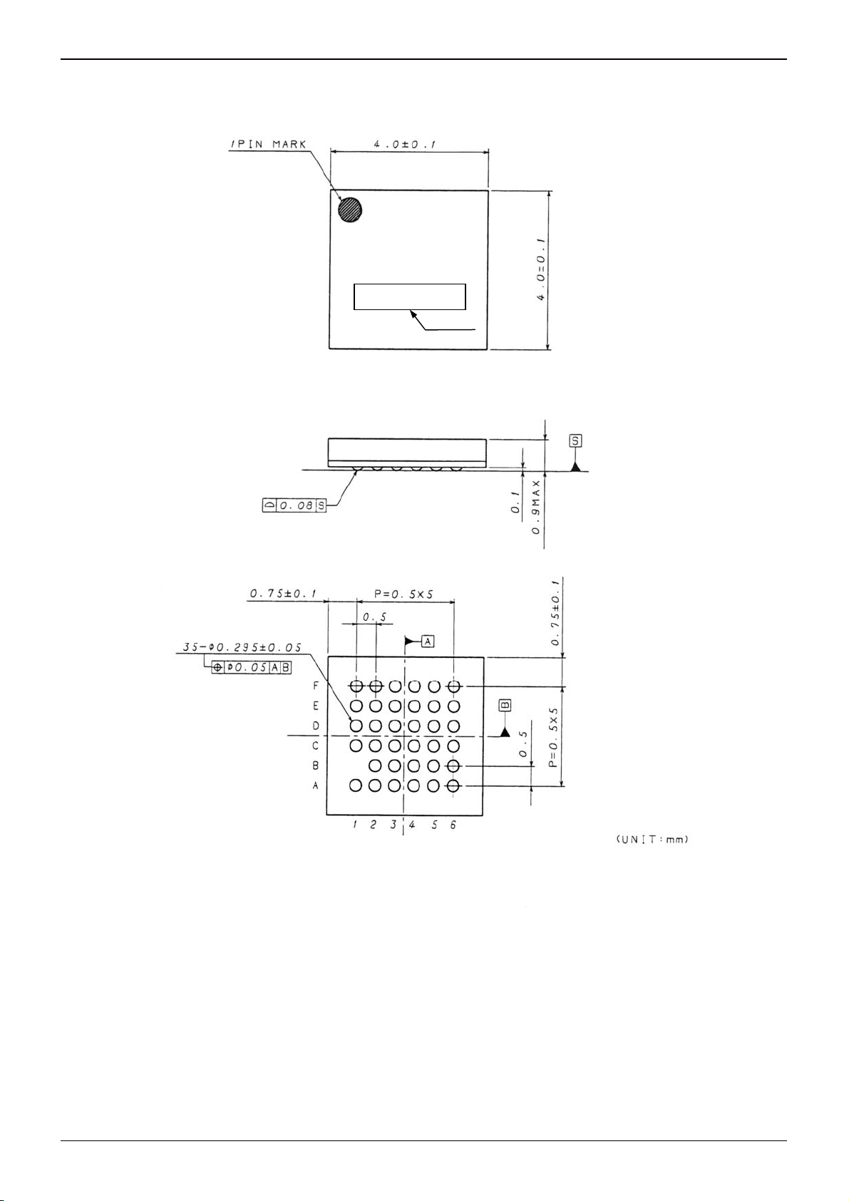
●Package Specification
Technical Note
U1852
Lot No.
Fig.5 Package Specification (VBGA035W040)
www.rohm.com
6/24
© 2011 ROHM Co., Ltd. All rights reserved.
2011.01 - Rev.
BU1852GUW
A
A
●Pin Assignment
Technical Note
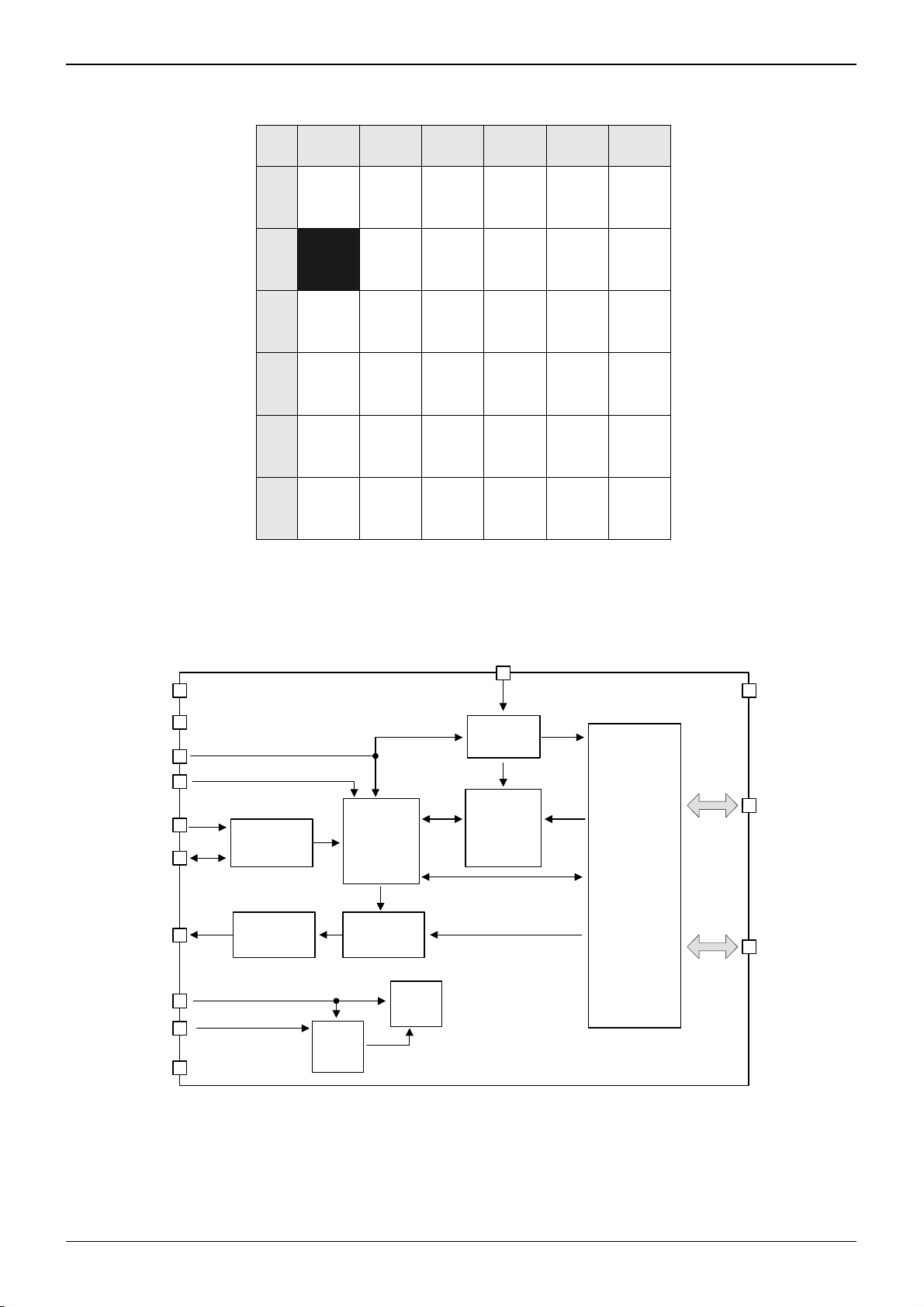
●Block diagram
VDD
TESTM[1:0]
ADR
TW
SCL
SDA
XINT
XRST
PORENB
VSS
A
B
C
D
E
F
Input
Filter
Interrupt
Filter
1 2 3 4 5
TESTM 0 XI ROW0 ROW2 ROW4
XRST ROW1 ROW3 ROW6
XINT VDD PORENB VSS ROW 7
SDA VDD VDDIO VSS COL2
SCL COL10 COL8 COL6 COL4
TESTM 1 COL11 COL9 COL7 COL5
Fig.6 Pin Diagram (Top View)
XI
Oscillator
Key
I2C / 3 wire
Control
Interrupt
Logic
Reset
Gen
Power
on
Reset
Fig.7 Functional Block Diagram
Encoder
+
FIFO
6
TW
ROW5
COL0
COL1
COL3
DR
VDDIO
COL[11:0]/
GPIO[19:8]
Key Scan
/
GPIO
Control
ROW[7:0]/
GPIO[7:0]
www.rohm.com
7/24
© 2011 ROHM Co., Ltd. All rights reserved.
2011.01 - Rev.

BU1852GUW
A
●Pin Functional Descriptions
PIN name I/O Function Init Cell Type
VDD - Power supply (Core, I/O except for COL[11:0], ADR) - -
VDDIO - Power supply (I/O for COL[11:0], ADR) - -
VSS - GND - -
XRST I Reset(Low Active) I A
XI I External clock input (32kHz) I I
Select protocol
TW I
H: original 3 wire
L: I
(TW=L) Select Device Address for I
ADR I
(TW=H) H : Key scan rate 1/2
2
C
2
C
I B
I B
L : Key scan rate original
XINT O Key/GPIO Interrupt
H(TW=H)
Hi-z(TW=L)
SCL I Clock for serial interface I D
SDA I/O Serial data inout for serial interface I F
ROW0 I/O ROW0 / GPIO0
Technical Note
E
ROW1 I/O ROW1 / GPIO1
ROW2 I/O ROW2 / GPIO2
ROW3 I/O ROW3 / GPIO3
ROW4 I/O ROW4 / GPIO4
ROW5 I/O ROW5 / GPIO5
ROW6 I/O ROW6 / GPIO6
ROW7 I/O ROW7 / GPIO7
COL0 I/O COL0 / GPIO8
COL1 I/O COL1 / GPIO9
COL2 I/O COL2 / GPIO10
COL3 I/O COL3 / GPIO11
COL4 I/O COL4 / GPIO12
COL5 I/O COL5 / GPIO13
COL6 I/O COL6 / GPIO14
COL7 I/O COL7 / GPIO15
COL8 I/O COL8 / GPIO16
COL9 I/O COL9 / GPIO17
I
[100kΩ Pull-up]
L(TW=H)
I
[150kΩ Pull-down]
(TW=L)
G
H
COL10 I/O COL10 / GPIO18
COL11 I/O COL11 / GPIO19
PORENB I Power on reset enable (Low Active) I B
TESTM0 I
Tes t P in s
1
※
I C
TESTM1 I
※1 Note: All these pins must be tied down to GND in normal operation.
www.rohm.com
8/24
© 2011 ROHM Co., Ltd. All rights reserved.
2011.01 - Rev.

BU1852GUW
A
●I/O equivalence circuit
Technical Note
A B C D
E F G H
I
Fig.8 Equivalent I/O circuit diagram
www.rohm.com
9/24
© 2011 ROHM Co., Ltd. All rights reserved.
2011.01 - Rev.

BU1852GUW
A
●Functional Description
1. Power mode
The device enters the state of Power Down when XRST=”0”. When XRST becomes High after powered, the device
enters the standby state.
Power On Reset
A Power On Reset logic is implemented in this device. Therefore, it will operate correctly even if the XRST port is not
used. In this case, the XRST port must be connected to “1” (VDD), and the PORENB port must be connected to “0”
(VSS). If you don’t want to use Power On reset, you must connect PORENB port to “1” (VDD).
Power Down State
The device enters Power Down state by XRST=”0”. An internal circuit is initialized, and key encoding and 3wire/I
interface are invalid. Power On Reset becomes inactive during this state.
Stand-by State
The device enters the stand-by state by setting XRST to "1". In this state, the device is waiting for keys pressed or
2
C communication (TW=”0”). When a key is pressed or I2C start condition, the state will change to operation. Power
I
On Reset is active in this state if PORENB = “0”.
Operating State
The device enters the operating state by pressing keys. The device will scan the key matrix and encode the key code,
and then the 3wire/I
After communicating with host device, when no keys are pressed, the device returns to the stand-by state. Power On
Reset is active in this state if PORENB=”0”.
2. Protocol of serial interface
2
C
I
When set to TW=”0”, SCL and SDA are used for I
accessed through I
GPO or key scan, proper register setting should be done through I
3 wire (Original)
When set to TW=”1”, SCL and SDA are used for original 3wire communication, which is not the standard interface.
Any register shown in section 4 cannot be accessed through 3wire. With TW=”1”, only keyscan and key encoding
are supposed to be performed. GPIO function is inactive. When the application needs kind of complex system (for
instance, GPO+keyscan or GPIO+keyscan…), I2C mode is recommended.
See appendix for the details.
Technical Note
2
2
C interface tries to start communication by driving XINT “0”. See next section for the details.
2
2
C. Initially, all GPIO ports are set to GPI and pull-up/down ON. When the application requires
C communication. Any register shown in section 4 can be
2
C.
C
www.rohm.com
10/24
© 2011 ROHM Co., Ltd. All rights reserved.
2011.01 - Rev.

BU1852GUW
A
r
Technical Note
2
C Bus Interface (TW=”0”)
3. I
Each function of GPIO is controlled by internal registers. The I
registers. The device supports 400kHz Fast-mode data transfer rate.
Slave address
Two device addresses (Slave address) can be selected by ADR port.
2
C Slave interface is used to write or read those internal
ADR=0 0 0 0 1 0 1 0
ADR=1 0 0 0 1 1 0 1
Data transfer
One bit of data is transferred during SCL = “1”. During the bit transfer SCL = “1” cycle, the signal SDA should keep
the value. If SDA changes during SCL = “1”, START condition or STOP condition occur and it is interpreted as a
control signal.
A7 A6 A5 A4 A3 A2 A1 R/W
1/0
SDA
SCL
Data is valid
when SDA is stable
Fig.9 Data transfer
START・STOP・Repeated START conditions
When SDA and SCL are “1”, the data isn’t transferred on the I2C bus. If SCL remains “1” and SDA transfers from “1”
to “0”, it means “Start condition” is occurred and access is started. If SCL remains “1” and SDA transfers from “0” to
“1”, it means “Stop condition” is occurred and access is stopped. It becomes repeated START condition (Sr) the
START condition enters again although the STOP condition is not done.
SDA is
variable
SDA
SCL
START Condition Repeated START Condition
S S
P
STOP Condition
Fig.10 START・STOP・Repeated START conditions
www.rohm.com
11/24
© 2011 ROHM Co., Ltd. All rights reserved.
2011.01 - Rev.

BU1852GUW
A
AAA
r
A
A
A
Acknowledge
After start condition is occurred, 8 bits data will be transferred. SDA is latched by the rising edge of SCL. After 8 bits
data transfer is finished by the “Master”, “Master” opens SDA to “1”. And then, “Slave” de-asserts SDA to “0” as
“Acknowledge”.
Writing protocol
Register address is transferred after one byte of slave address with R/W bit. The 3rd byte data is written to internal
register which defined by the 2
be reset to (00h) after the byte transfer.
S
SDA output
from “Master”
Not acknowledge
SDA output
from “Slave”
SCL 1 2 8 9
S
START condition
Acknowledge
Clock pulse
For Acknowledgs
Fig.11 Acknowledge
nd
byte. However, when the register address increased to the final address (18h), it will
D7 D6 D5D4D3D2 D1 D0 D 7 D 6 D 5D4D3D2 D1D0XXXA4A3A2A1A0XXXX XX 0X
data
Technical Note
P
data Register addressSlave address
R / W=0(write )
Transmit from maste
Transmit from slave
= acknowledge
= not acknowledge
S= Start condition
P= Stop condition
Register address
increment
Register address
increment
Fig.12 Writing protocol
www.rohm.com
12/24
© 2011 ROHM Co., Ltd. All rights reserved.
2011.01 - Rev.

BU1852GUW
A
Reading protocol
After Writing the slave address and Read command bit, the next byte is supposed to be read data. The reading
register address is the next of the previous accessed address. Reading address is incremented one by one. When
the incremented address reaches the last address, the following read address will be reset to (00h).
Technical Note
XXX X X X X D7D6D5D4D3D2D1D0 D7D6D5D4D3D2D1D0
Salve address
Transmit from master
Transmit from slave
1S A P
data
R/W=1(Read)
Register Address
A
increment
A=acknowledge
=not acknowledge
A
S=Start condition
P=Stop condition
A
data
Register address
increment
Fig.13 Readout protocol
Complex reading protocol
There is the complex reading protocol to read the specific address of registers that master wants to read.
After the specifying the internal register address as writing command, master occurs repeated START condition with
read command. Then, the reading access of the specified registers is supposed to start. The register address
increment is the same as normal reading protocol. If the address is increased to the last, it will be reset to (00h).
S A A A
XXXX XX0X
Slave address
R/W=0(write)
X X X A4 A3 A2 A1 A0
Register address
Sr 1
XXXX XXX
Slave address
R/W=1(read)
D7 D6 D5 D4 D3 D2 D1 D0
data
Transmit from master
Transmit from slave
A
Register address
increment
D7 D6 D5 D4 D3 D2 D1 D0 A
data
Register address
A=acknowledge
A
=not aclnowledge
S=Start condition
P=Stop condition
Sr=Repeated Start condition
increment
P
Fig.14 Complex reading protocol
Illegal access of I
2
C
When illegal access happens, the data is annulled.
The illegal accesses are as follows.
・The START condition or the STOP condition is continuously generated.
・When the Slave address and the R/W bit are written, repeated START condition or the STOP condition are
generated.
・Repeated START condition or the STOP condition is generated while writing data.
www.rohm.com
13/24
© 2011 ROHM Co., Ltd. All rights reserved.
2011.01 - Rev.

BU1852GUW
A
4. Register configuration
Table1 shows the register map and Table2 indicates each function in the corresponding bit. Only when TW is “0”, these
registers can be accessed with I
register map.
Table1 Register map
Address Init Type D7 D6 D5 D4 D3 D2 D1 D0
00h 00h R/W RESET reserved reserved reserved reserved reserved reserved reserved
01h 00h R/W reserved reserved reserved reserved reserved reserved reserved CLKSEL
02h 11h R/W reserved KS_RATE *1
03h 00h R/W reserved reserved reserved reserved KS_C11 KS_C10 KS_C9 KS_C8
04h 00h R/W KS_C7 KS_C6 KS_C5 KS_C4 KS_C3 KS_C2 KS_C1 KS_C0
05h 00h R/W KS_R7 KS_R6 KS_R5 KS_R4 KS_R3 KS_R2 KS_R1 KS_R0
06h 00h R/W reserved reserved reserved reserved IOD19 IOD18 IOD17 IOD16
Technical Note
2
C. By making XRST “0”, the setting register value will be initialized shown in following
07h 00h R/W IOD15 IOD14 IOD13 IOD12 IOD11 IOD10 IOD9 IOD8
08h 00h R/W IOD7 IOD6 IOD5 IOD4 IOD3 IOD2 IOD1 IOD0
09h 00h R/W reserved reserved reserved reserved INTEN19 INTEN18 INTEN17 INTEN16
0Ah 00h R/W INTEN15 INTEN14 INTEN13 INTEN12 INTEN11 INTEN10 INTEN9 INTEN8
0Bh 00h R/W INTEN7 INTEN6 INTEN5 INTEN4 INTEN3 INTEN2 INTEN1 INTEN0
0Ch 00h R/W reserved reserved reserved reserved GPO19 GPO18 GPO17 GPO16
0Dh 00h R/W GPO15 GPO14 GPO13 GPO12 GPO11 GPO10 GPO9 GPO8
0Eh 00h R/W GPO7 GPO6 GPO5 GPO4 GPO3 GPO2 GPO1 GPO0
0Fh 00h R/W reserved reserved reserved reserved XPD19 XPD18 XPD17 XPD16
10h 00h R/W XPD15 XPD14 XPD13 XPD12 XPD11 XPD10 XPD9 XPD8
11h 00h R/W XPU7 XPU6 XPU5 XPU4 XPU3 XPU2 XPU1 XPU0
12h 00h R/W reserved reserved reserved reserved reserved reserved reserved INTFLT
13h 00h - reserved reserved reserved reserved reserved reserved reserved reserved
14h 00h R keycode
15h 00h R reserved reserved reserved Reserved reserved reserved fifo_ovf fifo_ind
16h 00h R reserved reserved reserved Reserved GPI19 GPI18 GPI17 GPI16
17h 00h R GPI15 GPI14 GPI13 GPI12 GPI11 GPI10 GPI9 GPI8
18h FFh R GPI7 GPI6 GPI5 GPI4 GPI3 GPI2 GPI1 GPI0
*1 Do not write more than 0x7F in KS_RATE
※ Do not write “1” in the reserved resisters. The write commands to 13h-18h addresses’ registers are ignored.
www.rohm.com
14/24
© 2011 ROHM Co., Ltd. All rights reserved.
2011.01 - Rev.

BU1852GUW
A
Table2 Register function
Symbol Address Description
RESET 00h
Technical Note
Software reset. All registers are initialized by writing "1".
This register value is returned to "0" automatically.
Exceptionally, GPIn register is not initialized.
CLKSEL 01h
KS_RATE 02h Key scan rate control
KS_Cx 03h-04h
KS_Ry 05h
IODn 06h-08h
INTENn 09h-0Bh Interrupt of GPIOn port is enabled by "1". It is masked by "0".
GPOn 0Ch-0Eh Output value of GPIOn port.
XPDn 0Fh-10h Pull-down of GPIOn port is on by "0" and off by "1". GPIOn should be input.
XPUn 11h Pull-up of GPIOn port is on by "0" and off by "1". GPIOn should be input.
“1” : External clock from XI is used.
“0” : Internal CR oscillator is used.
When set to “1”, port is used as COLx for key scan.
When set to “0”, it is used as GPIO port.
When set to “1”, port is used as ROWy for key scan.
When set to “0”, it is used as GPIO port.
GPIOn’s IO direction.
When set to “1”, GPIOn direction is output. When set to “0”, GPIOn direction is input.
INTFLT 12h
keycode 14h Keycode that Host can read currently
fifo_ind 15h When there are keycode data in FIFO, fifo_ind is set to “1”. “0” means fifo empty.
fifo_ovf 15h When FIFO overflow happens, fifo_ovf is set to “1”. Initially “0” is stored.
GPIn 16h-18h
※"n" is the number of GPIO[19:0] ports. “x” is the number of COL[11:0]. “y” is the number of ROW[7:0].
“1” : interrupt filter ON (1us pulse rejection)
“0” : interrupt filter OFF (bypass)
Input value of GPIOn port. Write command is ignored.
When interrupt happens, these registers must be read.
www.rohm.com
15/24
© 2011 ROHM Co., Ltd. All rights reserved.
2011.01 - Rev.

BU1852GUW
A
5. GPIO function
GPIO configuration
When some ports of COL[11:0] and ROW[7:0] are needed to be used as GPIO, TW must be “0”. Then, set the proper
value in the appropriate registers through I2C. ROW[7:0] and COL[11:0] correspond to GPIO[7:0] and GPIO[19:8],
respectively. By default, GPIO[19:0] ports are set to input(IODn=0) and Pull-up/down ON(XPUn/XPDn=0).
(n is the number of GPIO[19:0] ports.)
Refer to the following for the configuration of GPIO.
Table3 GPIO configuration
Input, Pull-up/down ON * 0 0
Input, Pull-up/down OFF * 0 1
Output, H drive 1 1 *
Output, L drive 0 1 *
Output, Hi-Z
※1 It is required to pull-up to more than VDD potential.
How to deal with GPIO ports which are not using
When set to output, GPIO port must be open.
When set to input, don’t make GPIO port open. It must be forced by "0" or Pull-up/down on.
Interrupt configuration
The initial XINT output is Hi-Z, so it should be pull-up. When interrupt is generated, XINT port outputs L. By default,
interrupt is masked with INTEN register "0". The bit to be used is made "1", and then the mask is released. In this
case, IOD register should be "0"(input).
Write to GPIO port
After master sets the internal register address for write, the data is sent from MSB.
After Acknowledge is returned, the value of each GPIO port will be changed.
Write Configuration Pulse, which is trigger of changing registers, is generated at the timing of Acknowledge.
State of GPIO
Register
GPOn IODn XPDn/XPUn
1
※
0 0 1
Technical Note
SDA
Write Configuration
Write Configuration
Pulse
GPIO[7:0]
SCL
S X X X X X X X 0 Ack AckReg AddressMSB LSB AckData1 (GPO[7:0])MSB LSB AckWRSEL = Write ModeMSB LSB P
SDA
Start Condition
Pulse
GPIO[7:0]
123456789SCL
S X X X X X X X 0 Ack AckReg AddressMSB LSB AckData1 (GPO[7:0])MSB LSB P
Start Condition
Write Acknowledge From Slave
Acknowledge From Sla ve
Stop Condition
tDV
123456789
Write Acknowledge From Slave
Acknowledge From Slave
Acknowledge From Slave
Stop Condition
tDV
Fig.15 Write to GPIO port
Data1
Valid
Data1
Valid
www.rohm.com
16/24
© 2011 ROHM Co., Ltd. All rights reserved.
2011.01 - Rev.

BU1852GUW
A
k
A
r
Read from GPIO port
After writing of the Slave address and R/W bits by master, reading GPIO port procedure begins.
All ports’ status that is set to the input by IOD registers are taken into the GPI register when ACK is sent.
Technical Note
SCL
SDA
GPI [7: 0 ] Reg
[ 7: 0] D 1
GPIO
123456789
S X X X X X X X 1Ac
Start Condition
Read
D1
[7]D1[6]D1[5]
cknowledge From Slave
D1
[4]D1[3]D1[2]D1[1]
D1
D 1
[0]
D2
P
NA
Stop Condition
No Acknowledge From Maste
Fig.16 Read from GPIO port
Interrupt Valid/Reset
When the GPIO interrupt is used, some of INTEN registers are required to be written to "1".
When current GPIO port status becomes different from the value of the GPIn registers, XINT port is changed from
"1" to "0". After reading GPI register, it will return to "1".
When Master detects interrupt, Master must read all GPI registers that is set to input(IODn=0), even if XINT is
changed while reading. It is because BU1852GUW does not latch the XINT status. Fig.13 shows one of the example
of using only ROW[7:0] as GPI. In this case, Master reads only 18h register immediate after detecting XINT.
XINT cannot distinguish whether just one port is different or multi ports are different from the previous value. Master
is necessary to store the previous GPI register value and compare it with the current value after XINT is asserted.
SCL
SDA
GPIOn
XINT
123456789
S X X X X X X X 1 Ack NA
Start Condition
Data1 Data2
Data1 Data2GPIn Reg
Read Acknowledge From Slave
Data2 (GPI[7:0])MSB LSB
tIV tIR
P
Stop Condition
No Acknowledge From Master
Data3 Data2
tIV tIR
Fig.17 Interrupt Valid/Reset (Example : ROW[7:0] as GPI with interrupt)
www.rohm.com
17/24
© 2011 ROHM Co., Ltd. All rights reserved.
2011.01 - Rev.

BU1852GUW
A
A
A
A
A
A
A
A
A
A
A
6. Key code Assignment
Table 4 shows the key code assignment. These key codes are sent through 3wire or I2C corresponding to the pushed
or released keys.
Table4 Key codes
COL 0
COL 1
Technical Note
ROW 0 ROW 1ROW2ROW3ROW 4 ROW 5ROW 6ROW7
0x01 0x11 0x21 0x31 0x41 0x51 0x 61 0x71M
0x81 0x91 0xA1 0xB1 0xC1 0xD1 0xE1 0xF1B
M
0x02 0x12 0x22 0x32 0x42 0x52 0x 62 0x72
0x82 0x92 0xA2 0xB2 0xC2 0xD2 0xE2 0xF2
B
COL 2
COL 3
COL 4
COL 5
COL 6
COL 7
COL 8
M
B
M
B
M
B
M
B
M
B
M
B
M
B
0x03 0x13 0x23 0x33 0x43 0x53 0x
0x83 0x93 0xA3 0xB3 0xC3 0xD3 0xE3 0xF3
0x04 0x14 0x24 0x34 0x44 0x54 0x
0x84 0x94 0xA4 0xB4 0xC4 0xD4 0xE4 0xF4
0x05 0x15 0x25 0x35 0x45 0x55 0x
0x85 0x95 0xA5 0xB5 0xC5 0xD5 0xE5 0xF5
0x06 0x16 0x26 0x36 0x46 0x56 0x
0x86 0x96 0xA6 0xB6 0xC6 0xD6 0xE6 0xF6
0x07 0x17 0x27 0x37 0x47 0x57 0x
0x87 0x97 0xA7 0xB7 0xC7 0xD7 0xE7 0xF7
0x08 0x18 0x28 0x38 0x48 0x58 0x
0x88 0x98 0xA8 0xB8 0xC8 0xD8 0xE8 0xF8
0x09 0x19 0x29 0x39 0x49 0x59 0x
0x89 0x99 0xA9 0xB9 0xC9 0xD9 0xE9 0xF9
63 0x73
64 0x74
65 0x75
66 0x76
67 0x77
68 0x78
69 0x79
B
B
B
0x0
0x8
0x0B 0x
0x8B 0x
0
x0C 0x 1C 0x2C 0x3C 0x4C 0x5C 0x6 C0x7C
x8C 0x 9C 0xAC 0xBC 0xCC 0xDC 0 xEC 0xFC
0
0x 1
0x2
0x 9
0xAA 0xBA 0xCA 0xDA 0xEA 0xFA
0x3
0x4
0x5
0x6
1B 0x2B0x3B0x4B 0x5B 0x6B 0x7B
9B 0xAB 0xBB 0xCB 0xDB 0xEB 0xFB
0x7
M
COL 9
M
COL 10
M
COL 11
M : Make Key (the code when the key is pressed)
B : Break Key (the code when the key is released)
www.rohm.com
18/24
© 2011 ROHM Co., Ltd. All rights reserved.
2011.01 - Rev.

BU1852GUW
A
7. Ghost Key Rejection
Ghost key is an inevitable phenomenon as long as key-switch matrices are used. When three switches located at the
corners of a certain matrix rectangle are pressed simultaneously, the switch that is located at the last corner of the
rectangle (the ghost key) also appears to be pressed, even though the last key is not pressed. This occurs because the
ghost key switch is electrically shorted by the combination of the other three switches (Fig.18). Because the key
appears to be pressed electrically, it is impossible to distinguish which key is the ghost key and which key is pressed.
The BU1852GUW solves the ghost key problem to use the simple method. If BU1852GUW detects any three-key
combination that generates a fourth ghost key, and BU1852GUW does not report anything, indicating the ghost keys
are ignored. This means that many combinations of three keys are also ignored when pressed at the same time.
Applications requiring three-key combinations (such as <Ctrl><Alt><Del>) must ensure that the three keys are not
wired in positions that define the vertices of a rectangle (Fig. 19). There is no limit on the number of keys that can be
pressed simultaneously as long as the keys do not generate ghost key events.
Technical Note
PRESSED KEY
EVENT
GHOST-KEY
EVENT
KEY-SWITCH MATRIX
Fig.18 Ghost key phenomenon
EXAMPLES OF VALID THREE-KEY COMBINATIONS
KEY-SWITCH MATRIX KEY-SWITCH MATRIX
Fig.19 Valid three key combinations
www.rohm.com
19/24
© 2011 ROHM Co., Ltd. All rights reserved.
2011.01 - Rev.

BU1852GUW
A
8. Recommended flow
Fig.20 shows the recommended flow when TW=0(I2C protocol is selected).
Sequence
power on
Reset release
Technical Note
Related registers
clock select
determine key scan rate
assign each port
to key scan and GPIO
detemine GPIO direction
GPI interrupt setting
Control GPO port
or
01h : CLKSEL
02h : KS_RATE
03h-04h : KS_C[11:0]
05h : KS_R[7:0]
06h-08h : IOD[19:0]
09h-0Bh : INTEN[19:0]
12h : INTFLT
0Ch-0Eh : GPO[19:0]
14h-18h : Read registers
Monitor “XINT”
Fig.20 Recommended flow and related registers
Forbidden operation:
--- Dynamic change of TW (I
--- Dynamic assignment change of keyscan and GPIO (should be determined initially)
--- Dynamic change of keyscan rate (should be determined initially)
--- Dynamic change of CLKSEL (should be determined initially)
2
C/3wire protocol should be fixed)
www.rohm.com
20/24
© 2011 ROHM Co., Ltd. All rights reserved.
2011.01 - Rev.

BU1852GUW
A
●Application circuit example
1.8V
VDD
INT XINT
MPU
SCL
SDA
VSS
1.8V
XRST
XI
SCL
SDA
0.1uF
VDD
Technical Note
TW
ADR
3.0V
VDDIO
COL11
COL10
COL9
COL8
COL7
COL6
COL5
COL4
COL3
COL2
COL1
COL0
GPO
from/to 3.0V device
GPI
0.1uF
VSS
PORENB
TESTM[1:0]
to Other I2C Devices
BU1852GUW
ROW0
ROW1
ROW2
ROW3
ROW4
ROW5
ROW6
ROW7
Fig.21 Application circuit example
www.rohm.com
21/24
© 2011 ROHM Co., Ltd. All rights reserved.
2011.01 - Rev.

BU1852GUW
A
●Appendix
1. 3wire Interface (TW=”1”)
XINT
SCL
Technical Note
SDA
Start bit
Bit7 Bit6 Bit5 Bit0invalid
sent by BU1852 sent by host device
Fig.22 3wire protocol
Figure 22 shows the original 3wire protocol of BU1852GUW. When this 3wire protocol is used, TW must be “1”. Note
that this 3wire interface is completely different from I
2
C and other standard bus interface.
Procedure
1. When BU1852GUW detects key events, XINT interrupt is generated to host with driving Low.
2. After the host detects XINT interrupt, the host is supposed to send start bit.
3. After BU1852GUW detects start bit, the 8bit data (key code) transmission on SDA will start synchronized with
the rising edge of SCL clock signal, which is sent from the host.
4. 8 bit data are followed by “0” (9
th
bit is always “0”), and then BU1852GUW drives High on XINT line.
See also section “3wire interface AC characteristics”.
www.rohm.com
22/24
© 2011 ROHM Co., Ltd. All rights reserved.
2011.01 - Rev.

BU1852GUW
A
f
2. 3wire Interface AC characteristics
Technical Note
XINT
State
START BIT 7 BIT 6 "0 "
t
1/
TWLOW ;INT
TWS CLK
t
TWS U ;STA
t
TWL OW ;
CLK
t
TWH IGH ;
CLK
BIT 0
t
TWHD ; INTE
SCL
SDA
t
t
TWH D ;STA
VDD=1.8V, VDDIO=1.8V,Topr=25℃,TW=VDD
Parameter Symbol
SCL Clock Frequency f
START Condition
Setup Time
START Condition
Hold Time
TWH D ;DAT
Fig.23 3wire interface AC timing
Limits
Min. Typ. Max.
- - 21.5 kHz
TWSCLK
t
TWSU;STA
t
TWHD;S TA
0.030 - 500 ms
20 - - µs
Unit Conditions
SCL Low Time t
SCL High Time t
Data Hold Time t
XINT End Hold t
XINT Low Time t
TWLOW;CLK
TWHIGH;CLK
TWHD;D AT
TWHD;INTE
TWLOW;INT
23 - - µs
23 - - µs
0.1 - 1.0 µs
1.35 - 10.2 µs
500 800 1350 ms
www.rohm.com
23/24
© 2011 ROHM Co., Ltd. All rights reserved.
2011.01 - Rev.

BU1852GUW
A
●Ordering part number
Technical Note
B U 1 8 5 2 G U W - E 2
Part No. Part No.
VBGA035W040
35-φ0.295±0.05
Package
GUW: VBGA035W040
1PIN MARK
φ
0.05
0.08 S
0.75 ± 0.1
M
ABS
F
E
D
C
B
A
4.0 ± 0.1
P=0.5×5
0.5
123456
4.0 ± 0.1
0.9MAX.
0.10
S
A
0.75 ± 0.1
B
P=0.5×5
(Unit : mm)
<Tape and Reel information>
Embossed carrier tape (with dry pack)Tape
Quantity
Direction
of feed
2500pcs
E2
The direction is the 1pin of product is at the upper left when you hold
()
reel on the left hand and you pull out the tape on the right hand
Reel
1pin
Order quantity needs to be multiple of the minimum quantity.
∗
Packaging and forming specification
E2: Embossed tape and reel
Direction of feed
www.rohm.com
24/24
© 2011 ROHM Co., Ltd. All rights reserved.
2011.01 - Rev.

Notes
No copying or reproduction of this document, in part or in whole, is permitted without the
consent of ROHM Co.,Ltd.
The content specied herein is subject to change for improvement without notice.
The content specied herein is for the purpose of introducing ROHM's products (hereinafter
"Products"). If you wish to use any such Product, please be sure to refer to the specications,
which can be obtained from ROHM upon request.
Examples of application circuits, circuit constants and any other information contained herein
illustrate the standard usage and operations of the Products. The peripheral conditions must
be taken into account when designing circuits for mass production.
Great care was taken in ensuring the accuracy of the information specied in this document.
However, should you incur any damage arising from any inaccuracy or misprint of such
information, ROHM shall bear no responsibility for such damage.
The technical information specied herein is intended only to show the typical functions of and
examples of application circuits for the Products. ROHM does not grant you, explicitly or
implicitly, any license to use or exercise intellectual property or other rights held by ROHM and
other parties. ROHM shall bear no responsibility whatsoever for any dispute arising from the
use of such technical information.
The Products specied in this document are intended to be used with general-use electronic
equipment or devices (such as audio visual equipment, ofce-automation equipment, communication devices, electronic appliances and amusement devices).
The Products specied in this document are not designed to be radiation tolerant.
While ROHM always makes effor ts to enhance the quality and reliability of its Products, a
Product may fail or malfunction for a variety of reasons.
Please be sure to implement in your equipment using the Products safety measures to guard
against the possibility of physical injur y, re or any other damage caused in the event of the
failure of any Product, such as derating, redundancy, re control and fail-safe designs. ROHM
shall bear no responsibility whatsoever for your use of any Product outside of the prescribed
scope or not in accordance with the instruction manual.
The Products are not designed or manufactured to be used with any equipment, device or
system which requires an extremely high level of reliability the failure or malfunction of which
may result in a direct threat to human life or create a risk of human injury (such as a medical
instrument, transportation equipment, aerospace machinery, nuclear-reactor controller, fuelcontroller or other safety device). ROHM shall bear no responsibility in any way for use of any
of the Products for the above special purposes. If a Product is intended to be used for any
such special purpose, please contact a ROHM sales representative before purchasing.
If you intend to export or ship overseas any Product or technology specied herein that may
be controlled under the Foreign Exchange and the Foreign Trade Law, you will be required to
obtain a license or permit under the Law.
Notice
www.rohm.com
© 2011 ROHM Co., Ltd. All rights reserved.
Thank you for your accessing to ROHM product informations.
More detail product informations and catalogs are available, please contact us.
ROHM Customer Support System
http://www.rohm.com/contact/
R1120
A
 Loading...