

HDMI Switch ICs
BU16006KV, BU16018KV, BU16024KV, BU16027KV
No.10063EET01
●Description
These devices control are simple. It requires only 3.3V source and a few GPIO controls.
Termination resistors (50Ω) are integrated at all TMDS input port. When channel is not selected, TMDS input termination
resistors are turned off and TMDS inputs are high impedance. These devices are also integrated equalizer circuit to adapt
long cable and DDC active buffer function to isolate capacitance.
●Features
1) Supports 2.25 Gbps signaling rate for 480i/p, 720p, and 1080i/p resolution to 12-bit color depth
2) Compatible with HDMI 1.3a
3) 5V tolerance to all DDC and HPD_SINK inputs
4) Integrated active DDC buffer
5) Integrated switchable 50Ω termination resistors
6) Integrated equalizer circuit to adapt long cable
7) HBM ESD protection exceeds 10kV
8) 3.3V fixed supply
9) RoHS compatible
●Applications
Digital TV, Audio Video Receiver, Digital Projector, DVI or HDMI Switch Box
●Line up matrix
Part No.
BU16018KV 3 to 3.6 10 3 input 1 output 2.25 Yes Sync HPD GPIO Active Fixed Yes VQFP80 Yes
BU16027KV 3 to 3.6 10 3 input 1 output 2.25 Yes Sync S1/S2 GPIO Active Fixed
BU16006KV 3 to 3.6 10 2 input 1 output 2.25 Yes Sync HPD GPIO Active Fixed
BU16024KV 3 to 3.6 10 1 input 1 output 2.25 Yes Sync HPD - Active Fixed Yes VQFP48C Yes
●Other Line up
HDMI Switch adapted “Repeater” and “Source” Equipment
Part No.
BU16025MUV 3 to 3.6 10 1 input 1 output 2.70 Yes Sync OE - Active Selectable Yes VQFN48AV7070 Yes
Power
Supply
(V)
Power
Supply
(V)
ESD
(KV)
ESD
(KV)
Input and Output
Input and Output
Data rate
(Gbps)
Data rate
(Gbps)
Hot
Plug
Control
Control
Hot
Plug
Termination
Resistor switch
Control
Termination
Resistor switch
Control
Switching
Method
Switching
Method
DDC
Buffer type
DDC
Buffer type
Equalizer
Equalizer
High speed
mode
Yes
(Always ON)
Yes
(Always ON)
High speed
mode
Package RoHS
VQFP64 Yes
VQFP64 Yes
Package RoHS
www.rohm.com
1/19
© 2010 ROHM Co., Ltd. All rights reserved.
2010.05 - Rev.E
BU16006KV, BU16018KV, BU16024KV, BU16027KV
Technical Note
●Absolute Maximum Rating
Over operating free-air temperature range (unless otherwise noted)
Item Limits
BU16006KV BU16018KV BU16024KV BU16027KV
Unit
Power supply voltage(Vcc) -0.3~+4.5 -0.3~+4.5 -0.3~+4.5 -0.3~+4.5 V
DDC, HPD_SINK input voltage -0.3~+5.6 -0.3~+5.6 -0.3~+5.6 -0.3~+5.6 V
Differential input voltage +2.5~+4.0 +2.5~+4.0 +2.5~+4.0 +2.5~+4.0 V
Control pin input voltage -0.3~+4.0 -0.3~+4.0 -0.3~+4.0 -0.3~+4.0 V
Power dissipation 1000(*1) 1200(*2) 950(*3) 1000(*1) mW
Strage temperture range -55~+125 -55~+125 -55~+125 -55~+125 ℃
(*1-3) 70mm×70mm×1.6mm glass epoxy board mount.(Reverse Cu occupation rate:15mm×15mm)
(*1) When it’s used by than Ta=25℃, it’s reduced by 10.0mW/℃.
(*2) When it’s used by than Ta=25℃, it’s reduced by 12.5mW/℃.
(*3) When it’s used by than Ta=25℃, it’s reduced by 9.5mW/℃.
●Recommended Operating Conditions
Symbol Parameter Min. Typ. Max. Unit
VCC Supply voltage 3 3.3 3.6 V
TA Free-air temperature 0 - 70 ℃
TMDS Differential Pins
VIC Input common mode voltage, see Figure 2. VCC–0.6 - VCC+0.01 V
V
Receiver peak-to-peak differential input voltage, see Figure 2. 150 - 1560 mVp-p
ID(pp)
R
Resistor for TMDS compliant voltage swing range 4.60 4.64 4.68 k Ω
VSADJ
AVCC TMDS Output termination voltage, see Figure 1. 3 3.3 3.6 V
RT Termination resistance, see Figure 1. 45 50 55 Ω
Signaling rate - - 2.25 Gbps
Control Pins
VIH LVTTL High-level input voltage 2 - VCC V
VIL LVTTL Low-level input voltage GND - 0.8 V
HPD_SINK
VIH High-level input voltage 2.4 - 5.5 V
VIL Low-level input voltage GND - 0.8 V
RX (SDA[n],SCL[n])
VIH High-level input voltage 2.4 - 5.5 V
VIL Low-level input voltage GND - 0.8 V
TX (SCL_SINK, SDA_SINK)
VIH High-level input voltage 1.5 - 5.5 V
VIL Low-level input voltage GND - 0.35 V
www.rohm.com
2/19
© 2010 ROHM Co., Ltd. All rights reserved.
2010.05 - Rev.E
BU16006KV, BU16018KV, BU16024KV, BU16027KV
●Electrical Specifications
Over recommended operating conditions (unless otherwise noted)
Symbol Parameter Test Condition
Icc Supply current
PD
Power
Consumption
BU16006KV ,
BU16018KV
BU16027KV
BU16024KV - 140 170 mA
BU16006KV ,
BU16018KV
BU16027KV
BU16024KV - 480 700 mW
= 400mV, R
V
ID
= 50Ω, AVcc = Vcc, Am/Bm =
R
T
2.25 Gbps HDMI data pattern,
A1,/B1 = 225 MHz clock See
Figure 2
= 400mV, R
V
ID
= 50Ω, AVcc = Vcc, Am/Bm =
R
T
2.25 Gbps HDMI data pattern,
A1,/B1 = 225 MHz clock See
Figure 2
VSADJ
VSADJ
= 4.64kΩ
= 4.64kΩ
Min. Typ.
- 120 150 mA
- 450 600 mW
TMDS Differential Pins (A/B;Y/Z)
BU16006KV ,
BU16027KV
VOH
Single-ended
high-level
output voltage
BU16018KV ,
BU16024KV
BU16018KV ,
BU16024KV
VOL
Single-ended low-level output
voltage
BU16006KV ,
BU16027KV
V
SWING
Single-ended
low-level
swing voltage
BU16018KV ,
BU16024KV
BU16018KV ,
BU16024KV
Vod
Overshoot of output differential voltage See Figure 2 - 6% 15% 2xV
(O)
Vod
Undershoot of output differential voltage See Figure 2 - 12% 25% 2xV
(U)
R
Input termination resistance
INT
AVcc = Vcc, R
AVcc = Vcc, PRE = Vcc, RT =
50Ω
AVcc = Vcc, PRE = 0.0V, RT =
50Ω
AVcc = Vcc, RT = 50Ω
AVcc = Vcc, RT = 50Ω, See
Figure 2,
AVcc = Vcc, PRE = Vcc, RT =
50Ω, See Figure 2,
AVcc = Vcc, PRE = 0.0V, RT =
50Ω, See Figure 2,
AVcc = Vcc = 3.3V, V
Vcc-400mV, See Figure 2
= 50Ω
T
= VB =
A
AVcc-
200
AVcc-
200
AVcc-
10
AVcc-
600
300 - 460 mV
300 - 460 mV
400 - 600 mV
45 50 55 Ω
Limit
-
-
-
-
Technical Note
(1)
Max.
Avcc-
50
AVcc
- 50
AVcc
+10
Avcc-
400
Unit
mV
mV
mV
mV
swing
swing
www.rohm.com
3/19
© 2010 ROHM Co., Ltd. All rights reserved.
2010.05 - Rev.E
BU16006KV, BU16018KV, BU16024KV, BU16027KV
Technical Note
Symbol Parameter Test Conditions
Min. Typ.
Limits
(1)
Max.
DDC Input and output
Tx
I
Input leak current VI=5.5V -10 - 10 μA
lKT1
I
Input leak current VI=Vcc -10 - 10 μA
lKT2
I
High-level output current VO=3.6V -10 - 10 μA
OHT
I
Low-level input current VI=GND -10 - 10 μA
ILT
BU16006KV
BU16018KV
RL=4.7kΩ 0.43 0.5 0.57 V
BU16027KV
V
Low-level output voltage
OLT
BU16024KV
RL=4.7kΩ
SELREF = NC 0.43 - 0.57
SELREF = GND 0.58 - 0.72
SELREF =Vcc 0.73 - 0.87
BU16006KV
V
OLT-VIL
Low-level input voltage below
output low-level voltage
BU16018KV
BU16027KV
RL=4.7kΩ 20 100 190 mV
SELREF = NC - 100 -
BU16024KV RL=4.7kΩ
SELREF = Vcc - 400 -
Rx
I
Input leak current VI=5.5V -10 - 10 μA
lKR1
I
Input leak current VI=Vcc -10 - 10 μA
lKR2
I
High-level output current VO=3.6V -10 - 10 μA
OHR
I
Low-level input current VIL=GND -10 - 10 μA
ILR
V
Low-level output voltage Iout = 4mA - - 0.2 V
OLR
HPD 1, HPD 2, HPD 3
V
High level output voltage IOH = -8mA 2.4 - Vcc V
OH(TTL)
V
Low level output voltage IOL = 8mA 0 - 0.4 V
OL(TTL)
CONTROL PINS
IIH High l evel input current VIH = Vcc -10 - 10 μA
IIL Low level input current VIL = GND -10 - 10 μA
CONTROL PINS (I2CEN, SELREF,)
IIH High level input current VIH = Vcc -45 - 45 μA
IIL Low level input current VIL = GND -45 - 45 μA
HPD_SINK
= 5.5V 10 50 100 μA
V
IIH High l evel input current
IH
VIH = Vcc 5 30 80 μA
IIL Low –level input current VIL = GND -10 - 10 μA
Unit
V
mV SELREF= GND - 250 -
www.rohm.com
4/19
© 2010 ROHM Co., Ltd. All rights reserved.
2010.05 - Rev.E
BU16006KV, BU16018KV, BU16024KV, BU16027KV
(1)
(
)
(
)
(
)
(
)
)
Symbol Parameter Test Condition
Min. Typ.
TMDS Differential Pins (Y/Z)
BU16006KV ,
t
PLH
Propagation delay time
low to high level output
BU16018KV ,
BU16027KV
- 480 -
BU16024KV - 320 BU16006KV ,
t
PHL
Propagation delay time
low to high level output
BU16018KV ,
BU16027KV
- 500 -
BU16024KV - 335 BU16006KV ,
tr
tf
Differential output signal
rise time (20%-80%)
Differential output signal
fall time (20%-80%)
BU16027KV ,
BU16018KV
= 3.3V,
AV
BU16024KV - 120 BU16006KV ,
= 50Ω
R
T
CC
BU16018KV ,
BU16027KV
- 160 -
- 160 -
BU16024KV - 120 BU16006KV ,
t
sk(p)
Pulse skew
- t
(|t
PHL
PLH
|)
BU16018KV ,
BU16027KV
- 20 -
BU16024KV - 15 BU16006KV ,
t
sk(D)
Intra-pair differential
skew, see Figure 3.
BU16018KV ,
BU16027KV
- 35 -
BU16024KV - 25 -
DDC I/O Pins (SCL, SCL_SINK, SDA, SDA_SINK) See Figure 4
Technical Note
Limits Unit
Max.
ps
ps
ps
ps
ps
ps
t
pdLHTR(DDC)
Propagation delay time, low to high level
output Tx to Rx
= 4.7kΩ, CL = 100pF,
R
L
- 650 - ns
see Figure 5
t
pdHLTR(DDC)
t
pdLHRT(DDC)
t
pdHLRT(DDC)
tr Tx
DDC
tf Tx
DDC
tr Rx
DDC
tf Rx
DDC
Propagation delay time, high to low level
output Tx to Rx
Propagation delay time, low to high level
output Rx to Tx
Propagation delay time, high to low level
output Rx to Tx
Tx output Rise time
Tx output Fall time - 150 - ns
Rx output Rise time
Rx output Fall time - 50 - ns
R
= 1.67kΩ, CL = 400pF,
L
see Figure 5
R
= 4.7kΩ, CL = 100pF,
L
see Figure 5
R
= 1.67kΩ
L
C
= 400pF
L
- 200 - ns
- 500 - ns
- 350 - ns
- 800 - ns
- 950 - ns
tsx Select to switch output see Figure 4 - 8 - ns
t
Disable time see Figure 4 - 5 - ns
dis
ten Enable time see Figure 4 - 7 - ns
t
Switch time from SCLn to SCL_SINK CL=10pF - 800 - ns
sx(DDC
CIO Input/output capacitance VI=0V - 15 - pF
Hot Plug Detect Pins
t
pdLH(HPD)
t
pdHL(HPD)
t
sx(HPD)
Propagation delay time, low to high level
output from HPD_SINK to HPDn(n=1,2,3)
Propagation delay time, high to low level
output from HPD_SINK to HPDn(n=1,2,3)
Switch time from port select to the latest
valid status of HPD
CL=10pF - 5 - ns
CL=10pF - 5 - ns
=10pF - 8 - ns
C
L
Note: (1). All typical values are at 25℃ and with a 3.3V supply.
www.rohm.com
5/19
© 2010 ROHM Co., Ltd. All rights reserved.
2010.05 - Rev.E
BU16006KV, BU16018KV, BU16024KV, BU16027KV
r
r
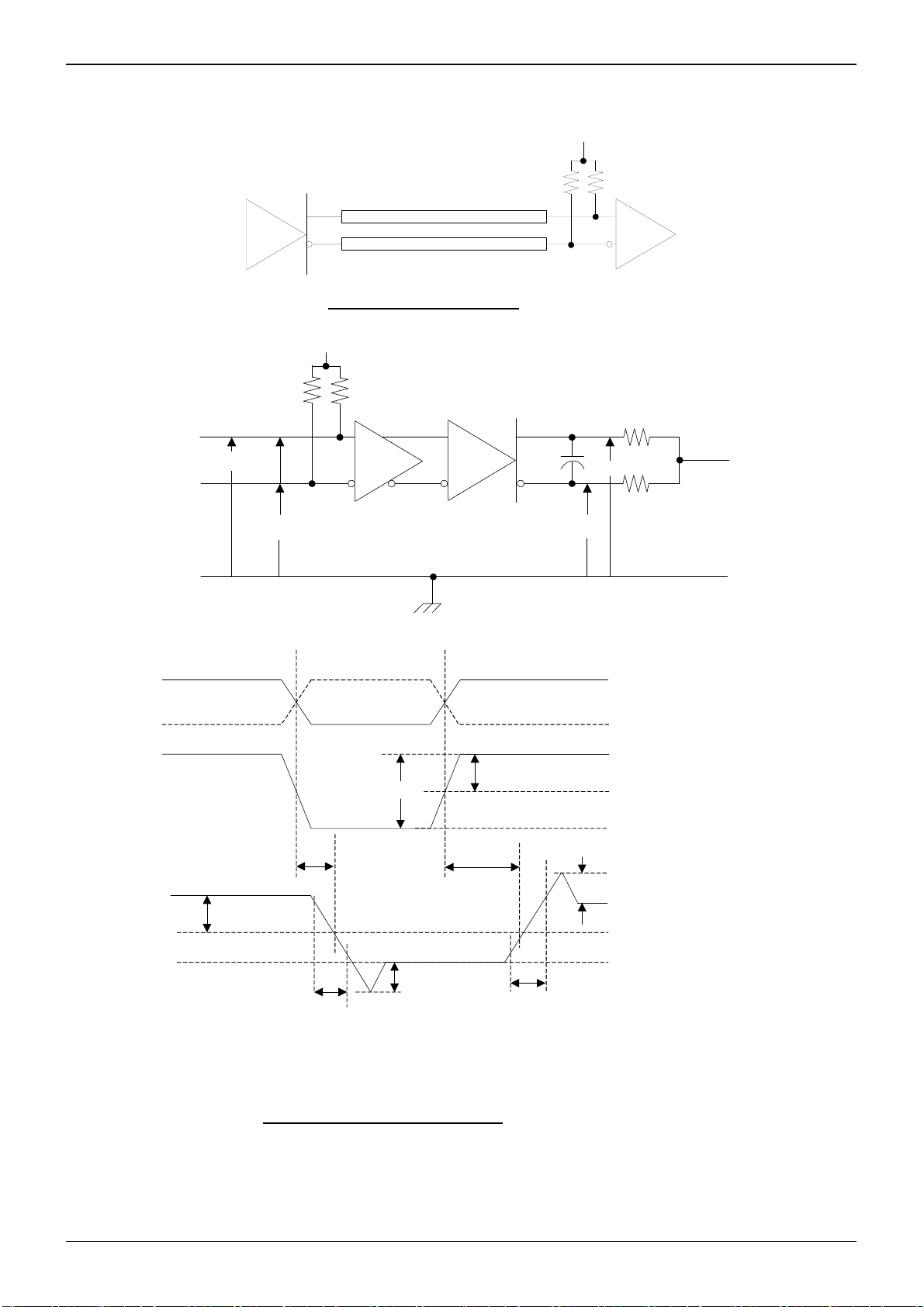
●Measurement Symbol And Circuit
Technical Note
AVcc
T
R
Receive
TMDS
TMDS
Drive
Zo = R
Zo = R
T
R
T
T
Figure 1 TMDS Output Driver
Vcc
RINT
VY
RT
RT
AVCC
Y
A
B
TMDS
Driver
TMDS
Receiver
Vswing = VY - VZVID = VA - VB
CL
0.5pF
Z
VZ
VA
RINT
VID
VB
VA
VB
Vcc V
Vcc-0.4 V
0.4 V
VIC
VID(pp)
0 V
-0.4 V
tPLH
80%
Vswing
tPLH
100%
VOD(O)
0V Differential
20%
tf
VOD(U)
tr
0%
Figure 2 Test Circuit and Definitions
www.rohm.com
6/19
© 2010 ROHM Co., Ltd. All rights reserved.
2010.05 - Rev.E

BU16006KV, BU16018KV, BU16024KV, BU16027KV
VY
VZ
tsk(D)
Figure 3 Definition of Intra-Pair Differential Skew
A
Port 1
B
A
Port 2
B
A
Port 3
B
S1
Clocking
S2
Output
tsx
Y
Z
tsx
75mV
-75mV
HI-Z
Technical Note
VOH
50%
VOL
Vcc V
Vcc-0.4 V
Vcc-0.4 V
Vcc V
Vcc-0.4 V
Vcc V
VDD
2
VDD
0V
75mV
-75mV
HPD_SINK
HPD1
HPD2
HPD3
S1
S2
SDA_SINK
80%
20%
tpdHLRT(DDC)
1.5V
tdis
Figure 4 TMDS Outputs Control Timing Definitions
tpdHL(HPD)
tpdLHRT(DDC)
tpdHLTR(DDC)
tpdLH(HPD)
tpdLHTR(DDC)
V
IL
ten
tsx(HPD)
t
(DDC)
SX
VDD
2
VDD
2
2.4V
0V
Vcc
2
VDD
SDA1
SDA2
SDA3
1.5V
tfTX(DDC) trTX(DDC) tfRX(DDC) trRX(DDC)
RX to TX TX to RX
80%
20%
0V
VDD
Figure 5 DDC and HPD Timing Definitions
www.rohm.com
7/19
© 2010 ROHM Co., Ltd. All rights reserved.
2010.05 - Rev.E

BU16006KV, BU16018KV, BU16024KV, BU16027KV
●Reference Data of BU16027KV/BU16006KV
Technical Note
Figure 6 Supply voltage(Vcc) vs. Supply current(Icc) of BU16006KV/BU16027KV [S1=H,S2=L]
www.rohm.com
8/19
© 2010 ROHM Co., Ltd. All rights reserved.
2010.05 - Rev.E

BU16006KV, BU16018KV, BU16024KV, BU16027KV
●Pin Assignment and Block Diagram of BU16006KV
Reserve2
HPD2
SDA2
SCL2
B21
A21
Vcc
B22
A22
GND
B23
A23
Vcc
B24
A24
A13
Vcc
A14
48
49
50
51
52
53
54
55
56
57
58
59
60
61
62
63
NC
64
B13
B14
46
44
45
47
BU16006KV
3
412
NC
NC
NC
GND
Vcc
A12
GND
B12
40
41
42
43
(64-pin VQFP)
NC
NC
NC
Vcc
98765
GND
A11
B11
SCL1
SDA1
HPD1
Reserve1
S2
A24
37
38
39
10
NC
34
33
36
35
32
S1
31
HPD_SINK
30
SDA_SINK
SCL_SINK
29
28
GND
27
Z1
Y1
26
25
Vcc
24
Z2
23
Y2
22
GND
21
Z3
20
Y3
19
Vcc
18
Z4
17
12
11
141316
15
NC
NC
NC
Vcc
GND
VSADJ
Y4
B24
A23
B23
A22
B22
A21
B21
HPD1
HPD2
SCL1
SDA1
SCL2
SDA2
●Pin Explanation List
Terminal
Name No.
I/O Description
A11, A12, A13, A14 39, 42, 45, 48 I Source port 1 TM DS positive inputs
A21, A22, A23, A24 54, 57, 60, 63 I Source port 2 TM DS positive inputs
B11, B12, B13, B14 38, 41, 44, 47 I Source port 1 TM DS negative inputs
B21, B22, B23, B24 53, 56, 59, 62 I Source port 2 TM DS negative inputs
GND
3, 9, 15, 22,
28, 43, 58
- Ground
HPD1 35 O Source port 1 hot plug detector output
HPD2 50 O Source port 2 hot plug detector output
HPD_SINK 31 I Sink port hot plug detector input
Reserve1 34 I/O Set to HIGH/LOW/OPEN
Reserve2 49 I/O Non Connect Pin
SCL1 37 I/O Source port 1 DDC I2C clock line
SCL2 52 I/O Source port 2 DDC I2C clock line
SCL_SINK 29 I/O Sink port DDC I2C clock line
SDA1 36 I/O Source port 1 DDC I2C data line
SDA2 51 I/O Source port 2 DDC I2C data line
SDA_SINK 30 I/O Sink port DDC I2C data line
S1, S2 32, 33 I Source selector
Vcc
6, 12, 19, 25,
40, 46, 55, 61
- Power supply
VSADJ 16 I T MDS compliant voltage swing control (4.64kΩ to GND)
Y1, Y2, Y3, Y4 26, 23, 20, 17 O TMDS positive outputs
Z1, Z2, Z3, Z4 27, 24, 21, 18 O TMDS negative outputs
Technical Note
A11
B11
TMD
R
S
X
V
CC
R
INTRINT
TMD
S
R
X
V
CC
R
INTRINT
TMD
S
R
X
V
CC
R
INTRINT
TMD
S
R
X
V
CC
R
INTRINT
TMD
S
R
X
B13
A14
B14
A13
A12
B12
R
R
R
V
V
INT
INT
CC
CC
R
R
INT
INT
TMD
R
R
S
X
X
R
V
V
INT
INT
CC
CC
R
R
INT
INT
TMD
TMD
R
S
S
X
Y4
TMDS
Drive
Z4
Y3
TMDS
Drive
Z3
Y2
TMDS
Drive
Z2
Y1
TMDS
Drive
Z1
VSADJ
S1
S2
HPD_SINK
Control Logic
SCL_SINK
SDA_SINK
www.rohm.com
9/19
© 2010 ROHM Co., Ltd. All rights reserved.
2010.05 - Rev.E

BU16006KV, BU16018KV, BU16024KV, BU16027KV
_
A11
B11
A12
●Pin Assignment and Block Diagram of BU16018KV
CC
B3457A3458GND59TEST3
CC
B3251A3252GND53B3354A3355V
CC
TEST241OE42V
HPD344SDA345SCL346GND47B3148A3149V
V
CC
HPD2 62
SDA2 63
SCL2 64
GND 65
GND
B21
A21
V
CC
B22
A22
GND
B23
A23
V
CC
B24
A24
GND
V
CC
HPD1
61
66
67
68
69
70
71
72
73
74
75
76
77
78
79
80
56
60
1
2
3
4
5
50
6
7
8
9
10
11
12
13
43
40 HPD_SINK
39 SDA_SINK
38 SCL_SINK
37 GND
36 GND
35 Z1
34 Y1
33 V
32 Z2
31 Y2
30
29
28
27
26
25
24
23 S3
22 S2
14
15 16
21 S1
17
18
19
20
GND
Z3
Y3
V
Z4
Y4
GND
CC
CC
TEST0
SDA1
CC
V
A11
B11
B12
GND
SCL1
CC
CC
V
A12
A13
B13
GND
V
A14
B14
PRE
GND
TEST1
VSADJ
A24
B24
A23
B23
A22
B22
A21
B21
A34
B34
A33
B33
A32
B32
A31
B31
HPD1
HPD2
HPD3
SCL1
SDA1
SCL2
SDA2
SCL3
SDA3
V
CC
R
INTRINT
TMD
S
R
X
V
CC
R
INTRINT
TMD
S
R
X
V
CC
R
INTRINT
TMD
S
R
X
V
CC
R
INTRINT
TMD
S
R
X
V
CC
R
INTRINT
TMD
S
R
X
V
CC
R
INTRINT
TMD
S
R
X
V
CC
R
INTRINT
TMD
S
R
X
V
CC
R
INTRINT
TMD
S
R
X
B12
R
R
V
INT
INT
CC
R
R
INT
INT
TMD
TMD
R
R
S
S
X
X
B13
A13
R
V
INT
CC
R
INT
TMD
R
S
X
Technical Note
A14
B14
R
V
V
INT
CC
CC
R
INT
TMD
R
S
X
3-to-1 MUX
Control Logic
●Pin Explanation List
Terminal
Name No.
I/O Description
A1 1, A12, A13, A14 6, 9, 12, 15 I Port 1 TMDS positive inputs
A21, A22, A23, A24 68, 71, 74, 77 I Port 2 TMDS positive inputs
A31, A32, A33, A34 49, 52, 55, 58 I Port 3 TMDS positive inputs
B11, B12, B13, B14 5, 8, 11, 14 I Port 1 TMDS negative inputs
B21, B22, B23, B24 67, 70, 73, 76 I Port 2 TMDS negative inputs
B31, B32, B33, B34 48, 51, 54, 57 I Port 3 TMDS negative inputs
GND
4, 10, 16, 24, 30, 36, 37, 47,
53, 59, 65, 66, 72, 78
- Ground
HPD1 80 O Port 1 hot plug detector output
HPD2 62 O Port 2 hot plug detector output
HPD3 44 O Port 3 hot plug detector output
HPD_SINK 40 I Sink side hot plug detector input
TEST0,1,2,3
______
OE
42 I Output enable, active low
PRE 19 I
1, 20, 41, 60 Open or GND connect (recommend)
TMDS high speed mode SW High : ON, Low : OFF
(above 165MHz recommend to High)
SCL1 3 I/O Source port 1 DDC I2C clock line
SCL2 64 I/O Source port 2 DDC I2C clock line
SCL3 46 I/O Source port 3 DDC I2C clock line
SCL_SINK 38 I/O
Sink port DDC I2C clock line
SDA1 2 I/O Source port 1 DDC I2C data line
SDA2 63 I/O Source port 2 DDC I2C data line
SDA3 45 I/O Source port 3 DDC I2C data line
SDA_SINK 39 I/O Sink port DDC I2C data line
S1, S2, S3 21, 22, 23 I Source selector input
VCC
7, 13, 17, 27, 33, 43, 50, 56,
61, 69, 75, 79
- Power supply
VSADJ 18 I TMDS voltage swing control. Connect to GND 4.64KΩ
Y1, Y2, Y3, Y4 34, 31, 28, 25 O TMDS positive outputs
Z1, Z2, Z3, Z4 35, 32, 29, 26 O TMDS negative outputs
PRE
VSADJ
Y4
TMDS
Drive
Z4
Y3
TMDS
Drive
Z3
Y2
TMDS
Drive
Z2
Y1
TMDS
Drive
Z1
OE
S1
S2
S3
HPD_SINK
SCL_SINK
SDA_SINK
www.rohm.com
10/19
© 2010 ROHM Co., Ltd. All rights reserved.
2010.05 - Rev.E

BU16006KV, BU16018KV, BU16024KV, BU16027KV
Technical Note
●Pin Assignment and Block Diagram of BU16024KV
TEST3
TEST2
GND
SCL_SINK
SDA_SINK
Vcc
SELREF
GND
Vcc
SDA
SCL
VSADJ
36
35
HPD
GND
B11
A11
Vcc
B12
A12
GND
B13
A13
Vcc
NC
37
38
39
40
41
42
43
44
45
46
47
48
343332313029282726
16024KV
(48-pin VQFP)
123456789
101112
25
24
HPD_SINK
23
GND
22
Z1
21
Y1
20
Vcc
19
Z2
18
Y2
17
GND
16
Z3
15
Y3
14
Vcc
13
NC
TEST0
Vcc
A14
B14
GND
OEB
I2CEN
PRE
GND
Z4
Y4
TEST1
VSADJ
OE
PRE
V
CC
R
INT
A4
B4
A3
B3
A2
B2
A1
B1
SCL
SDA SDA_SINK
I2CEN
SELREF
TMDS
Rx
V
CC
R
INT
TMDS
Rx
V
CC
R
INT
TMDS
Rx
V
CC
R
INT
TMDS
Rx
HPD
(*) when HPD_SINK = “L”. Termination resistor is turned off.
●Pin Explanation List
Terminal
Name No.
I/O Description
B1, B2, B3, B4 39, 42, 45, 2 I TMDS Negative inputs
A1, A2, A3, A4 40, 43, 46, 3 I TMDS Positive inputs
Z1, Z2, Z3, Z4 22, 19, 16, 11 O TMDS Negative outputs
Y1, Y2, Y3, Y4 21, 18, 15, 10 O TMDS Positive outputs
HPD 37 O Source side hot plug detector output
HPD_SINK 24 I Sink side hot plug detector input
SCL 34 I/O Source port DDC I2C clock line
SDA 33 I/O Source port DDC I2C data line
SCL_SINK 27 I/O Sink port DDC I2C clock line
SDA_SINK 28 I/O Sink port DDC I2C data line
VSADJ 35 I T M DS voltage swing control(4.64kΩ to GND)
I2CEN 6 I I2C Repeater enable Low : High-Z High : Active
SELREF 30 I SCL_SINK/SDA_SINK Output voltage select
TEST0, 1, 2, 3 1, 12, 25, 36 I Open or GND connect (recommend)
N.C 13, 48 Open or GND connect (recommend)
OEB 7 I
PRE 8 I
V
CC
GND
5, 14, 20, 29,
32, 41, 47
4, 9, 17, 23,
26, 31, 38, 44
TMDS Output enable
Low : Active High : High-Z
TMDS high speed mode SW High : ON, Low : OFF
(above 165MHz recommend to High)
- Power supply
- Ground
TMDS
Driver
TMDS
Driver
TMDS
Driver
TMDS
Driver
Y4
Z4
Y3
Z3
Y2
Z2
Y1
Z1
SCL_SINK
HPD_SINK(* )
www.rohm.com
11/19
© 2010 ROHM Co., Ltd. All rights reserved.
2010.05 - Rev.E

BU16006KV, BU16018KV, BU16024KV, BU16027KV
●Pin Assignment and Block Diagram of BU16027KV
A13
Vcc
A14
B13
B14
Vcc
A12
GND
B12
A11
B11
SCL1
SDA1
HPD1
S2
Reserve1
Reserve2
HPD2
SDA2
SCL2
B21
A21
Vcc
B22
A22
GND
B23
A23
Vcc
B24
A24
HPD3
1PIN
MARK
46
43
44
45
48
47
49
50
51
52
53
54
55
56
57
58
59
60
61
62
63
64
BU16027KV
BU16028KV
(64-pin VQFP)
3
412
A31
B31
GND
SCL3
SDA3
42
98765
10
Vcc
A32
B33
B32
GND
34
33
36
35
32
S1
31
HPD_SINK
30
SDA_SINK
29
SCL_SINK
28
GND
27
Z1
Y1
26
25
Vcc
24
Z2
23
Y2
22
GND
21
Z3
20
Y3
19
Vcc
18
Z4
17
12
11
141316
15
Vcc
A33
A34
B34
GND
VSADJ
Y4
37
38
394041
A24
B24
A23
B23
A22
B22
A21
B21
A34
B34
A33
B33
A32
B32
A31
B31
HPD1
HPD2
HPD3
SCL1
SDA1
SCL2
SDA2
SCL3
SDA3
V
CC
V
CC
V
CC
V
CC
V
CC
V
CC
V
CC
V
CC
A11
B11
TMD
R
S
X
R
INTRINT
TMD
S
R
X
R
INTRINT
TMD
S
R
X
R
INTRINT
TMD
S
R
X
R
INTRINT
TMD
S
R
X
R
INTRINT
TMD
S
R
X
R
INTRINT
TMD
S
R
X
R
INTRINT
TMD
S
R
X
R
INTRINT
TMD
S
R
X
B13
A12
B12
R
R
V
V
INT
INT
CC
CC
R
R
INT
INT
TMD
R
R
S
S
X
X
●Pin Explanation List
Name
Terminal
No.
I/O Description
A11, A12, A13, A14 39, 42, 45, 48 I Source port 1 TMDS positive inputs
A21, A22, A23, A24 54, 57, 60, 63 I Source port 2 TMDS positive inputs
A31, A32, A33, A34 5, 8, 11, 14 I Source port 3 TMDS positive inputs
B11, B12, B13, B14 38, 41, 44, 47 I Source port 1 TMDS negative inputs
B21, B22, B23, B24 53, 56, 59, 62 I Source port 2 TMDS negative inputs
B31, B32, B33, B34 4, 7, 10, 13 I Source port 3 TMDS negative inputs
GND 3, 9, 15, 22, 28, 43, 58 - Ground
HPD1 35 O Source port 1 hot plug detect or output (statu s pin)
HPD2 50 O Source port 2 hot plug detect or output (statu s pin)
HPD3 64 O Source port 3 hot plug detect or output (statu s pin)
HPD_SINK 31 I Sink port hot plug detector input (status pin)
Reserve1 34 I/O In High, Low, and Open, any setting is OK.
Reserve2 49 I/O Non Connect Pin
SCL1 37 I/O Source port 1 DDC I2C clock line
SCL2 52 I/O Source port 2 DDC I2C clock line
SCL3 2 I/O Source port 3 DDC I2C clock line
SCL_SINK 29 I/O Sink port DDC I2C clock line
SDA1 36 I/O Source port 1 DDC I2C data line
SDA2 51 I/O Source port 2 DDC I2C data line
SDA3 1 I/O Source port 3 DDC I2C data line
SDA_SINK 30 I/O Sink port DDC I2C data line
S1, S2 32, 33 I Source selector
Vcc
6, 12, 19, 25, 40, 46, 55,
61
- Power supply
VSADJ 16 I TMDS voltage swing control (via 4.64kΩ to GND)
Y1, Y2, Y3, Y4 26, 23, 20, 17 O Sink port TMDS positive outputs
Z1, Z2, Z3, Z4 27, 24, 21, 18 O Sink port TMDS negative outputs
A13
TMD
Technical Note
A14
B14
R
R
V
V
INT
INT
CC
CC
R
R
INT
INT
TMD
R
S
X
Y4
TMDS
Drive
Z4
Y3
TMDS
Drive
Z3
Y2
TMDS
Drive
Z2
Y1
TMDS
Drive
Z1
VSADJ
S1
S2
HPD_SINK
Control Logic
SCL_SINK
SDA_SINK
www.rohm.com
12/19
© 2010 ROHM Co., Ltd. All rights reserved.
2010.05 - Rev.E

BU16006KV, BU16018KV, BU16024KV, BU16027KV
/
●Source Selection Lookup Table of BU16006KV
Control Pins I/O Selected Output Status
HPD_SINK S1 S2 Y/Z
A1/B1
H H H
H L H
H L L
H H L
L H H
L L H
L L L
L H L
●Source Selection Lookup Table of BU16027KV
Control Pins I/O Selected Output Status
HPD_SINK S1 S2 Y/Z
H/L H H
H/L L H
H/L L L
H/L H L
●Source Selection Lookup Table of BU16018KV
Control Pins I/O Selected Output Status
HPD_SINK S1 S2 S3 Y/Z SCL_SINK/SDA_SINK HPD1 HPD2 HPD3
H H X X
H L H X
H L L H
H L L L
L H X X
L L H X
L L L H
L L L L
H: Logic high; L: Logic low; X: Don’t care; Z: High impedance
Termination resistors of A2/B2 and A3/B3
are disconnected
A2
Termination resistors of A1/B1 and A3/B3
are disconnected
Disallowed (indeterminate) State
All termination resistors are disconnected
All termination resistors are disconnected
Disallowed (indeterminate) State
All termination resistors are disconnected
Disallowed (indeterminate) State
All termination resistors are disconnected
Disallowed (indeterminate)State
All termination resistors are disconnected
All termination resistors are disconnected
Termination resistors of A2/B2
and A3/B3 are disconnected
Termination resistors of A1/B1
and A3/B3 are disconnected
Termination resistors A1/B1 and
A2/B2 are disconnected
None (Z)
All terminations are disconnected
Termination resistors of A2/B2
and A3/B3 are disconnected
Termination resistors of A1/B1
and A3/B3 are disconnected
Termination resistors of A1/B1
and A2/B2 are disconnected
All terminations are disconnected
Disallowed (indeterminate)State
All terminations are disconnected
Disallowed (indeterminate)State
All terminations are disconnected
Disallowed (indeterminate)State
All terminations are disconnected
All terminations are disconnected
B2
None (Z)
None (Z)
A1/B1
A2/B2
A3/B3
A1/B1
A2/B2
A3/B3
None (Z)
None (Z)
SCL_SINK
SDA_SINK
SCL1
SDA1
SCL2
SDA2
None (Z)
SCL1
SDA1
SCL2
SDA2
None (Z)
SCL_SINK
SDA_SINK
SCL1
SDA1
SCL2
SDA2
SCL3
SDA3
None (Z)
None (Z) H H H
None (Z) L L L
HPD1 HPD2 HPD3
HPD
_SINK
L
L L
HPD
_SINK
SCL1
SDA1
SCL2
SDA2
SCL3
SDA3
SCL1
SDA1
SCL2
SDA2
SCL3
SDA3
Technical Note
HPD1 HPD2 HPD3
H L L
L H L
L L H
H H H
L L L
L L L
L L L
L L L
L L
HPD
_SINK
HPD
_SINK
H L L
L H L
L L H
L L L
L L L
L L L
L
HPD
_SINK
HPD
_SINK
www.rohm.com
13/19
© 2010 ROHM Co., Ltd. All rights reserved.
2010.05 - Rev.E

BU16006KV, BU16018KV, BU16024KV, BU16027KV
●Equivalent Input And Output Schematic Diagrams
Technical Note
Anm
SCL_SINK
SDA_SINK
SCL
SDA
50Ω
R-Side I
TMDS Input Stage
V
DD
2
C Input/Output Stage
V
DD
50Ω
Bnm
TMDS Output Stage
V
DD
10mA
T-Side I2C Input/Output Stage
HPD_SINK
※n=1,2,3 m=1,2,3,4
HPD Output Stage
V
DD
V
DD
Ym
Zm
HPDn
V
DD
V
DD
www.rohm.com
14/19
© 2010 ROHM Co., Ltd. All rights reserved.
2010.05 - Rev.E

BU16006KV, BU16018KV, BU16024KV, BU16027KV
●Note for use
1). Attention on use as “repeater” or “source” equipment.
Y and Z terminals are connected to Vcc through ESD diode as Figure 7. When Vcc+0.4 < AVcc, leak current flows from
AVcc to Vcc. For this current, BU16006KV/BU16027KV can’t pass the compliance test as “Repeater” and “Source”
equipment (Test ID 7-3 VOFF). BU16018KV/BU16024KV is able to pass the compliance test using external element lik e
Figure 8
Vcc=0V
Vcc=0V
Ym
Voff
50
AVcc=3.3V
Technical Note
Ioff
50
Ioff
Zm
AVcc=3.3V
Voff
Figure 7 TMDS Equivalent output schematic
Figure 8 Leak current control in BU16018KV an d BU16024KV
www.rohm.com
15/19
© 2010 ROHM Co., Ltd. All rights reserved.
2010.05 - Rev.E

BU16006KV, BU16018KV, BU16024KV, BU16027KV
Technical Note
2). HPD_SINK Pull down resistance.
HPD_SINK have a 5V tolerant structure shown in Figure 9.It needs some drive current to pull down HPD_SINK "H" to "L".
So to pull down HPD_SINK, please use 10kΩ(or under 10kΩ) resistor.
Figure 9 HPD_SINK I/O schematic
3). About don’t use terminal.
3-1. Unused TMDS input channel recommend open.
Vcc
R
INT
A
B
R
INT
TMDS
Receiver
TMDS
Driver
Figure 10 TMDS Input Recommendation
3-2. Unused DDC Buffers of R side recommend to pull up to Vcc.
Vcc
BU160**KV
Y
Z
R
T
AVcc
R
T
4.7k
SCL
SDA
T
SCL_SINK
SDA_SINK
R
Figure 11 Unused DDC Buffers of R side
www.rohm.com
16/19
© 2010 ROHM Co., Ltd. All rights reserved.
2010.05 - Rev.E

BU16006KV, BU16018KV, BU16024KV, BU16027KV
A
A
3-3. Unused DDC Buffers of R side recommend pull up to Vcc.
Vcc
Technical Note
4.7k
RSCL
RSD
T
TSCL
TSD
R
Figure 12 Unused DDC of T side
3-4. Unused HPDn recommend open.
Figure 13 Open unused HPDn
4). About serial connection notice.
When BU160xxKV output connect to other HDMI sw input like following application the specification of Jitter toleranc e is
downed. Especially when system needs 1080p (12bit) data rate and cable or PCB trace lengths bet ween BU160xxKV i nput
and output is small, Deteriorations of Jitter tolerance is outstanding. This problem also depends on receiver IC
characteristic. When system is required 1080p (12bit), Rohm doesn’t recommend serial connect application.
Figure 14 serial connection notice
www.rohm.com
17/19
© 2010 ROHM Co., Ltd. All rights reserved.
2010.05 - Rev.E

BU16006KV, BU16018KV, BU16024KV, BU16027KV
5). AC Coupling notice
BU160xxKV can also communicate using AC coupling capacitor with TMDS line. But even connecting AC coupling
capacitor, AC current may flow if input common mode voltage between two devices is different. For this current, the lower
common mode voltage devices like PCIe or DP may be damaged by AC current.
Technical Note
Figure 15 AC Coupling connection notice
6). TMDS output offset voltage notice.
Offset voltage may appear to TMDS output when there is no signal to TMDS input differential line. OE should set to “H” to
avoid it.
7). Limitation of Master and slave direction as shown Figure 16.
Figure 16 Limitation of Master and slave direction
www.rohm.com
18/19
© 2010 ROHM Co., Ltd. All rights reserved.
2010.05 - Rev.E

BU16006KV, BU16018KV, BU16024KV, BU16027KV
●Ordering part number
B U 1 6 0 0 6 K V - E 2
Part No. Part No.
16006
16018
16024
16027
VQFP80
60
14.0± 0.2
12.0± 0.1
41
4061
12.0± 0.1
14.0± 0.2
1.6MAX
1.4± 0.05
1.25
80
0.1±0.05
1
0.5± 0.1
1PIN MARK
+0.05
0.2
-
0.04
1.25
21
20
0.145
+6
4
–4
0.08 S
M
0.08
+0.05
-
0.03
0.5± 0.15
1.0± 0.2
S
(Unit : mm)
VQFP64
12.0±0.2
10.0±0.1
12.0±0.2
1.6MAX
10.0±0.1
1.4±0.05
1.25
48
49
64
1
0.1±0.05
1PIN MARK
0.5±0.1
33
32
1.25
17
16
+6
4
–4
0.08
S
+0.05
0.2
-
0.04
0.08
M
0.145
0.5±0.15
+0.05
-
0.03
1.0±0.2
(Unit : mm)
Package
KV: VQFP80
(BU16018),
VQFP64
(BU16027 /
BU16006),
VQFP48C
(BU16024)
<Tape and Reel information>
Embossed carrier tape (with dry pack)Tape
Quantity
Direction
of feed
<Tape and Reel information>
Quantity
Direction
of feed
1000pcs
E2
The direction is the 1pin of product is at the upper left when you hold
()
reel on the left hand and you pull out the tape on the right hand
1pin
Reel
Embossed carrier tape (with dry pack)Tape
1000pcs
E2
The direction is the 1pin of product is at the upper left when you hold
()
reel on the left hand and you pull out the tape on the right hand
1pin
Reel
Packaging and forming specification
E2: Embossed tape and reel
Direction of feed
Order quantity needs to be multiple of the minimum quantity.
∗
Direction of feed
Order quantity needs to be multiple of the minimum quantity.
∗
Technical Note
VQFP48C
9.0± 0.2
7.0± 0.1
25
121
1PIN MARK
0.22
+0.05
-
0.04
24
13
0.08 S
0.75
0.145
0.08
+0.05
-
0.03
4
M
1.0±0.2
0.5±0.15
+6
–4
9.0± 0.2
1.6MAX
1.4± 0.05
36
37
7.0± 0.1
48
0.75
0.5± 0.1
0.1± 0.05
(Unit : mm)
www.rohm.com
19/19
© 2010 ROHM Co., Ltd. All rights reserved.
<Tape and Reel information>
Embossed carrier tapeTape
Quantity
Direction
of feed
1500pcs
E2
The direction is the 1pin of product is at the upper left when you hold
()
reel on the left hand and you pull out the tape on the right hand
1pin
Reel
Direction of feed
Order quantity needs to be multiple of the minimum quantity.
∗
2010.05 - Rev.E

Notes
No copying or reproduction of this document, in part or in whole, is permitted without the
consent of ROHM Co.,Ltd.
The content specied herein is subject to change for improvement without notice.
The content specied herein is for the purpose of introducing ROHM's products (hereinafter
"Products"). If you wish to use any such Product, please be sure to refer to the specications,
which can be obtained from ROHM upon request.
Examples of application circuits, circuit constants and any other information contained herein
illustrate the standard usage and operations of the Products. The peripheral conditions must
be taken into account when designing circuits for mass production.
Great care was taken in ensuring the accuracy of the information specied in this document.
However, should you incur any damage arising from any inaccuracy or misprint of such
information, ROHM shall bear no responsibility for such damage.
The technical information specied herein is intended only to show the typical functions of and
examples of application circuits for the Products. ROHM does not grant you, explicitly or
implicitly, any license to use or exercise intellectual property or other rights held by ROHM and
other parties. ROHM shall bear no responsibility whatsoever for any dispute arising from the
use of such technical information.
Notice
The Products specied in this document are intended to be used with general-use electronic
equipment or devices (such as audio visual equipment, ofce-automation equipment, communication devices, electronic appliances and amusement devices).
The Products specied in this document are not designed to be radiation tolerant.
While ROHM always makes effor ts to enhance the quality and reliability of its Products, a
Product may fail or malfunction for a variety of reasons.
Please be sure to implement in your equipment using the Products safety measures to guard
against the possibility of physical injury, re or any other damage caused in the event of the
failure of any Product, such as derating, redundancy, re control and fail-safe designs. ROHM
shall bear no responsibility whatsoever for your use of any Product outside of the prescribed
scope or not in accordance with the instruction manual.
The Products are not designed or manufactured to be used with any equipment, device or
system which requires an extremely high level of reliability the failure or malfunction of which
may result in a direct threat to human life or create a risk of human injury (such as a medical
instrument, transportation equipment, aerospace machinery, nuclear-reactor controller, fuelcontroller or other safety device). ROHM shall bear no responsibility in any way for use of any
of the Products for the above special purposes. If a Product is intended to be used for any
such special purpose, please contact a ROHM sales representative before purchasing.
If you intend to export or ship overseas any Product or technology specied herein that may
be controlled under the Foreign Exchange and the Foreign Trade Law, you will be required to
obtain a license or permit under the Law.
Thank you for your accessing to ROHM product informations.
More detail product informations and catalogs are available, please contact us.
ROHM Customer Support System
www.rohm.com
© 2010 ROHM Co., Ltd. All rights reserved.
http://www.rohm.com/contact/
R1010
A
 Loading...