

Page 1

PWM Power Unit
)
)
(
)
(
)
j
g
The device allows continuous power control for lamps,LEDs or
inductive loads.
•
Highside switch
•
Overtemperatur protection
•
Short circuit / overload protection through pulse width
reduction and overload shutdown
•
Load dump protection
•
Undervoltage and overvoltage shutdown with auto-restart and hysteresis
•
Reverse battery protection
•
Timing frequency adjustable
•
Controlled switching rise and fall times
•
Maximum current internally limited
•
Protection against loss of GND
•
Electrostatic discharge (ESD) protection
•
Package: P-DSO-20-6 (SMD)
1)
2)
BTS 730
Note:
Switching frequency is programmed with an external capacitor.
Type Ordering Code Marking Package
BTS730 Q67060-S7007-A2 - P-DSO-20-6
Maximum Ratings
Parameter Symbol Values Unit
Active overvoltage prodection
Short circuit current
Input current (DC
Pin1
C
and pin19
t
V
C
Operating temperature range
Storage temperature range
3)
Power dissipation
T
=25°C
a
T
=85°C 2 W
a
Thermal resistance chip-case
chip-ambient
3)
V
bb (AZ
I
SC
I
Ct
I
VC
T
T
st
P
tot
R
th JC
R
th JA
>40 V
self-limited 2 mA
2 mA
-40...+150 °C
-50...+150
3 W
≤
≤
35
75
K/W
1)
With 150Ω resistor in signal GND connection.
2)
Potential between signal GND and load GND >0.5V
3)
Device on 50mm*50mm*1.5mm epoxy PCB FR4 with 6 cm2(one layer,70µm thick) copper area for V
conection, PCB is vertical without air blowing.
bb
Semiconductor Group 1 12.96
Page 2
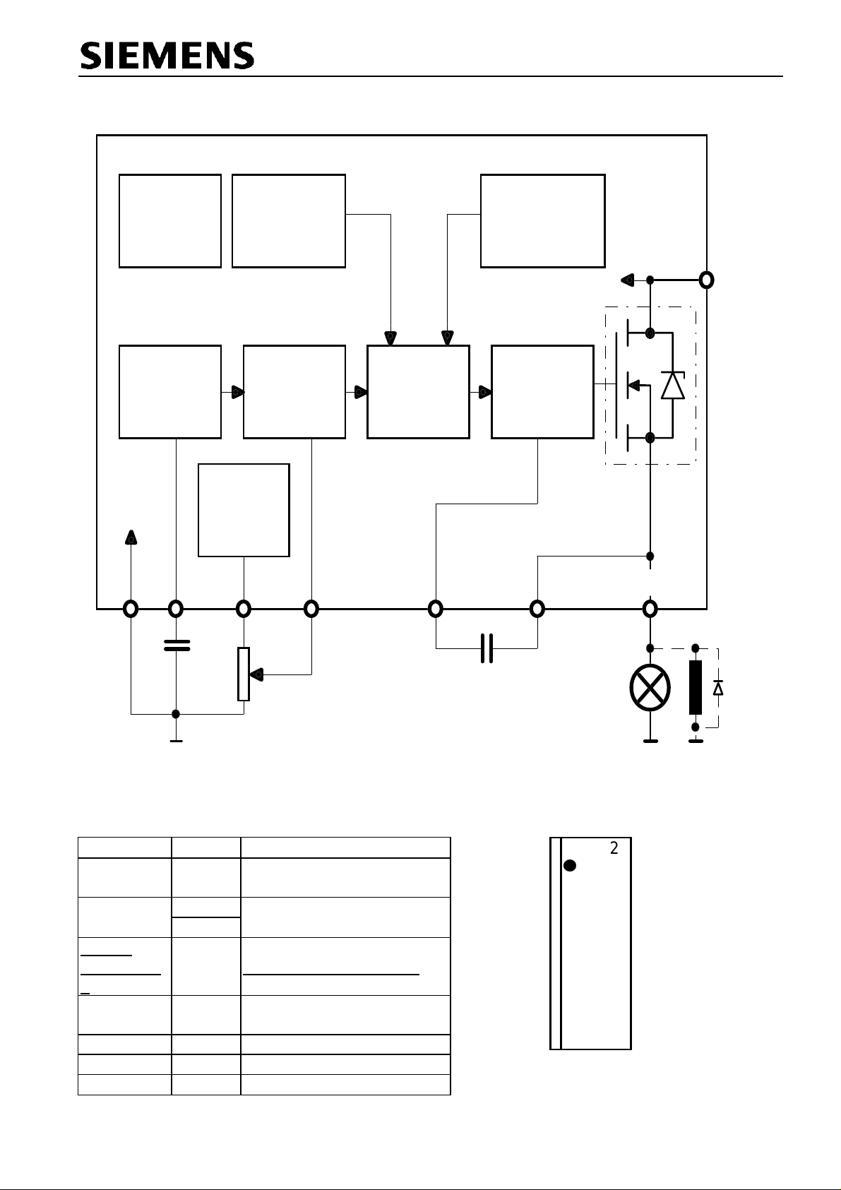
Block Diagram
y
(
)
g
Overvoltage
Prodtection
Over / Undervoltage
Detection
Temperature
Sensor
(4,5,6,7)
(14,15,16,17)
BTS 730
V
bb
(18)
GND
Timing
Generator
Pulse - width
Comparator
Logic
Current
Limiting
Voltage
Regulator
Pump and
(1) (20) (19) (2)
t REF
VVC
C
C
B1
(3)
(8,9,10,11,12,13)
C
B2
Timing
Cap.
25k68nF
Bootstrap
Capacitor
22nF
nal GND Load GND
Si
OUT
V
V
V
V
V
V
REF
C
bb
bb
bb
bb
(top view)
Pin Definitions and Funktions
Pin Symbol Funktions
1
2
3
4,5,6,7
14,15,16,1
7
8,9,10 OUT Output
11,12,13
18 GND Ground
19
20
Semiconductor Group 2
C
t
Timing capacitor
for frequenc
C
C
V
B1
B2
bb
Bootstrap capacitor
Supply voltage
Leadframe connected
V
V
C
REF
Voltage for PWM-Control
Reference Voltage
Pin Configuration
C
t
1
%
C
C
V
V
V
V
B1
B2
bb
bb
bb
bb
2 19
3 18 GND
4 17
5 16
6 15
7 14
OUT 8 13 OUT
OUT 9 12 OUT
OUT 10 11OUT
20
Page 3

BTS 730
1)
2)
)
)
(on)
(
)
j
Electrical Characteristics
T
at
j
Parameter Symbol Values Unit
On-state resistance
I
=3A,
L
Operating voltage
T
= -40 ...+150iC
j
Nominal current,
calculated value
ISO-standard:
Vbb-V
Load current limit
V
-
V
bb
Undervoltage shutdown
I
= 3A
L
Overvoltage shutdown
I
= 3A
L
Max.output voltage (RMS)
I
= 3A,
L
Reference voltage
= 10mA
I
REF
Reference current
pin 18 (GND) to pin 20 (V
Internal current
consumption during
operation, measured in PWM gap
Bootstrap voltage, pin 2
(
C
B1
= 12 V,
V
bb
PWM frequency
= -40 ... +150 °C,
T
c
Max. pulse duty factor
= 3A,
I
L
Min. pulse duty factor
= 3A,
I
L
Slew rate "on" du/d
10 ... 90%
Slew rate "off" du/d
90 ... 10%
Thermal overload trip
temperature
1)
Note:
2)
Note:
i
= 25
) to pin 3 (
C, unless otherwise specified.C
V
=12V
bb
≤ 0.5V, Tc=85°C
OUT
> 1V
OUT
> 12 V
V
bb
)
C
B2
=0V , (50%
V
C
=0V , (50%
V
C
I
OUT
I
OUT
undervoltage shutdown
overvoltage shutdown
REF
= 68 nF
C
t
V
OUT
V
OUT
Bootstrap
= 22nF
min. typ. max.
R
ON
V
bb
I
-ISO 3 - - A
L
I
LLim
V
bb(LOW
V
bb(HI
V
RMSmax
V
REF
I
REF
5.9
3 4.2 5.4 V
17 18 19 V
12 - 14 V
2 3 V
- - 70
16.9
- 20 - A
- 150 - mA
) short
I
R
V
B
f
PWM
D
imax
50 - 100 Hz
95 98 - %
- 5 mA
- 10 - V
)
D
imin
- 8 14 %
)
t
t
off
T
20 - 120
20 - 120
150 - - °C
mΩ
V
mV/µs
mV/µs
Semiconductor Group 3
Page 4
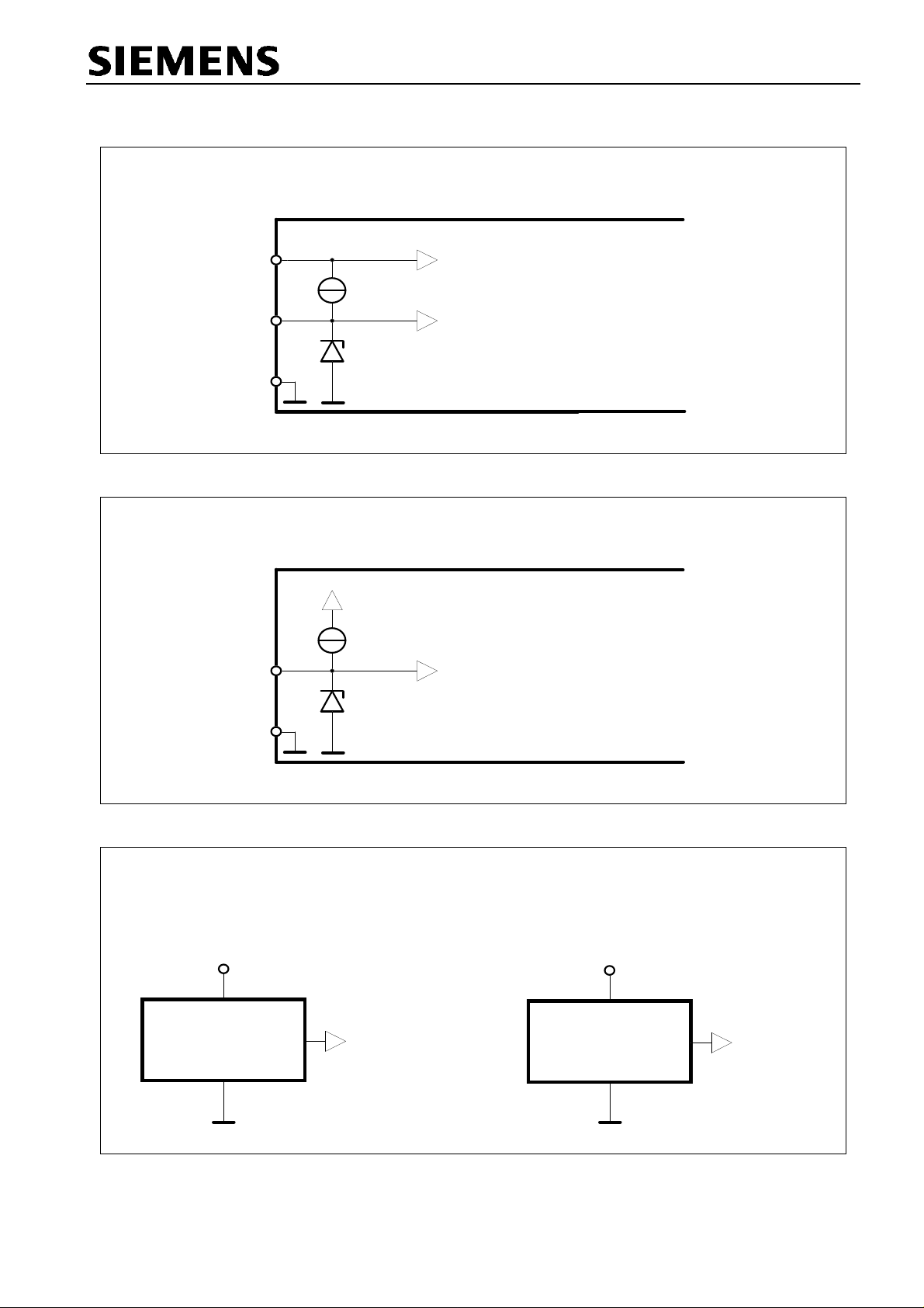
Circuits
BTS 730
Analog Logic-Input
V
REF
V
C
GND
(20)
(19)
(18)
V
Triangular Waveform
(19)
C
Voltage Regulator
µ
2
A
Pulse-width Comparator
6V
max. 2mA
Generator Input
V
bb
C
(1)
t
µ
6
A
C
t
(1)
Timing Generator
6V
GND
(18)
max. 2mA
Voltage Sensor (typ)
Undervoltage Sensor Overvoltage Sensor
V
+V
< 4.2 V
bb
bb
Signal to the
logic unit
V
+V
bb
bb
> 18 V
Signal to the
logic unit
GND
Semiconductor Group 4
GND
Page 5
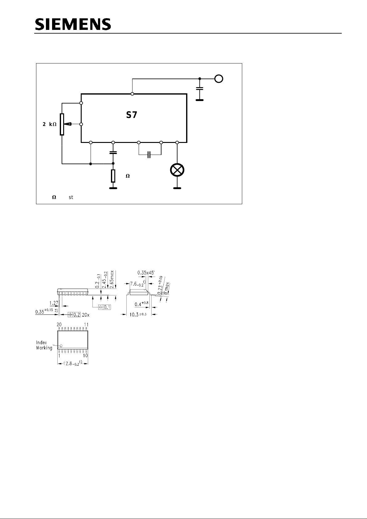
Application Note
Dimming of dashboard lighting
4,5,6,7
14,15,16,17
220nF
BTS 730
+
V
bb
20
V
REF
k25
O
O
19
V
C
GND
150
O
Resistor for reverse battery and load dump prodection
O
Package Outline
18
V
bb
BTS730
68nF
O
O
C
C
t
123
150
P-DSO-20-6
B1
22nF
C
OUT
B2
8,9,10
11,12,13
Load
Dimensions in mm
Semiconductor Group 5
Page 6
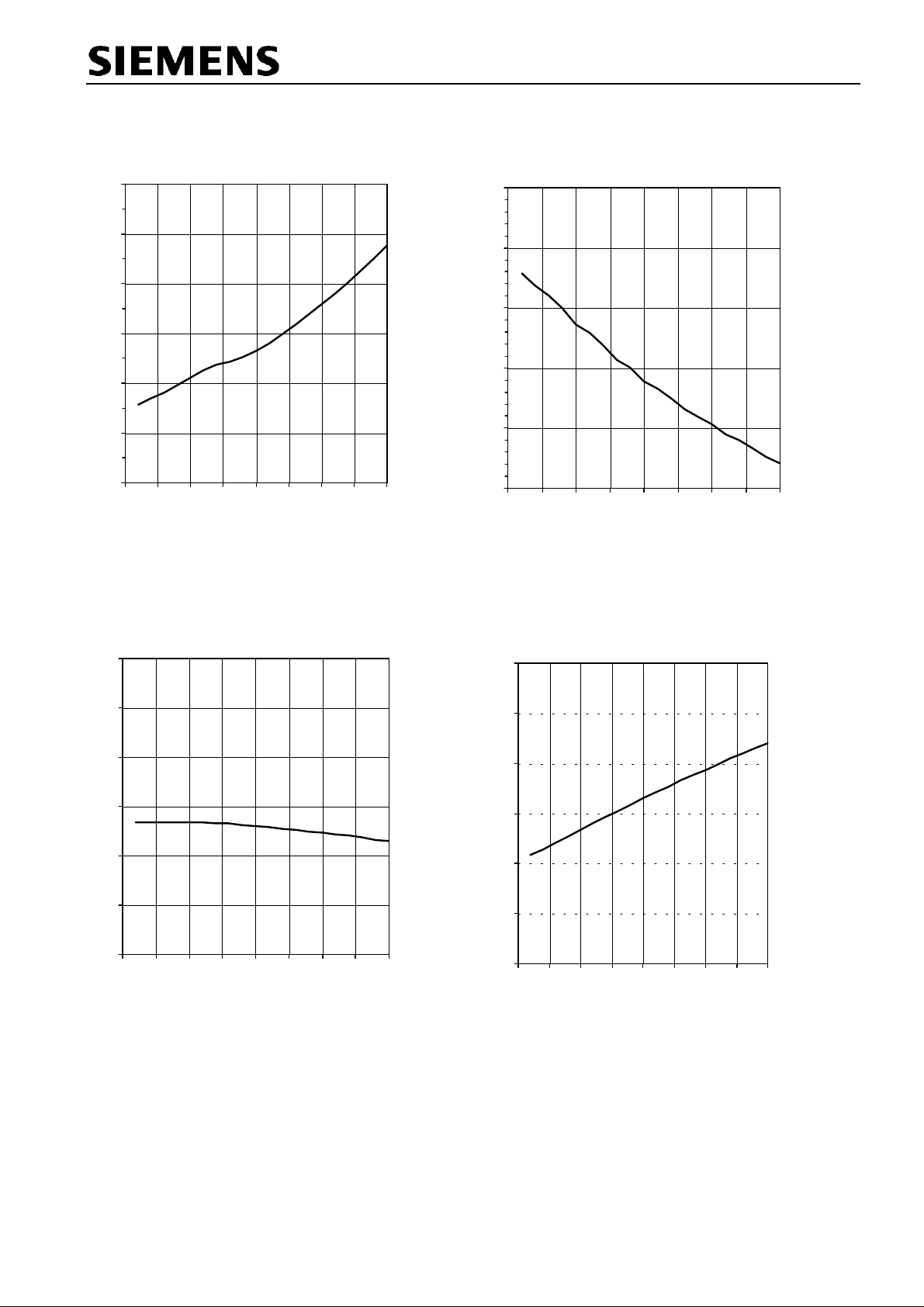
BTS 730
Typ.on-state resistance
Ω
m
140
120
100
80
60
40
20
-50 -25 0 25 50 75 100 125 150
R
ON
= f(
T
)
C
TC °C
Typ. Load current limit
I
A
30
25
20
15
10
5
-50 - 25 0 25 50 75 100 125 150
LLim
= f(
T
)
C
TC °C
Typ. undervoltage shutdow n
V
V
6,0
5,5
5,0
4,5
4,0
3,5
3,0
-50 -25 0 25 50 75 100 125 150
bb(LOW)
= f(
T
)
C
TC °C
Typ. overvoltage shut dow n
V
V
20,0
19,5
19,0
18,5
18,0
17,5
17,0
-50 -25 0 25 50 75 100 125 150
bb(HI)
= f(
T
)
C
TC °C
Semiconductor Group 6
Page 7
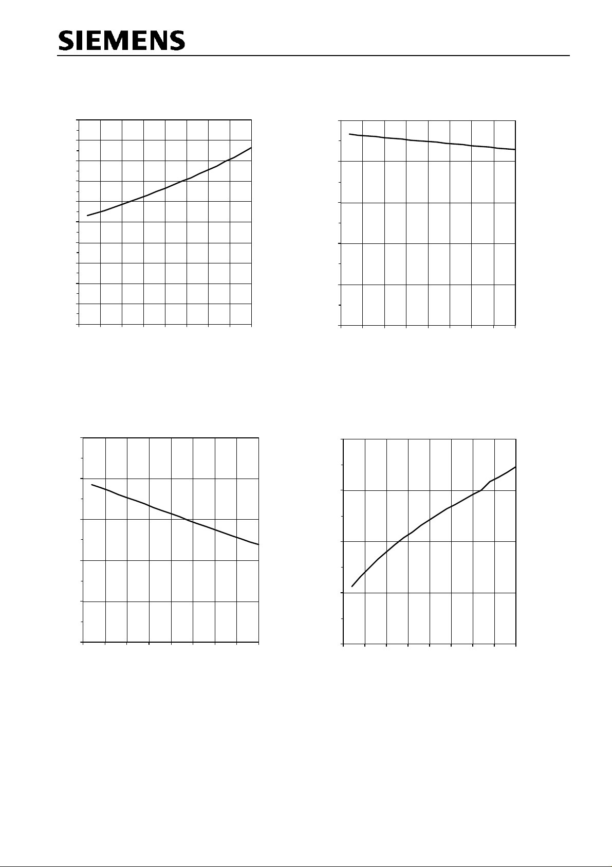
BTS 730
Typ. min. puls duty factor
%
15
14
13
12
11
10
9
8
7
6
5
-50 -25 0 25 50 75 100 125 150
D
im in
= f(
T
)
C
TC °C
Typ. max. puls dut y factor
%
100
99
98
97
96
95
-50 -25 0 25 50 75 100 125 150
D
im ax
= f(
T
)
C
TC °C
Typ. PWM Frequency
Hz
100
90
80
70
60
50
-50 -25 0 25 50 75 100 125 150
f
PWM
= f(
T
)
C
TC °C
Typ. max. output volt age
V
14,0
13,5
13,0
12,5
12,0
V
RMSm ax
-50 -25 0 25 50 75 100 125 150
= f(
T
), Vbb > 12V
C
TC °C
Semiconductor Group 7
 Loading...