

Page 1
AIE Adaptive Image Enhancer Series
Real Time
Video Processor IC
BU1574GUW
●Description
BU1574GUW is AIE : Adaptive Image Enhancer (image processing technology by ROHM’s hardware).
●Features
1) Compatible with image data from QCIF size (176 144) up to WVGA+ size (864 480).
2) Compatible with I/O data formats of ITU-R BT.656-4 or YCbCr with synchronizing signals.
3) Multiple operation modes: Image Enhance, Through and Sleep.
4) Registers can be set up through the 2-wire serial interface (I
5) PWM output for image adjustment LCD backlight control.
6) Built-in edge-enhancement and gamma filters.
●Applications
Car camera, Car display, Car navigation system, Mobile phone, and portable DVD etc.
●Absolute maximum ratings
Parameter Symbol Rating Unit
Power supply voltage 1 VDDIO
Power supply voltage 2 VDD
Input voltage VIN
Storage temperature range Tstg
Power dissipation PD 310*1,570*2 mW
*1 IC only. In the case exceeding 25 °C, 3.1 mW should be reduced per 1 °C.
*2 When mounted on a glass epoxy board of 70 x 70 x 1.6 mm. If exceeding 25 °C, 5.7 mW should be reduced per 1 °C.
* Has not been designed to withstand radiation.
* Operation is not guaranteed.
●Operating conditions
Parameter Symbol Rating Unit
Power supply voltage 1 (IO) VDDIO 2.70~3.60(Typ:3.00) V
Power supply voltage 2 (CORE) VDD 1.40~1.60(Typ:1.50) V
Input voltage range VIN-VDDIO 0~VDDIO V
Operating temperature range Topr -40~+85 ℃
* Supply the power source in order of VDD VDDIO.
2
C).
-0.3~+4.2
-0.3~+2.1
-0.3~VDDIO+0.3
-40~+125 ℃
No.09060EAT04
V
V
V
www.rohm.com
© 2009 ROHM Co., Ltd. All rights reserved.
1/12
2009.06 - Rev.A
Page 2
BU1574GUW
●Electrical characteristics
Parameter Symbol
MIN TYP MAX
Limits
Unit Conditions
Input frequency fIN - - 36.0 MHz CAMCKI (DUTY45%~55%)
Technical Note
Operating current
consumption
Static current consumption IDDst - - 30 uA
IDD1 - 24 - mA At Enhance mode setting (36 MHz).
At Sleep mode setting input terminal= GND
setting
Input "H" current IIH -10 - 10 uA VIH=VDDIO
Input "L" current IIL -10 - 10 uA VIL=GND
Input "H" voltage 1 VIH1
VDDIO
x0.8
-
Input "L" voltage 1 VIL1 -0.3 -
Input "H" voltage 2 VIH2
VDDIO
x0.85
-
Input "L" voltage 2 VIL2 -0.3 -
Hysteresis voltage width Vhys - 0.7 - V
Output "H" voltage VOH
VDDIO
-0.4
- VDDIO V
Output "L" voltage VOL 0.0 - 0.4 V
(Unless otherwise specified; VDD = 1.50 V, VDDIO = 3.00 V, GND = 0.0 V, Ta = 25 ℃, fIN = 36.0 MHz)
VDDIO
+0.3
VDDIO
x0.2
VDDIO
+0.3
VDDIO
x0.15
Normal input
V
(including the input mode of I/O terminal)
Normal input
V
(including the input mode of I/O terminal)
Hysteresis input
V
(RESETB, CAMCKI, SDA, SDC, I2CDEV0)
Hysteresis input
V
(RESETB, CAMCKI, SDA, SDC, I2CDEV0)
Hysteresis input
(RESETB, CAMCKI, SDA, SDC, I2CDEV0)
IOH = -1.0 mA (DC)
(including the output mode of I/O terminal)
IOL = 1.0 mA (DC)
(including the output mode of I/O terminal)
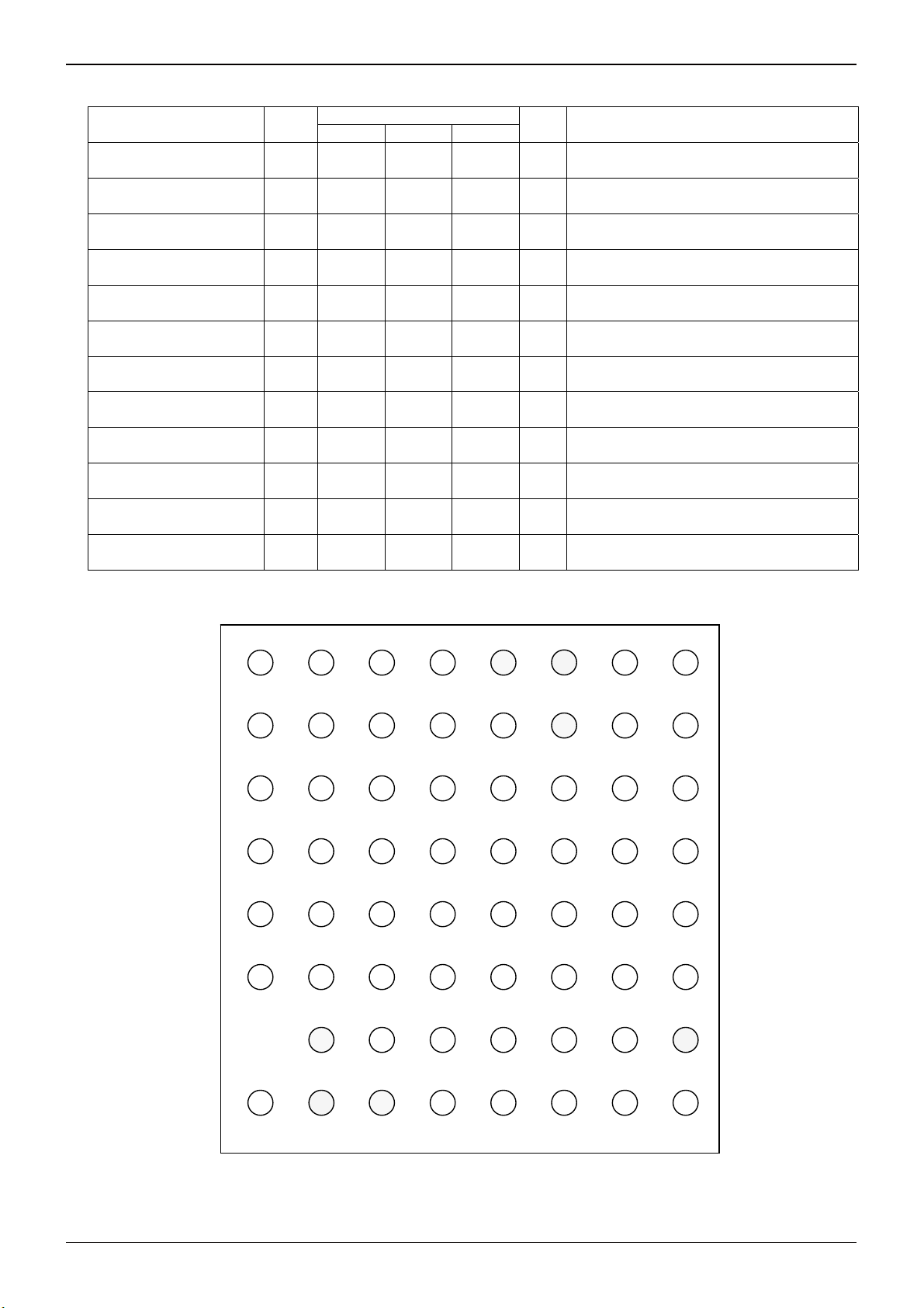
●Terminal Layout
H
17
RESERVEI2
18
RESERVEI3 22RESERVEI724RESERVEI927VDDIO
29
GND
G
15
RESERVEI0
16
RESERVEI1 20RESERVEI521RESERVEI6
25
RESERVEI10
30
VDD
F
13
CAMDI6
14
CAMDI7 19RESERVEI423RESERVEI8
26
RESERVEI1135RESERVEO1136RESERVEO10
E
11
CAMDI49 CAMDI2 10CAMDI312CAMDI528CAMCKI
39
RESERVEO737RESERVEO9
D
8
CAMDI1
5
SDC 7CAMDI060RESETB
44
RESERVEO242RESERVEO441RESERVEO5
C
6
I2CDEV0
4
SDA
3
CAMHSI58CAMHSO55CAMDO051CAMDO4
B
64
VDD 62CAMCKO57RESERVEO1253CAMDO252CAMDO348CAMDO7
A
1
CAMVSI
63
GND
61
VDDIO 59CAMVSO56I2CDEV6B54CAMDO150CAMDO5
1 2 3 4 5 6 7 8
Fig.1 Terminal Layout (Bottom View)
31
MSEL0
32
MSEL1
46
RESERVEO0
33
MSEL2
34
PWMO
38
RESERVEO8
40
RESERVEO6
43
RESERVEO3
45
RESERVEO1
47
GND
49
CAMDO6
www.rohm.com
© 2009 ROHM Co., Ltd. All rights reserved.
2/12
2009.06 - Rev.A
Page 3

BU1574GUW
Technical Note
●Terminal functions
PIN No. Pin Name In/Out Active Level Init Descriptions In/Output type
1 CAMVSI In * - Vertical timing input C*1
2 N.C. *2 - - - - -
3 CAMHSI In * - Horizontal timing input C*1
4 SDA In/Out DATA In In/Output serial data F
5 SDC In CLK - In/Output serial clock D*1
6 I2CDEV0 In * - I2C device address setting D*1
7 CAMDI0 In DATA - Data input: bit 0 G*1
8 CAMDI1 In DATA - Data input: bit 1 G*1
9 CAMDI2 In DATA - Data input: bit 2 G*1
10 CAMDI3 In DATA - Data input: bit 3 G*1
11 CAMDI4 In DATA - Data input: bit 4 G*1
12 CAMDI5 In DATA - Data input: bit 5 G*1
13 CAMDI6 In DATA - Data input: bit 6 G*1
14 CAMDI7 In DATA - Data input: bit 7 G*1
15 RESERVEI0 *3 In * - RESERVE C*1
16 RESERVEI1 *3 In * - RESERVE C*1
17 RESERVEI2 *3 In * - RESERVE C*1
18 RESERVEI3 *3 In * - RESERVE C*1
19 RESERVEI4 *3 In * - RESERVE C*1
20 RESERVEI5 *3 In * - RESERVE C*1
21 RESERVEI6 *3 In * - RESERVE C*1
22 RESERVEI7 *3 In * - RESERVE C*1
23 RESERVEI8 *3 In * - RESERVE C*1
24 RESERVEI9 *3 In * - RESERVE C*1
25 RESERVEI10 *3 In * - RESERVE C*1
26 RESERVEI11 *3 In * - RESERVE C*1
27 VDDIO - PWR - DIGITAL IO power source -
28 CAMCKI In CLK - Clock input D*1
29 GND - GND - Common GROUND -
30 VDD - PWR - CORE power source -
31 MSEL0 *3 In * - Mode select 0 A
32 MSEL1 *3 In * - Mode select 1 A
*Change by setup by the register is possible for the "*" display in the column of an Active level. Moreover, Init is a pin state under reset.
*1 : It suspends during reset (initial state)
*2 : Please connect with GND
*3 : Please connect with GND.
www.rohm.com
© 2009 ROHM Co., Ltd. All rights reserved.
3/12
2009.06 - Rev.A
Page 4

BU1574GUW
Technical Note
PIN No. Pin Name In/Out Active Level Init Descriptions In/Output type
33 MSEL2 *4 In * - Mode select 2 A
34 PWMO Out * Low PWM output for LCD backlight E
35 RESERVEO11 *5 Out * Low RESERVE E
36 RESERVEO10 *5 Out * Low RESERVE E
37 RESERVEO9 *5 Out * Low RESERVE E
38 RESERVEO8 *5 Out * Low RESERVE E
39 RESERVEO7 *5 Out * Low RESERVE E
40 RESERVEO6 *5 Out * Low RESERVE E
41 RESERVEO5 *5 Out * Low RESERVE E
42 RESERVEO4 *5 Out * Low RESERVE E
43 RESERVEO3 *5 Out * Low RESERVE E
44 RESERVEO2 *5 Out * Low RESERVE E
45 RESERVEO1 *5 Out * Low RESERVE E
46 RESERVEO0 *5 Out * Low RESERVE E
47 GND - GND - Common GROUND -
48 CAMDO7 Out DATA Low Data output: bit 7 E
49 CAMDO6 Out DATA Low Data output: bit 6 E
50 CAMDO5 Out DATA Low Data output: bit 5 E
51 CAMDO4 Out DATA Low Data output: bit 4 E
52 CAMDO3 Out DATA Low Data output: bit 3 E
53 CAMDO2 Out DATA Low Data output: bit 2 E
54 CAMDO1 Out DATA Low Data output: bit 1 E
55 CAMDO0 Out DATA Low Data output: bit 0 E
56 I2CDEV6B *3 In * - RESERVE A
57 RESERVEO12 *5 Out * High RESERVE E
58 CAMHSO Out * Low Horizontal timing output signal E
59 CAMVSO Out * Low Vertical timing output signal E
60 RESETB In Low - System reset signal B
61 VDDIO - PWR - DIGITAL IO power source -
62 CAMCKO Out CLK Low Clock output E
63 GND - GND - Common GROUND -
64 VDD - PWR - CORE power source -
*Change by setup by the register is possible for the "*" display in the column of an Active level. Moreover, Init is a pin state under reset.
*3 : Please connect with GND
*4 : Please connect with VDDIO
*5 : Leave OPEN
www.rohm.com
© 2009 ROHM Co., Ltd. All rights reserved.
4/12
2009.06 - Rev.A
Page 5

BU1574GUW
●I/O pins equivalent circuit diagrams
Type Equivalent circuit structure Type Equivalent circuit structure
A
C
E
G
VDDIO
VDDIO
To internal
GND
GND
Input pin
VDDIO
Internal signal
VDDIO
GND
Internal signal
GND
Input pin with the suspend function
VDDIO
VDDIO
Internal signal
GND
GND
Output-pin
VDDIO
Internal signal
VDDIO
GND
To internal
VDDIO
Internal signal
Internal signal
VDDIO
B
GND
Input pin with the hysteresis function
VDDIO
D
GND
Input pin with the hysteresis and suspend functions
VDDIO
To internal
F
GND
In/output pin with the hysteresis function
GND
VDDIO
GND
GND
Internal signal
In/output pin with the suspend function
Fig.2 I/O pins equivalent circuit diagrams
Technical Note
To internal
To internal
Internal signal
Internal signal
Internal signal
Internal signal
www.rohm.com
© 2009 ROHM Co., Ltd. All rights reserved.
5/12
2009.06 - Rev.A
Page 6

BU1574GUW
A
●Block diagram
Technical Note
CAMDI[17:0]
SD
SDC
CAMVSI
CAMHSI
CAMCKI
MSEL0/1/2
RESETB
Color correction
Brightness
distinction
Register
I2C interface
Timing generator
Image enhance
Gamma control
Edge
enhancement
PWM control
generation
CAMDO[17:0]
PWMO
CAMVSO
CAMHSO
CAMCKO
Fig.3 Block diagram
●Functional descriptions
1. Brightness distinction
Luminance of the input image is analyzed, and collection coefficient value is calculated. Calculated collection coefficient
value is kept until the next frame is input, and it is reflected on the image enhancement part and the color collection part
when the next frame is processed.
2. Image enhance
The correction operation is done to the luminance element of the input image based on the correction coefficient value
from the luminance distinction part.
It puts the chroma element from the color correction together, and outputs along output format.
It is possible to change correction strength of the output image.
3. Color correction
The correction operation is done to the chroma element of the input image based on the correction coefficient value from
the luminance distinction part. Color correction strength can be changed.
4. Edge enhancement
The edge emphasis filter is built into. The image is corrected to sharp image quality by emphasizing the outline.
Strength of the edge emphasis filter can be adjusted.
5. Gamma control
Gamma control can be given to the luminance element.
A line form is interpolated with a setup point of the gamma curve between the setup point nine points, and output value is
calculated from that curve.
6. PWM control generation
The PWM signal for the LCD backlight control can be output. There is a setup of a manual by the register in the DUTY
control of the PWM signal, and an auto-setup to be controlled automatically by BU1574GUW. As for the auto-setup,
DUTY is calculated from the luminance information of the input image every frame.
7. Register
The image correction parameter, the image size, and the format are set from the register.
The data of the register can be written by the I
2
C interface, and be read.
www.rohm.com
© 2009 ROHM Co., Ltd. All rights reserved.
6/12
2009.06 - Rev.A
Page 7

BU1574GUW
8. Data input format
8.1 ITU-R BT.656 input format
8.1.1 Horizontal direction synchronization timing
CAMCKI
Technical Note
CAMDI0
-CAMDI7
1st 2nd 3rd 4th Cb0 Y0 Cr0 Y1 Cb359 Y718 Cr359 Y719 1st 2nd 3rd 4th 1st 2nd 3rd 4th
SAV EAV SAV
8.1.2 Vertical direction synchronization timing
Field 1
H bit
V bit
F bit
Field 2
H bit
V bit
F bit
52452512345 19202122
262 263 264 265 266 267 268 282 283 284 285
Fig.5 ITU-R BT.656 input format for NTSC (vertical direction)
Field 1
H bit
622 623 624 625 1 2 3 22 23 24 25
Valid data section
[NTSC] 1716 clocks / [PAL] 1728 clocks
Y: 720
Cb,Cr: 360
1440 clocks
720pixel
data
data
Fig.4 ITU-R BT.656 input format (horizontal direction)
V bit
F bit
Field 2
H bit
V bit
F bit
309 310 311 312 313 314 315 335 336 337 338
Fig.6 ITU-R BT.656 input format for PAL (vertical direction, bottom view)
www.rohm.com
© 2009 ROHM Co., Ltd. All rights reserved.
7/12
2009.06 - Rev.A
Page 8

BU1574GUW
Technical Note
8.2. YCbCr with synchronizing signals 8-bit input format
8.2.1. Horizontal direction synchronization timing
CAMCKI
(*1)
YUV_XST
AIE_XST
×2
XSIZE ×2
AIE_XSIZE ×2
Image area
AIE varid area
CAMDI0
-CAMDI7
(*3)
CAMHSI
Y0 Cb0 Y1 Cr0 Y2 Cb1 Cr1Y3 Cr158 Y318 Y317 Cr158
Y0 Cb0 Y1 Cr0 Y2 Cb1 Cr1Y3 Cr158 Y318 Cb158
(*2)
(*2)
Y318 Cb159 Y319 Cr159Y318
Fig.7 Horizontal direction synchronization timing
(Note)
* YUV_XST, XSIZE x 2, AIE_XST x 2 and AIE_XSIZE×2, which are described in the figures and the notes, are set by the registers.
(*1) By changing the setting of the POL register (INDEX Address: E1h), the polarities of CAMCKI, CAMVSI and CAMHSI can be set independently.
The figure above shows the timing in the case that the data are fetched at the CAMCKI falling edge (CKPOL = 1 setting) and the polarity of
HSYNC is low active (HSPOL = 0 setting).
(*2) Set CAMHSI so as not to become 'L' in other sections than the sync section (CAMHSI = 'L' section in the figure shown above).
(*3) Do not change the frequency of CAMCKI during the operation.
(*4) Take note of the items described above to input each signal.
8.2.2. Vertical direction synchronization timing
YSIZE
AIE_YST line
AIE_YSIZE line
CAMHSI
CAMVSI
CAMDIO
-CAMDI7
Original image
Invalid area
Line.
1
Line.2Line.
3
AIE_YSIZE
-1
AIE_YSIZE
Fig.8 Vertical direction synchronization timing
(Note)
* Y_SIZE, AIE_YST and AIE_YSIZE, which are described in the figures and the notes, are set by the registers.
(*1) The figure above shows the timing in the case that the polarity of VSYNC is low active (VSPOL = 0 setting) and also the polarity of
HSYNC is low active (HSPOL = 0 setting).
(*2) Take note of the items described above to input each signal.
www.rohm.com
© 2009 ROHM Co., Ltd. All rights reserved.
8/12
2009.06 - Rev.A
Page 9
BU1574GUW
2
C Interface format
9. I
Technical Note
The slave address is 42h when I2CDEV0 = 0 and 43h when I2CDEV0 = 1.
When both of the write and read accesses are respectively executed successively 2 times or more, the sub-address is
automatically incremented.
SDA
SDC
START
condition
Write
sequence
Read
sequence
Slave address
S
(42h or 43h)W(0)
Slave address
S
(42h or 43h)
S = START condition A(S) = acknowledge by slave A(S) = not acknowledge by slave
P = STOP condition A(M) = acknowledge by master A(M) = not acknowledge by master
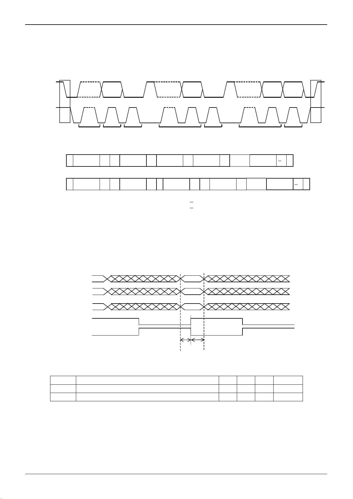
●Timing chart
1. Data input interface timing
CAMVSI
CAMHSI
CAMDI0
-CAMDI7
CAMCKI
(CKPOL-“0”)
CAMCKI
(CKPOL-“1”)
Symbol Descriptions MIN TYP MAX Unit
tDS Setup time to CAMCKI rising / falling edge 8 - - ns
tDH Hold time to CAMCKI rising / falling edge 8 - - ns
Slav e
address
1-7 8S 1-789
R/W
91-789P
Data transfer
A(S) Sub address A(S) Data A(S) Data A(S) Data
W
A(S) Sub address A(S) S
(0)
Fig.9 I
Slave address
(42h or 43h)
2
C Interface format
R
(1)
t
DStDH
Fig.10 Data input interface timing
ACKACK ACKSub address Data
STOP
condition
A(S)/
P
A(S)
A(M)/
A(M) DataA(S) Data
A(M)
P
www.rohm.com
© 2009 ROHM Co., Ltd. All rights reserved.
9/12
2009.06 - Rev.A
Page 10

BU1574GUW
I
C
2. Data output interface timing
CAMCKO
t
PCLK
Technical Note
CAMVSO
t
OCD
t
OCD
CAMHSO
t
ODD
CAMDO[7:0]
Fig.11 Data output interface timing
Symbol Descriptions MIN TYP MAX Unit
tPCLK Clock cycle 27.7 - - ns
dPCLK Clock duty 40 50 60 %
tODD CAMDO is defined from CAMCKO - - 5 ns
tOCD CAMVSO and CAMHSO are defined from CAMCKO - - 5 ns
2
C interface timing
3. I
SDA
t
SU;D AT
t
HD;DATtHIGH
Fig.12 I
t
SU;S TA
2
C interface timing
t
HD;ST
t
SU;S TO
t
BUF
SDC
t
HD;STA
t
LOW
Symbol Descriptions MIN TYP MAX Unit
fSCL SDC clock frequency 0 - 400 kHz
tHD;STA
Hold time (repeat) "START" condition
The first clock pulse is generated after this period
0.6 - - µs
fLOW SDC clock "L" period 1.3 - - µs
tHIGH SDC clock "H" period 0.6 - - µs
tSU;STA Repeat "START" condition setup time 0.6 - - µs
tHD;DAT Data hold time 0 µs
tSU;DAT Data setup time 100 - - ns
tSU;STO "STOP" condition setup time 0.6 - - µs
tBUF Bus free period between the "STOP" condition and "START" condition 1.3 - - µs
●Application example
CAMDO[7:0]
AMHSO
CAMVSO
CAMCKO
Image
pro cess ing
C
Camera
module
CAMDI[7:0]
CAMHSI
CAMVSI
CAMCKI
SDA
SDC
CAMDOI[7:0]
CAMHSI
BU15 74GUW
CAMVSI
CAMCKI
CAMDO[7:0]
CA MHS O
CA MVS O
CA MCK O
Fig.13 Application example
www.rohm.com
© 2009 ROHM Co., Ltd. All rights reserved.
10/12
2009.06 - Rev.A
Page 11

BU1574GUW
Technical Note
●Notes for use
(1) Absolute Maximum Ratings
An excess in the absolute maximum ratings, such as supply voltage, temperature range of operating conditions, etc., can break
down devices, thus making impossible to identify breaking mode such as a short circuit or an open circuit. If any special mode
exceeding the absolute maximum ratings is assumed, consideration should be given to take physical safety measures including
the use of fuses, etc.
(2) Operating conditions
These conditions represent a range within which characteristics can be provided approximately as expected. The electrical
characteristics are guaranteed under the conditions of each parameter.
(3) Reverse connection of power supply connector
The reverse connection of power supply connector can break down ICs. Take protective measures against the breakdown due
to the reverse connection, such as mounting an external diode between the power supply and the IC’s power supply terminal.
(4) Power supply line
Design PCB pattern to provide low impedance for the wiring between the power supply and the GND lines.
In this regard, for the digital block power supply and the analog block power supply, even though these power supplies has the
same level of potential, separate the power supply pattern for the digital block from that for the analog block, thus suppressing
the diffraction of digital noises to the analog block power supply resulting from impedance common to the wiring patterns. For
the GND line, give consideration to design the patterns in a similar manner.
Furthermore, for all power supply terminals to ICs, mount a capacitor between the power supply and the GND terminal. At the
same time, in order to use an electrolytic capacitor, thoroughly check to be sure the characteristics of the capacitor to be used
present no problem including the occurrence of capacity dropout at a low temperature, thus determining the constant.
(5) GND voltage
Make setting of the potential of the GND terminal so that it will be maintained at the minimum in any operating state.
Furthermore, check to be sure no terminals are at a potential lower than the GND voltage including an actual electric transient.
(6) Short circuit between terminals and erroneous mounting
In order to mount ICs on a set PCB, pay thorough attention to the direction and offset of the ICs. Erroneous mounting can break
down the ICs. Furthermore, if a short circuit occurs due to foreign matters entering between terminals or between the terminal
and the power supply or the GND terminal, the ICs can break down.
(7) Operation in strong electromagnetic field
Be noted that using ICs in the strong electromagnetic field can malfunction them.
(8) Inspection with set PCB
On the inspection with the set PCB, if a capacitor is connected to a low-impedance IC terminal, the IC can suffer stress.
Therefore, be sure to discharge from the set PCB by each process. Furthermore, in order to mount or dismount the set PCB
to/from the jig for the inspection process, be sure to turn OFF the power supply and then mount the set PCB to the jig. After the
completion of the inspection, be sure to turn OFF the power supply and then dismount it from the jig. In addition, for protection
against static electricity, establish a ground for the assembly process and pay thorough attention to the transportation and the
storage of the set PCB.
(9) Input terminals
In terms of the construction of IC, parasitic elements are inevitably formed in relation to potential. The operation of the parasitic
element can cause interference with circuit operation, thus resulting in a malfunction and then breakdown of the input terminal.
Therefore, pay thorough attention not to handle the input terminals, such as to apply to the input terminals a voltage lower than
the GND respectively, so that any parasitic element will operate. Furthermore, do not apply a voltage to the input terminals when
no power supply voltage is applied to the IC. In addition, even if the power supply voltage is applied, apply to the input terminals
a voltage lower than the power supply voltage or within the guaranteed value of electrical characteristics.
(10) Ground wiring pattern
If small-signal GND and large-current GND are provided, It will be recommended to separate the large-current GND pattern
from the small-signal GND pattern and establish a single ground at the reference point of the set PCB so that resistance to the
wiring pattern and voltage fluctuations due to a large current will cause no fluctuations in voltages of the small-signal GND. Pay
attention not to cause fluctuations in the GND wiring pattern of external parts as well.
(11) External capacitor
In order to use a ceramic capacitor as the external capacitor, determine the constant with consideration given to a degradation
in the nominal capacitance due to DC bias and changes in the capacitance due to temperature, etc.
www.rohm.com
© 2009 ROHM Co., Ltd. All rights reserved.
11/12
2009.06 - Rev.A
Page 12

BU1574GUW
●Ordering part number
B U 1 5 7 4 G U W - E 2
ROHM model
name
●Package specification
VBGA063W050
1PIN MARK
0.08 S
63-φ0.295±0.05
M
φ
0.05
Product number Package type
5.0±0.1
5.0± 0.1
0.10
S
0.9MAX
0.75±0.1
P=0.5×7
0.5
ABS
A
H
G
F
E
D
C
B
A
B
0.5
51
3
762
4
P=0.5×7
8
0.75±0.1
(Unit : mm)
<Tape and Reel information>
Quantity
Direction
of feed
Taping model name
GUW: VBGA063W050
Embossed carrier tape (with dry pack)Tape
2500pcs
E2
The direction is the 1pin of product is at the upper left when you hold
()
reel on the left hand and you pull out the tape on the right hand
Reel
1pin
Order quantity needs to be multiple of the minimum quantity.
∗
E2: Embossed reel tape
Technical Note
Direction of feed
www.rohm.com
© 2009 ROHM Co., Ltd. All rights reserved.
12/12
2009.06 - Rev.A
Page 13

Notes
No copying or reproduction of this document, in part or in whole, is permitted without the
consent of ROHM Co.,Ltd.
The content specied herein is subject to change for improvement without notice.
The content specied herein is for the purpose of introducing ROHM's products (hereinafter
"Products"). If you wish to use any such Product, please be sure to refer to the specications,
which can be obtained from ROHM upon request.
Examples of application circuits, circuit constants and any other information contained herein
illustrate the standard usage and operations of the Products. The peripheral conditions must
be taken into account when designing circuits for mass production.
Great care was taken in ensuring the accuracy of the information specied in this document.
However, should you incur any damage arising from any inaccuracy or misprint of such
information, ROHM shall bear no responsibility for such damage.
The technical information specied herein is intended only to show the typical functions of and
examples of application circuits for the Products. ROHM does not grant you, explicitly or
implicitly, any license to use or exercise intellectual property or other rights held by ROHM and
other par ties. ROHM shall bear no responsibility whatsoever for any dispute arising from the
use of such technical information.
Notice
The Products specied in this document are intended to be used with general-use electronic
equipment or devices (such as audio visual equipment, ofce-automation equipment, communication devices, electronic appliances and amusement devices).
The Products specied in this document are not designed to be radiation tolerant.
While ROHM always makes efforts to enhance the quality and reliability of its Products, a
Product may fail or malfunction for a variety of reasons.
Please be sure to implement in your equipment using the Products safety measures to guard
against the possibility of physical injury, re or any other damage caused in the event of the
failure of any Product, such as derating, redundancy, re control and fail-safe designs. ROHM
shall bear no responsibility whatsoever for your use of any Product outside of the prescribed
scope or not in accordance with the instruction manual.
The Products are not designed or manufactured to be used with any equipment, device or
system which requires an extremely high level of reliability the failure or malfunction of which
may result in a direct threat to human life or create a risk of human injury (such as a medical
instrument, transpor tation equipment, aerospace machinery, nuclear-reactor controller,
fuel-controller or other safety device). ROHM shall bear no responsibility in any way for use of
any of the Products for the above special purposes. If a Product is intended to be used for any
such special purpose, please contact a ROHM sales representative before purchasing.
If you intend to export or ship overseas any Product or technology specied herein that may
be controlled under the Foreign Exchange and the Foreign Trade Law, you will be required to
obtain a license or permit under the Law.
Thank you for your accessing to ROHM product informations.
More detail product informations and catalogs are available, please contact us.
ROHM Customer Support System
www.rohm.com
© 2009 ROHM Co., Ltd. All rights reserved.
http://www.rohm.com/contact/
R0039
A
 Loading...