


1
Multimedia ICs
NTSC / PAL digital RGB encoder
BU1425AK / BU1425AKV
The BU1425AK / BU1425AKV are ICs which convert digital RGB / YUV input to composite (NTSC / PAL / PAL60),
luminance (Y), and chrominance (C) signals, and outputs the results.
•
Applications
Video interfaces for VIDEO-CDs and CD-G decoders
•
Features
1) Input clocks supported
27.0 / 13.5MHz
28.636 / 14.318MHz
28.375 / 14.1875MHz
35.4695 / 17.73475MHz
2) 24-bit RGB and 16-bit YUV input signals are supported.
3) Both master and slave systems are supported.
4) 9-bit high-speed DAC is used for DAC output of
composite VIDEO, Y, and C signals.
5) Internal 8-color OSD output function is provided.
6) FSC-TRAP on the Y channel can be turned on and
off.
7) C channel is equipped with an internal chrominance band-pass filter in addition to the U.V. lowpass filter.
8) 5V single power supply, low power consumption
(0.4W typ.)
9) Y and C output can be turned off (the power consumption with Y and C off is 0.25W typ.).
10) In the Master mode, applying 3.3V to the I / O V
DD
and 5.0V to other VDDs produces HSY and VSY
output with an amplitude of 3.3V. This enables
direct connection to LSIs that use a power supply
voltage of 3.3V. (The clock output for the OSD has
a fixed amplitude of 5.0V.)
11) In the Slave mode, applying voltage to the I / O V
DD
only, and applying 0V to other VDDs, enables a current consumption of 0 even when RGB DATA,
HSY, VSY, and OSD DATA are in the active state.

2
Multimedia ICs BU1425AK / BU1425AKV
•
Block diagram
BOSD
GOSD
ROSD
OSDSW
OSD PALETTE
RGB 24BITS
Y-FILTER MIX SIG
and
sync
burst
DAC
V
Y
C
C-FILTER
Y-LEVEL ADJ
CHROMA GEN
UV
FILTER
LATCH
RD
GD / Y
BD / UV
VCLK
RSTB
VIDEO TIMING CONTROL
SYNC BLANK
BURST
SUB CARRIER BURST GENERATOR
MODE CONTROL FIELD / FLAME CONTROL
VOUT
YOUT
COUT
PIXCLK
HSY
VSY
RGB
to
YUV
TEST12
ADDH
INT
IM [0.1]
YFILONB [1.0]
CDGSWB
PAL60B
NTB
CLKSW

3
Multimedia ICs BU1425AK / BU1425AKV
•
Pin descriptions
Pin No.
Pin name
Function
1
2
3
4
5
6
7
8
9
10
11
12
13
14
15
16
17
18
19
20
21
22
23
24
25
26
27
28
29
30
31
32
∗
With pull-down resistor (approx. 30kΩ )
∗
BOSD
GD0 / Y0
GD1 / Y1
GD2 / Y2
GD3 / Y3
GD4 / Y4
GD5 / Y5
GD6 / Y6
GND
GD7 / Y7
BD0 / UV0
BD1 / UV1
BD2 / UV2
BD3 / UV3
OSDSW
CDGSWB
BD4 / UV4
BD5 / UV5
BD6 / UV6
BD7 / UV7
GND
NTB
IM0
IM1
TEST1
TEST2
VSY
HSY
PIXCLK
VDD
IOVDD
INT
33
34
35
36
37
38
39
40
41
42
43
44
45
46
47
48
49
50
51
52
53
54
55
56
57
58
59
60
61
62
63
64
SLABEB
ADDH
VREF-C
CGND
COUT
VGND
VOUT
AV
SS
P-VDD
IR
AV
DD
YGND
YOUT
V
DD
YFILON2B
YCOFF
YFILON1B
PAL60B
VCLK
RSTB
CLKSW
RD0
RD1
RD2
ROSD
RD3
RD4
RD5
IOV
DD
RD6
RD7
GOSD
OSD BLUE DATA INPUT
GREEN DATA Bit0 (LSB)
GREEN DATA Bit1
GREEN DATA Bit2
GREEN DATA Bit3
GREEN DATA Bit4
GREEN DATA Bit5
GREEN DATA Bit6
DIGITAL GROUND
GREEN DATA Bit7 (MSB)
BLUE DATA Bit0 (LSB)
BLUE DATA Bit1
BLUE DATA Bit2
BLUE DATA Bit3
OSD ENABLE / DISABLE
SELECT Video-CD / CD-G
BLUE DATA Bit4
BLUE DATA Bit5
BLUE DATA Bit6
BLUE DATA Bit7 (MSB)
DIGITAL GROUND
SELECT NTSC / PAL MODE
SELECT YUV / RGB
SELECT DAC / NORMAL
Normally pull down to GND
SELECT U / V TIMING
V-SYNC INPUT or OUTPUT
H-SYNC INPUT or OUTPUT
1 / 2freq. of BCLK
DIGITAL V
DD
VDD for I / O
Interlace / Non-Interlace
Pin No.
Pin name
SELECT MASTER / SLAVE
+ 0.5 / – 0.5LINE at NON-INTER
DAC BIAS
CHROMA OUTPUT GROUND
CHROMA OUTPUT
Composite Output Ground
COMPOSITE OUTPUT
Analog Ground (DAC VREF)
POWER (DAC) V
DD
REFERENCE RESISTOR
ANALOG (VREF) V
DD
Luminance Output Ground
Luminance Output
DIGITAL V
DD
Y-FILSEL THROU / FILON2
DAC (YOUTCOUT) OFF
Y-FILSEL THROU / FILON1
NORMAL / PAL60 at PALMODE
Video Clock Input
NORMAL / RESET
SEL ×1CLK / ×2CLK
RED DATA Bit0 (LSB)
RED DATA Bit1
RED DATA Bit2
OSD RED DATA INPUT
RED DATA Bit3
RED DATA Bit4
RED DATA Bit5
V
DD for I / O
RED DATA Bit6
RED DATA Bit7
OSDGREEN DATA INPUT
Function
4
Multimedia ICs BU1425AK / BU1425AKV
•
Absolute maximum ratings (Ta = 25°C)
Parameter Symbol Limits Unit
Applied voltage
Input voltage
Storage temperature
Power dissipation
V
DD
, AV
DD
V
IN
Tstg
Pd
– 0.5 ~ + 7.0
– 0.3 ~ IOV
DD
+ 0.3
– 55 ~ + 150
1350
∗
1
V
V
°C
mW
∗
1 Reduced by 11mW for each increase in Ta of 1°C over 25°C.
∗
1 When mounted on 120mm × 140mm × 1.0mm glass epoxy board.
∗
Operation is not guaranteed at this value.
䊊
Not designed for radiation resistance.
•
Recommended operating conditions
Parameter Symbol Limits Unit
Power supply voltage
Power supply voltage
Input high level voltage
Input low level voltage
Analog input voltage
Operating temperature
V
DD
= AV
DD
∗
IOV
DD
V
IH
V
IL
V
AIN
Topr
0 ~ + 0.8
0 ~ AV
DD
– 25 ~ + 60
4.50 ~
3.30 ~
2.1 ~
5.50
5.50
V
DD
V
V
V
V
V
°C
∗
Should be used at VDD = AVDD.
•
Electrical characteristics (unless otherwise noted, Ta = 25°C, VDD = AVDD = 5.0V, GND = AVSS = VGND = CGND = YGND)
Parameter
Symbol Min. Typ. Max. Unit Conditions
〈Digital block〉
Burst frequency 1
Burst frequency 2
Burst cycle
Operating circuit current 1
Operating circuit current 2
Output high level voltage
Output low level voltage
Input high level voltage
Input low level voltage
Input high level current
Input low level current
fBST1
fBST2
CBST
Idd1
Idd2
V
OH
V
OL
V
IH
V
IL
I
IH
I
IL
—
—
—
—
—
4.0
—
2.1
—
3.57954
4.43361
9
80
40
4.5
0.5
—
—
0.0
0.0
—
—
—
—
—
—
1.0
—
0.8
10.0
10.0
MHz
MHz
CYC
mA
mA
V
V
V
V
µA
µA
27MHz color bar
27MHz color bar PD mode
I
OH
= – 2.0mA
I
OH
= 2.0mA
– 10
– 10
〈DAC block〉
DAC resolution
Linearity error
Y white level current
Y black level current
Y zero level current
V white level current
V black level current
V zero level current
RES
EL
IYW
IYB
IYZ
IYW
IYB
IYZ
—
—
—
—
—
—
9
25.14
7.24
0.0
25.14
7.24
0.0
—
—
—
10.0
—
—
10.0
BITS
LSB
mA
mA
µA
mA
mA
µA
IR = 1.2kΩ
Sleep mode current Iddpd — — 1.0 µA
V
IN
Max. = IOVDD + 0.3V
V
IN
Min. = – 0.3V
– 10
– 10
± 0.5 ± 3.0
5
Multimedia ICs BU1425AK / BU1425AKV
•
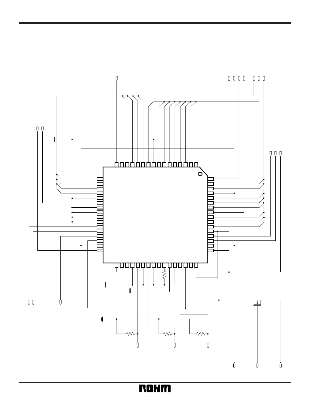
Application example
(1) Example in Master mode: Doubled clock is input and 24-bit RGB input is used
1234567
8
9
10
11
12
13
14
15
16
48
47
46
45
44
43
42
41
40
39
38
37
36
35
34
33
17
18
19
20
21
22
23
24
25
26
27
28
29
30
31
32
7
6543210
3
7
6
5
4
6
7
4
3
5
1
0
2
210
B Data 0...7
G Data 0...7
R Data 0...7
[Blue]
[Green]
[Red]
OSD in
Vsync out
Hsync out
OSD CLOCK
75
75
75
OSD in
OSD in
Video-CD / CD-G
64
63
62
61
60
59
58
57
56
55
54
53
52
51
50
49
Reset [Low active] in
Pixel Clock in
Y-filter select
INTERLACE / NON-INTER
PAL / NTSC
DIGITAL GND
Chrominance
Composite
Luminance
MAIN V
DD
5.0 V
SLEEP MODE CTL
L: SLEEP
H: NORMAL
I / O V
DD
5.0V or 3.3V
BU1425AK / AKV
ANALOG VDD
1.2k
0.01µF
ANALOG GND
POWER GND
POWER VDD
DIGITAL VDD
CDGSWB
OSDSW
BD3
BD2
BD1
BD0
GD7
GND
GD6
GD5
GD4
GD3
GD2
GD1
GD0
BOSD
SLABEB
ADDH
VREF
CGND
COUT
VGND
V
OUT
AVSSAVDDIR
AVDDYGND
YOUT
VDDYFILON2B
YCOFF
BD4
BD5
BD6
BD7
GND
NTB
IM0
IM1
TEST1
TEST2
VSY
HSY
PIXCLK
V
DD
I / O VDD
INT
GOSD
RD7
RD6
I / O V
DD
RD5
RD4
RD3
ROSD
RD2
RD1
RD0
CLKSW
RSTB
VCLK
PAL GOB
YFILON1B
OSD enable
Fig.1
6
Multimedia ICs BU1425AK / BU1425AKV
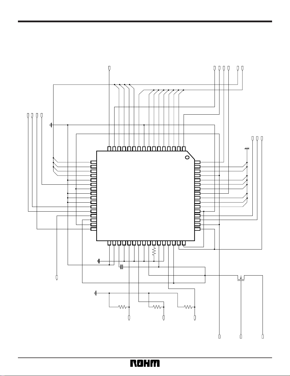
(2) Example in Slave mode: Doubled clock is input and 16-bit YUV input is used
1234567
8
9
10
11
12
13
14
15
16
48
47
46
45
44
43
42
41
40
39
38
37
36
35
34
33
17
18
19
20
21
22
23
24
25
26
27
28
29
30
31
32
7
6543210
3
7
6
5
4
6
7
4
3
5
1
0
2
210
U.V Data 0...7
Y Data 0...7
[Blue]
[Green]
[Red]
OSD in
OSD CLOCK
75
75
75
OSD in
OSD in
Video-CD / CD-G
64
63
62
61
60
59
58
57
56
55
54
53
52
51
50
49
Reset [Low active] in
Pixel Clock in
Y-filter select
INTERLACE / NON-INTER
PAL / NTSC
DIGITAL GND
Hsync in
Vsync in
Chrominance
Composite
Luminance
MAIN V
DD
5.0V
SLEEP MODE CTL
L: SLEEP
H: NORMAL
I / 0 V
DD
5.0V or 3.3V
BU1425AK / AKV
ANALOG VDD
0.01µF
ANALOG GND
POWER GND
POWER VDD
DIGITAL VDD
CDGSWB
OSDSW
BD3
BD2
BD1
BD0
GD7
GND
GD6
GD5
GD4
GD3
GD2
GD1
GD0
BOSD
SLABEB
ADDH
VREF
CGND
COUT
VGND
V
OUT
AVSSAVDDIR
AVDDYGND
YOUT
VDDYFILON2B
YCOFF
BD4
BD5
BD6
BD7
GND
NTB
IM0
IM1
TEST1
TEST2
VSY
HSY
PIXCLK
V
DD
I / O VDD
INT
GOSD
RD7
RD6
I / O V
DD
RD5
RD4
RD3
ROSD
RD2
RD1
RD0
CLKSW
RSTB
YCLK
PAL GOB
YFILON1B
1.2k
Fig.2
OSD enable

7
Multimedia ICs BU1425AK / BU1425AKV
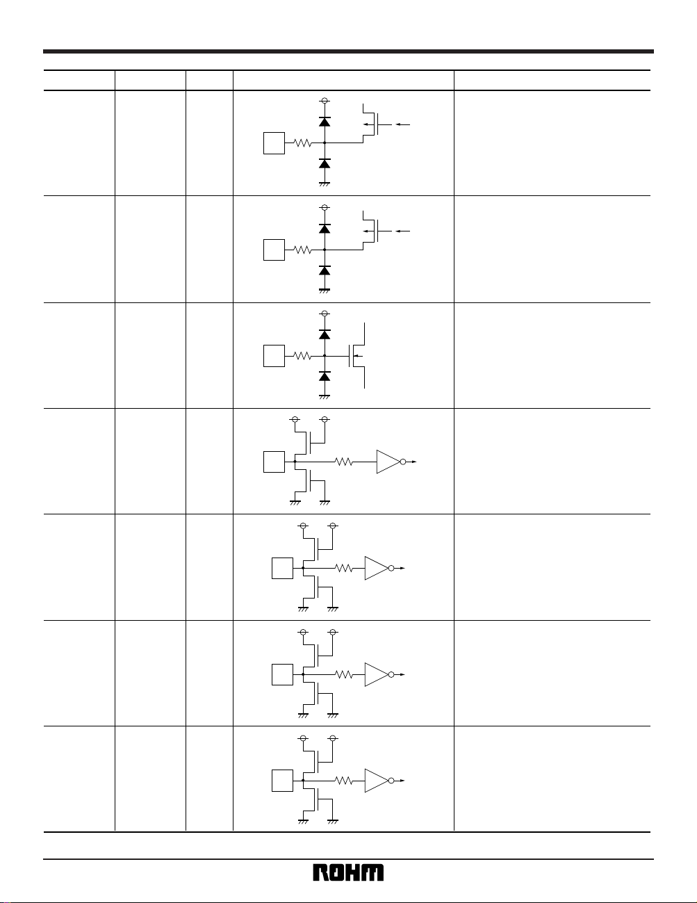
•
Equivalent circuits
Pin No. Pin name Equivalent circuitI / O Function
2 ~ 8
10
GD (7: 0)
G data input pin for 24-bit RGB input
Y data input pin for 16-bit YUV input
11 ~ 14
17 ~ 20
BD (0: 7)
B data input pin for 24-bit RGB input
U, V data input pins for 16-bit YUV
input
Control pins used to select RGB (24bit), YUV (16-bit) or DAC Through as
the input mode.
16 CDGSWB
Switches the mode between VideoCD (HIGH) and CD-G (LOW).
54 ~ 56
58 ~ 60
62.63
RD (0: 7)
R data input pin for 24-bit RGB input
1
57
64
15
ROSD
GOSD
BOSD
OSDSW
OSD data input pin when using the
OSD function.
When the OSDSW pin is HIGH, input
to the ROSD, GOSD, and BOSD pins
takes precedence over RGB, and the
data is converted.
23
24
IM0
IM1
22 NTB
Switches the mode between NTSC
(LOW) and PAL (HIGH).
I
I
I
I
I
I
I
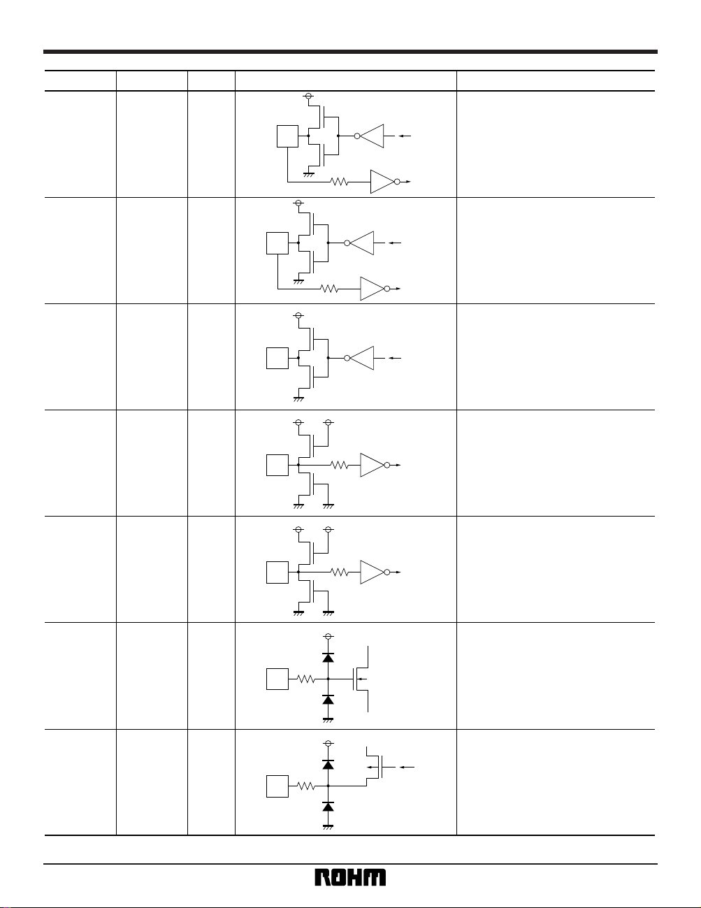
8
Multimedia ICs BU1425AK / BU1425AKV
Pin No. Pin name Equivalent circuitI / O Function
27 VSY I / O
Vertical synchronization signals (Vsync)
are input (when SLABEB = LOW) or
output (when SLABEB = HIGH) here.
35 VREF-C I
This is the reference voltage generator
circuit monitoring pin which determines the output amplitude (output current for 1 LSB) of the DAC. A 0.01µF
capacitor should be attached between
this and pin 43 (AV
DD).
29 PIXCLK O
The internal processing clock is divided in half and output. Data is read at
the point at which the edge of this
clock changes. This can also be used
as the clock for the OSD IC.
32 INT I
This pin switches between interlace
(when HIGH) and non-interlace (when
LOW) modes. This pin is effective in
both the VIDEO-CD and CD-G
modes.
33
34
SLABEB
ADDH
I
I
This pin switches between the Master
(when HIGH) and Slave (when LOW)
modes. It is effective in the noninterlace mode, and it switches between – 0.5 lines (when LOW) and + 0.5
lines (when HIGH) for the number of
lines in an interlace field.
28 HSY I / O
This is the horizontal synchronization
signal pin. Negative polarity Hsync
signals are input (when SLABEB =
LOW) or output (when SLABEB =
HIGH) here. This is also used as the
synchronization signal for fixing the
PIXCLK output phase.
37 COUT O
This is the chrominance output pin for
the S pin.
9
Multimedia ICs BU1425AK / BU1425AKV
Pin No. Pin name Equivalent circuitI / O Function
39 VOUT O
Composite output pin
45 YOUT O
Luminance output pin for the S pin
42 IR I
The output amplitude (output current
for 1 LSB) of the DAC is specified
using an external resistor, and this pin
controls the value of the current flowing per bit.
48 YCOFF I
When there is HIGH input at the signal
input pin which switches to and from
the low power consumption mode, this
turns off the output from the YOUT
and COUT pins.
51
49
VCLK
Input pin for the reference clock in the
Video-CD mode
52 RSTB
Reset input pin which initializes the
system. The system is reset when
this goes LOW.
YFILON1B
YFILON2B
Selects the F characteristic of the
Y-FILTER.
I
I
I

10
Multimedia ICs BU1425AK / BU1425AKV
Pin No. Pin name Equivalent circuitI / O Function
53 CLKSW I
50 PAL60B
Switches between the PAL and PAL60
modes. This is effective only when
the NTB pin is HIGH. (PAL mode
only)
This switches between dividing the
VCLK input in half and using it as an
internal clock (when LOW), and using
it as an internal clock without dividing
it in half (when HIGH).
25
26
TEST1
TEST2
I
Normally, this is connected to the
GND pin. However, when 16-bit YUV
input is used, the TEST2 pin can be
used as the U and V timing control
pins.
I
31
46
61
41
43
AV
DD
IOVDD
Power supply pin for the digital, the
analog, and I / O blocks
9
21
36
38
40
44
GND
CGND
VGND
AV
SS
YGND
Grounding pin for the digital and
analog blocks
30 VDD
Digital VDD. Equipped with pull-down
resistor.
 Loading...