


R&S®RTO-K91, R&S®RTO6-K91,
R&S®RTP-K91
DDR3 Compliance Test
User Manual
(;ÜåÕ2)
1178877102
Version 07

This document describes the following DDR3 Compliance Test Procedures:
●
R&S®RTO-K91 (1337.8891.02)
●
R&S®RTO6-K91 (1801.6993.02)
●
R&S®RTP-K91 (1337.8840.02)
© 2021 Rohde & Schwarz GmbH & Co. KG
Mühldorfstr. 15, 81671 München, Germany
Phone: +49 89 41 29 - 0
Email: info@rohde-schwarz.com
Internet: www.rohde-schwarz.com
Subject to change – data without tolerance limits is not binding.
R&S® is a registered trademark of Rohde & Schwarz GmbH & Co. KG.
Trade names are trademarks of the owners.
1178.8771.02 | Version 07 | R&S®RTO-K91, R&S®RTO6-K91, R&S®RTP-K91
Throughout this manual, products from Rohde & Schwarz are indicated without the ® symbol , e.g. R&S®ScopeSuite is indicated as
R&S ScopeSuite.

R&S®RTO-K91, R&S®RTO6-K91, R&S®RTP-K91
Contents
1 R&S ScopeSuite Overview....................................................................7
2 Preparing the Measurements................................................................9
2.1 Test Equipment..............................................................................................................9
2.1.1 Soldering Guide for Modular Probes...............................................................................9
2.2 Installing Software and License.................................................................................. 9
2.3 Setting Up the Network...............................................................................................10
2.4 Starting the R&S ScopeSuite..................................................................................... 11
2.5 Connecting the R&S RTO/RTO6/RTP........................................................................ 11
2.6 Report Configuration.................................................................................................. 13
3 Performing Tests..................................................................................14
Contents
3.1 Starting a Test Session...............................................................................................14
3.2 Configuring the Test................................................................................................... 15
3.2.1 General Test Settings....................................................................................................16
3.2.2 Test Configuration for DDR3......................................................................................... 18
3.3 Initiating the Test.........................................................................................................21
3.4 Getting Test Results....................................................................................................22
3.5 Starting DDR3 Tests....................................................................................................23
4 Timing Tests......................................................................................... 24
4.1 Clock Timing................................................................................................................24
4.1.1 Test Equipment............................................................................................................. 24
4.1.2 Performing the Tests..................................................................................................... 24
4.1.3 Test Setup..................................................................................................................... 25
4.1.4 Measurements.............................................................................................................. 25
4.2 Data Timing..................................................................................................................27
4.2.1 Test Equipment............................................................................................................. 27
4.2.2 Performing the Tests..................................................................................................... 27
4.2.3 Test Setup..................................................................................................................... 28
4.2.4 Measurements.............................................................................................................. 29
4.3 Strobe Timing.............................................................................................................. 30
4.3.1 Test Equipment............................................................................................................. 30
3User Manual 1178.8771.02 ─ 07

R&S®RTO-K91, R&S®RTO6-K91, R&S®RTP-K91
4.3.2 Performing the Tests..................................................................................................... 30
4.3.3 Test Setup..................................................................................................................... 31
4.3.4 Measurements.............................................................................................................. 32
4.4 Command Timing........................................................................................................34
4.4.1 Test Equipment............................................................................................................. 34
4.4.2 Performing the Tests..................................................................................................... 34
4.4.3 Test Setup..................................................................................................................... 35
4.4.4 Measurements.............................................................................................................. 36
4.5 Address Timing........................................................................................................... 37
4.5.1 Test Equipment............................................................................................................. 37
4.5.2 Performing the Tests..................................................................................................... 37
4.5.3 Measurements.............................................................................................................. 38
4.6 Chip Select Timing......................................................................................................39
Contents
4.6.1 Test Equipment............................................................................................................. 39
4.6.2 Performing the Tests..................................................................................................... 39
4.6.3 Test Setup..................................................................................................................... 40
4.6.4 Measurements.............................................................................................................. 40
4.7 Clock Enable Timing...................................................................................................41
4.7.1 Test Equipment............................................................................................................. 41
4.7.2 Performing the Tests..................................................................................................... 41
4.7.3 Test Setup..................................................................................................................... 42
4.7.4 Measurements.............................................................................................................. 42
5 Electrical Tests..................................................................................... 44
5.1 Single-Ended Signals................................................................................................. 44
5.1.1 Input Slew Rate for ADD and CMD...............................................................................44
5.1.2 Input Slew Rate for DQ and DM....................................................................................46
5.1.3 AC & DC Input Levels for ADD and CMD..................................................................... 48
5.1.4 AC Input Levels for CK and DQS..................................................................................50
5.1.5 Output Slew Rate for DQ.............................................................................................. 52
5.1.6 AC & DC Output Levels for DQ.....................................................................................53
5.1.7 AC Overshoot & Undershoot for ADD and CMD...........................................................55
5.1.8 AC Overshoot & Undershoot for CK, DQ, DQS, and DM..............................................57
5.2 Differential Signals......................................................................................................59
4User Manual 1178.8771.02 ─ 07

R&S®RTO-K91, R&S®RTO6-K91, R&S®RTP-K91
5.2.1 AC Input Levels for CK and DQS..................................................................................59
5.2.2 AC Differential Cross Point Voltage for CK................................................................... 61
5.2.3 Differential Output Slew Rate for DQS..........................................................................63
5.2.4 Differential AC Output Levels for DQS..........................................................................65
6 Debug Tests..........................................................................................68
6.1 Trigger Write Cycle......................................................................................................68
6.1.1 Test Equipment............................................................................................................. 68
6.1.2 Performing the Tests..................................................................................................... 68
6.1.3 Test Setup..................................................................................................................... 69
6.1.4 Measurements.............................................................................................................. 69
6.2 Trigger Read Cycle......................................................................................................69
6.2.1 Test Equipment............................................................................................................. 69
Contents
6.2.2 Performing the Tests..................................................................................................... 69
6.2.3 Test Setup..................................................................................................................... 70
6.2.4 Measurements.............................................................................................................. 70
5User Manual 1178.8771.02 ─ 07

R&S®RTO-K91, R&S®RTO6-K91, R&S®RTP-K91
Contents
6User Manual 1178.8771.02 ─ 07

R&S®RTO-K91, R&S®RTO6-K91, R&S®RTP-K91
1 R&S ScopeSuite Overview
The R&S ScopeSuite software is used with R&S RTO/RTO6/RTP oscilloscopes. It can
be installed on a test computer or directly on the oscilloscope. For system requirements, refer to the Release Notes.
R&S ScopeSuite Overview
The R&S ScopeSuite main panel has several areas:
●
"Settings": connection settings to oscilloscope and other instruments also default
report settings
●
"Compliance Tests": selection of the compliance test
●
"Demo": accesses demo test cases that can be used for trying out the software
without having a connection to an oscilloscope
●
"Help": opens the help file, containing information about the R&S ScopeSuite configuration
●
"About": gives information about the R&S ScopeSuite software
●
"Tile View": allows a personalization of the compliance test selection
You can configure which tests are visible in the compliance test section and which
are hidden, so that only the ones you use are displayed.
► To hide a test from the "Compliance Tests" view, do one of the following:
7User Manual 1178.8771.02 ─ 07

R&S®RTO-K91, R&S®RTO6-K91, R&S®RTP-K91
a) Right-click on the compliance test you want to hide.
The icon of the test changes, see Figure 1-1. Now with a left click you can hide
the test.
Figure 1-1: Unpin icon
b) Click on "Title View" to show a list of the available test cases. By clicking a test
case in the show list, you can pin/unpin it from the main panel.
R&S ScopeSuite Overview
8User Manual 1178.8771.02 ─ 07

R&S®RTO-K91, R&S®RTO6-K91, R&S®RTP-K91
2 Preparing the Measurements
2.1 Test Equipment
For DDR3 compliance tests, the following test equipment is needed:
●
R&S RTP with 4 channels and minimum 8 GHz bandwidth, or
R&S RTO2000 with 4 channels and minimum 4 GHz bandwidth
R&S RTO6 with 4 channels and minimum 4 GHz bandwidth
●
R&S RTO/RTO6/RTP-K91 DDR3 compliance test option (required option, installed
on the R&S RTO/RTO6/RTP)
●
4 modular probes, R&S ZM90 with 9 GHz bandwidth. See also Chapter 2.1.1,
"Soldering Guide for Modular Probes", on page 9.
●
4 modular probe tips R&S RT-ZMA10
●
The free-of-charge R&S ScopeSuite software, which can be installed on a computer or directly on the R&S RTO/RTO6/RTP.
Preparing the Measurements
Installing Software and License
2.1.1 Soldering Guide for Modular Probes
All single-ended signals such as ADD, CMD, DQ, DM, CS, CKE should be soldered in
such a way that the signal is connected to the + part on the probe tip. The ground of
the signal is connected to the - part on the same probe tip.
All differential signals such as CK, DQS should be soldered differentially:
●
The + signal is connected to the + part on the probe tip.
●
The - signal is connected to the - part on the same probe tip.
●
The ground of the signal is connected to the ground of the same probe tip.
2.2 Installing Software and License
The preparation steps are performed only once for each computer and instrument that
are used for testing.
Uninstall older versions of the R&S ScopeSuite
If an older version of the R&S ScopeSuite is installed, make sure to uninstall the old
version before you install the new one. You can find the version number of the current
installation in "Help" menu > "About". To uninstall the R&S ScopeSuite, use the Windows " Control Panel" > "Programs".
For best operation results, we recommend that the installed firmware versions of the
R&S ScopeSuite and the oscilloscope are the same.
9User Manual 1178.8771.02 ─ 07

R&S®RTO-K91, R&S®RTO6-K91, R&S®RTP-K91
To install the R&S ScopeSuite
1. Download the latest R&S ScopeSuite software from the "Software" section on the
Rohde & Schwarz R&S RTO/RTO6/RTP website:
www.rohde-schwarz.com/product/rtp.html
www.rohde-schwarz.com/product/rto.html
2. Install the R&S ScopeSuite software:
● On the computer that is used for testing, or
● On the R&S RTO/RTO6/RTP.
For system requirements, refer to the Release Notes.
To install the license key on the R&S RTO/RTO6/RTP
► When you got the license key of the compliance test option, enable it on the oscil-
loscope using [Setup] > "SW Options".
For a detailed description, refer to the R&S RTO/RTO6/RTP user manual, chapter
"Installing Options", or to the online help on the instrument.
Preparing the Measurements
Setting Up the Network
2.3 Setting Up the Network
If the R&S ScopeSuite software runs on a test computer, the computer and the testing
oscilloscope require a LAN connection.
There are two ways of connection:
●
LAN (local area network): It is recommended that you connect to a LAN with DHCP
server. This server uses the Dynamic Host Configuration Protocol (DHCP) to
assign all address information automatically.
If no DHCP server is available, or if the Tabor WX2182B or WX2182C is used for
automatic testing, assign fixed IP addresses to all devices.
●
Direct connection of the instruments and the computer or connection to a switch
using LAN cables: Assign fixed IP addresses to the computer and the instruments
and reboot all devices.
To set up and test the LAN connection
1. Connect the computer and the instruments to the same LAN.
2. Start all devices.
3. If no DHCP server is available, assign fixed IP addresses to all devices.
4. Ping the instruments to make sure that the connection is established.
5. If VISA is installed, check if VISA can access the instruments.
a) Start VISA on the test computer.
b) Validate the VISA address string of each device.
10User Manual 1178.8771.02 ─ 07

R&S®RTO-K91, R&S®RTO6-K91, R&S®RTP-K91
See also:
●
Chapter 2.5, "Connecting the R&S RTO/RTO6/RTP", on page 11
2.4 Starting the R&S ScopeSuite
To start the R&S ScopeSuite on the test computer or on the oscilloscope:
► Double-click the R&S ScopeSuite program icon.
To start the R&S ScopeSuite on the instrument, in the R&S RTO/RTO6/RTP firmware:
► In the "Apps" dialog, open the "Compliance" tab.
2.5 Connecting the R&S RTO/RTO6/RTP
Preparing the Measurements
Connecting the R&S RTO/RTO6/RTP
If the R&S ScopeSuite is installed directly on the instrument, the software detects the
R&S RTO/RTO6/RTP firmware automatically, and the "Oscilloscope" button is not
available in the R&S ScopeSuite.
If the R&S ScopeSuite software runs on a test computer, the computer and the testing
oscilloscope require a LAN connection, see Chapter 2.3, "Setting Up the Network",
on page 10. The R&S ScopeSuite software needs the IP address of the oscilloscope to
establish connection.
1. Start the R&S RTO/RTO6/RTP.
2. Start the R&S ScopeSuite software.
3. Click "Settings" > "Oscilloscope".
11User Manual 1178.8771.02 ─ 07

R&S®RTO-K91, R&S®RTO6-K91, R&S®RTP-K91
Preparing the Measurements
Connecting the R&S RTO/RTO6/RTP
4. Enter the IP address of the oscilloscope.
To obtain the IP address: press the Rohde & Schwarz logo at the top-right corner
of the oscilloscope's display.
5. Click "Get Instrument Information".
The computer connects with the instrument and gets the instrument data.
12User Manual 1178.8771.02 ─ 07

R&S®RTO-K91, R&S®RTO6-K91, R&S®RTP-K91
If the connection fails, an error message is shown.
2.6 Report Configuration
In the "Report Configuration" menu, you can select the format of the report and the
details to be included in the report. You can also select an icon that is displayed in the
upper left corner of the report.
Also, you can enter common information on the test that is written in the "General Information" section of the test report.
Preparing the Measurements
Report Configuration
13User Manual 1178.8771.02 ─ 07
R&S®RTO-K91, R&S®RTO6-K91, R&S®RTP-K91
3 Performing Tests
3.1 Starting a Test Session
Performing Tests
Starting a Test Session
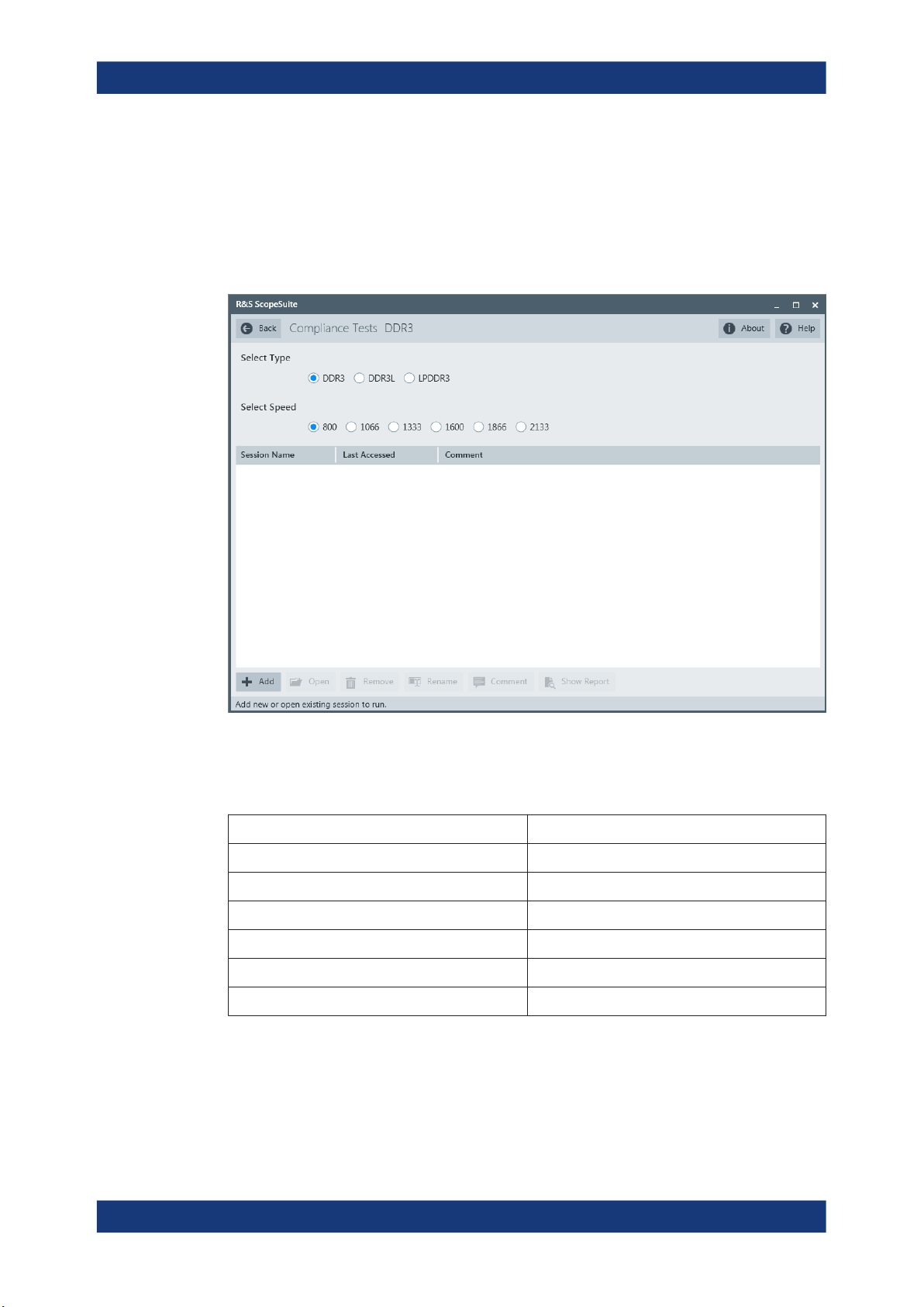
After you open a compliance test, the "Session Selection" dialog appears. In this dialog, you can create new sessions, open or view existing report.
The following functions are available for handling test sessions:
Function Description
"Add" Adds a new session
"Open" Opens the selected session
"Remove" Removes the selected session
"Rename" Changes the "Session Name"
"Comment" Adds a comment
"Show report" Generates a report for the selected session
To add a test session
1. In the R&S ScopeSuite window, select the compliance test.
2. In the "Session Selection" dialog press "Add".
3. If necessary change the "Session Name"
14User Manual 1178.8771.02 ─ 07

R&S®RTO-K91, R&S®RTO6-K91, R&S®RTP-K91
To open a test session
1. In the R&S ScopeSuite window, select the compliance test.
2. In the "Session Selection" dialog, select the session you want to open and double
click on it.
Alternatively, select the session and press "Open".
To show a report for a test session
1. In the R&S ScopeSuite window, select the compliance test.
2. In the "Session Selection" dialog, select the session you want the report for and
press "Show report".
3.2 Configuring the Test
Performing Tests
Configuring the Test
1. In the R&S ScopeSuite window, select the compliance test to be performed:
● "DDR3"
2. Open a test session, see Chapter 3.1, "Starting a Test Session", on page 14.
3. Adjust the "Properties" settings for the test cases you want to perform.
4. Click "Limit Manager" and edit the limit criteria, see Chapter 3.2.1.1, "Limit Man-
ager", on page 17.
5. If you want to use special report settings the "Report Config" tab to define the format and contents of the report. Otherwise the settings defined in "RSScopeSuite" >
"Settings" > "Report" are used. See Chapter 2.6, "Report Configuration",
on page 13.
6. Click "Test Checked"/"Test Single" and proceed as described in the relevant test
case chapter.
15User Manual 1178.8771.02 ─ 07

R&S®RTO-K91, R&S®RTO6-K91, R&S®RTP-K91
3.2.1 General Test Settings
Performing Tests
Configuring the Test
Each session dialog is divided into several sections:
●
"Properties": shows the settings that can be made for the test case selected on the
left side of the dialog. You can differentiate between the "All" and the sub test properties
In the "All" > "Properties" tab you can configure the settings for all test cases in the
current session. Once you change and save a setting in this tab, the changes will
be done for all test in the sessions. At the same time, there will be a special marking for the functions that have different settings for different sub tests.
●
"Limit Manager": sets the measurement limits that are used for compliance testing,
see Chapter 3.2.1.1, "Limit Manager", on page 17.
●
"Results": shows an overview of the available test results for this session.
●
"Instruments": defines instruments settings for connecting to external devices, that
are specific for this test session.
When a session is first created the global settings ("RSScopeSuite" > "Settings" >
"Instruments") are copied to the session. This "Instruments" tab can be used to
change those copied defaults.
●
"Report Config": defines the format and contents of the report for this session.
16User Manual 1178.8771.02 ─ 07

R&S®RTO-K91, R&S®RTO6-K91, R&S®RTP-K91
When a session is first created the global settings ("RSScopeSuite" > "Settings" >
"Report") are copied to the session. This "Report Config" tab can be used to
change those copied defaults.
●
"Test Checked"/ "Test Single": starts the selected test group.
3.2.1.1 Limit Manager
The "Limit Manager" shows the measurement limits that are used for compliance testing.
Each limit comprises the comparison criterion, the unit, the limit value A, and a second
limit value B if the criterion requires two limits.
You can set the values to defaults, change the values in the table, export the table in
xml format, or import xml files with limit settings.
► Check and adjust the measurement limits.
Performing Tests
Configuring the Test
17User Manual 1178.8771.02 ─ 07

R&S®RTO-K91, R&S®RTO6-K91, R&S®RTP-K91
Performing Tests
Configuring the Test
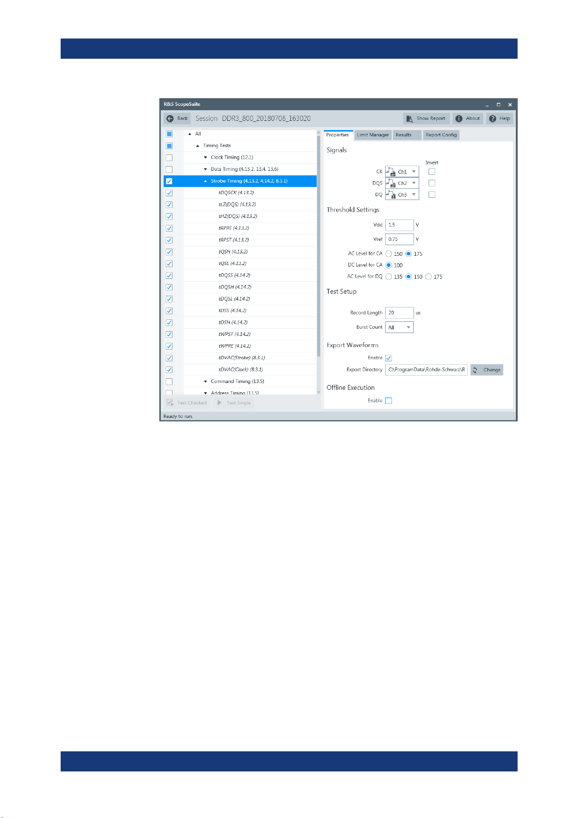
3.2.2 Test Configuration for DDR3
The test configuration consists of some test-specific configuration settings. The values
for the settings in this tab depend on the selected "Speed" and "Type" of standard.
18User Manual 1178.8771.02 ─ 07

R&S®RTO-K91, R&S®RTO6-K91, R&S®RTP-K91
Performing Tests
Configuring the Test
Figure 3-1: Configuration for DDR3 compliance tests
Signals
Selects the channel for the specified signal.
For electrical tests consider also how many test signals are enabled. For example, if
only the ADD/CMD signal is selected, only ADD/CMD signal is used to run the test. If
both the ADD and the CMD signals are selected, test is run using ADD signal first, followed by the CMD signal.
The following signals are available according to the selected test case:
"ADD"
"CMD"
"CK"
"DQS"
"DQ"
"DM"
"CS"
"CKE"
Address signal.
Command signal.
Differential clock input signal.
Data strobe signal.
Data input/output signal.
Data mask signal.
Chip select signal.
Clock enable signal.
19User Manual 1178.8771.02 ─ 07

R&S®RTO-K91, R&S®RTO6-K91, R&S®RTP-K91
Threshold Settings
The following threshold settings are defined:
"VDD"
Power Supply: 1.5 V +/- 0.075 V
Performing Tests
Configuring the Test
"V
"
REF
"VSS"
"V
"
DDQ
"VTT"
"V
"
SSQ
"AC Level for
Reference voltage
Ground
DQ Power Supply: 1.5 V +/- 0.075 V
VTT = V
DDQ
/2
DQ Ground
AC level for the command address.
CA"
"DC Level for
DC level for the command address.
CA"
"AC Level for
AC level for the data input/output signal.
DQ"
"DC Level for
DC level for the data input/output signal.
DQ"
Average Window
Sets the average window in periods.
Record Length
Sets the number of waveform samples in one waveform record.
Burst Count
Sets the burst count.
Speed Bin
Selects which speed bin is used for the tests.
CAS Latency (CL)
Selects the value for the CAS latency. This is the delay, measured in clock cycles,
between the internal read command and the availability of the first bit of output data.
CAS Write Latency (CWL)
Selects the value for the CAS write latency. This is the delay, measured in clock cycles,
between the internal write command and the availability of the first bit input data.
Export Waveforms
Enables you to export a waveform. You can later load the waveforms to run the tests in
the offline mode, see Offline Execution.
You can define an export directory, or use the default one:
MyDocuments\Rohde-Schwarz\RSScopeSuite\<Version>\Waveforms\
<ComplianceTest>\<SubTest>\<Speed>\<SessionName>
For example:
20User Manual 1178.8771.02 ─ 07

R&S®RTO-K91, R&S®RTO6-K91, R&S®RTP-K91
MyDocuments\Rohde-Schwarz\RSScopeSuite\4.10.0\Waveforms\DDR3\
DDR3\1333\DDR3_1333_20180413_144116
Offline Execution
Performing Tests
Initiating the Test
If enabled, allows you to use exported waveforms as a source for the execution of the
compliance test.
You can select one waveform for each needed signal.
3.3 Initiating the Test
To perform compliance tests, the device under test is connected to the test board in a
test-specific way. Using a probe, the test board is connected with the R&S RTO/RTO6/
RTP. The probe connections are test-specific. The R&S ScopeSuite guides you stepby-step through the connection setup and the test sequence.
1. Set the test setup on a nonconductive, static-approved work surface.
2. In the R&S ScopeSuite window, select the compliance test.
3. Open a test session, see Chapter 3.1, "Starting a Test Session", on page 14.
21User Manual 1178.8771.02 ─ 07

R&S®RTO-K91, R&S®RTO6-K91, R&S®RTP-K91
4. Check the test configuration settings and adjust, if necessary. See: Chapter 3.2,
"Configuring the Test", on page 15.
5. Click "Test Checked" for starting all checked test cases or "Test Single" for starting
only the selected test case.
The R&S ScopeSuite test wizard explains the following individual setup steps. A
detailed test description can be found in the following chapters:
● Chapter 3.5, "Starting DDR3 Tests", on page 23
3.4 Getting Test Results
For each test, the test data - report, diagrams and waveform files - is saved in the following folder:
%ProgramData%\Rohde-Schwarz\RSScopeSuite2\<version>\Sessions\DDR3\
<Session_Name>
Performing Tests
Getting Test Results
If you resume an existing session, new measurements are appended to the report,
new diagrams and waveform files are added to the session folder. Existing files are not
deleted or replaced. Sessions data remain until you delete them in the "Results" tab of
the session.
The report format can be defined in "RSScopeSuite" > "Settings" > "Report" for all
compliance tests (see also Chapter 2.6, "Report Configuration", on page 13). If you
want to use special report settings for a session, you can define the format and contents of the report in the "Report Config" tab of the session.
All test results are listed in the "Results" tab. Reports can be provided in PDF,
MSWord, or HTML format. To view and print PDF reports, you need a PDF viewer, for
example, the Acrobat Reader.
The test report file can be created at the end of the test, or later in the "Session Selection" dialog.
To show a test report
1. In the R&S ScopeSuite window, select the compliance test to be performed.
2. Select the session name in the "Session Selection" dialog and click "Show report".
The report opens in a separate application window, depending on the file format.
You can check the test results and print the report.
To delete the results, diagrams and waveform files of a session
1. In the "Session Selection" dialog select the session and open it.
2. In the "Results" tab, select the result to be deleted.
3. Click "Remove".
22User Manual 1178.8771.02 ─ 07

R&S®RTO-K91, R&S®RTO6-K91, R&S®RTP-K91
3.5 Starting DDR3 Tests
Before you run the test, complete the following actions:
●
LAN connection of the oscilloscope and the computer running the R&S ScopeSuite, see Chapter 2.5, "Connecting the R&S RTO/RTO6/RTP", on page 11
1. Select "DDR3" in the R&S ScopeSuite start window.
2. In the "Session Selection" dialog, set the "Select Type" standard. The following
"Types" are available:
● "DDR3": Double data rate type three. Used for desktops and servers.
● "DDR3L": DDR3 low voltage. It is used in laptops and low power PCs.
● "LPDDR3": low power DDR3. Consumes very low power and is used for mobile
phones.
3. Set the "Select Speed". There are preset speeds you can select from:
"800"/"1066"/"1333"/"1600"/"1866"/"2133"
Performing Tests
Starting DDR3 Tests
4. Add a new test session. Open it, see Chapter 3.1, "Starting a Test Session",
on page 14.
5. Check the test configuration settings. Adjust, if necessary. See:
● Chapter 3.2.2, "Test Configuration for DDR3", on page 18
● Chapter 3.2.1.1, "Limit Manager", on page 17
6. Select/check the test cases you want to run and click "Test Single"/"Test checked".
7. A step-by step guide explains the following individual setup steps. When you have
finished all steps of the step-by-step guide, the compliance test runs automatically.
23User Manual 1178.8771.02 ─ 07
R&S®RTO-K91, R&S®RTO6-K91, R&S®RTP-K91
4 Timing Tests
4.1 Clock Timing
4.1.1 Test Equipment
Item Description, model Quantity
Timing Tests
Clock Timing
Rohde & Schwarz oscilloscope R&S RTP with 4 channels and minimum 8 GHz band-
Modular Probe Probe with minimum 9 GHz bandwidth 1
Probe tip R&S RT-ZMA10 1
DUT DDR3 device that supports the selected type 1
4.1.2 Performing the Tests
1. Start the test as described in Chapter 3.5, "Starting DDR3 Tests", on page 23.
2. Select "Timing Tests" > "Clock Timing".
1
width
R&S RTO2000/RTO6 with 4 channels and minimum 4
GHz bandwidth
24User Manual 1178.8771.02 ─ 07

R&S®RTO-K91, R&S®RTO6-K91, R&S®RTP-K91
Timing Tests
Clock Timing
3. Enable the tests that you want to run.
4. Click "Test Single".
5. Follow the instructions of the step-by step guide.
When you have finished all steps, the compliance test runs automatically.
6. You can also run the test in offline mode, using downloaded waveforms. For
details, see Chapter 3.2.2, "Test Configuration for DDR3", on page 18.
4.1.3 Test Setup
The software guides you to make the proper connections. Follow the steps to conduct
the test.
The software is intended to facilitate the execution of a set of measurements on the relevant signals.
Consider also the soldering guide, see Chapter 2.1.1, "Soldering Guide for Modular
Probes", on page 9.
4.1.4 Measurements
The clock timing measurements consist of up to eight measurements. They test the
limits as defined in the JESD79-3F(DDR3)/JESD79-3-1A-01(DDR3L)/
JESD209-3C(LPDDR3) specifications.
25User Manual 1178.8771.02 ─ 07

R&S®RTO-K91, R&S®RTO6-K91, R&S®RTP-K91
Timing Tests
Clock Timing
4.1.4.1 Average Clock Period - t
CK(avg)
This test aims to verify that the average clock period tCK(avg) is within the limits
defined in section 12.1.1 (DDR3/DDR3L)/ 11.1.1 (LPDDR3) of the specification. This is
the average clock period calculated across any consecutive 200 cycle window. The
clock period is defined from rising edge to rising edge.
4.1.4.2 Absolute Clock Period - t
CK(abs)
This test aims to verify that the average absolute clock period tCK(abs) is within the
limits defined in section 12.1.2 (DDR3/DDR3L)/ 11.1.2 (LPDDR3) of the specification.
This is the absolute clock period from one rising edge to the next rising edge.
4.1.4.3 Average Low Pulse Width - t
This test aims to verify that the average low pulse width tCL(avg) is within the limits
defined in section 12.1.3 (DDR3/DDR3L)/ 11.1.3 (LPDDR3) of the specification. This is
the average low pulse width, as calculated across any consecutive 200 low pulses.
4.1.4.4 Average High Pulse Width - t
CL(avg)
CH(avg)
This test aims to verify that the average high pulse width tCL(avg) is within the limits
defined in section 12.1.3 (DDR3/DDR3L)/ 11.1.3 (LPDDR3) of the specification. This is
the average low pulse width, as calculated across any consecutive 200 low pulses.
4.1.4.5 Clock Period Jitter - t
JIT(per)
This test aims to verify that the clock period jitter tJIT(per) is within the limits defined in
section 12.1.4 (DDR3/DDR3L)/ 11.1.4 (LPDDR3) of the specification. It is the largest
deviation of any signal tCK from tCK(avg). It defines the single period jitter when the
DLL is already locked.
4.1.4.6 Half Period Jitter - t
JIT(duty)
This test aims to verify that the half period jitter tJIT(duty) is within the limits defined in
section 12.1.4 (DDR3/DDR3L)/ 11.1.4 (LPDDR3) of the specification. This is the largest deviation of any signal tCK from t
4.1.4.7 Cycle to Cycle Period Jitter - t
This test aims to verify that the cycle to cycle period jitter tJIT(cc) is within the limits
defined in section 12.1.5 (DDR3/DDR3L)/ 11.1.5 (LPDDR3) of the specification. This is
the absolute difference in clock period between two consecutive clock cycles. It defines
the cycle to cycle jitter when the DLL is already locked.
JIT(cc)
CK(avg)
.
26User Manual 1178.8771.02 ─ 07
R&S®RTO-K91, R&S®RTO6-K91, R&S®RTP-K91
Timing Tests
Data Timing
4.1.4.8 Cumulative Error - t
This test aims to verify that the cumulative error tERR(nper) is within the limits defined
in section 12.1.6 (DDR3/DDR3L)/ 11.1.6 (LPDDR3) of the specification. This is the
cumulative error across n multiple consecutive cycles from tCK(avg).
4.2 Data Timing
4.2.1 Test Equipment
Item Description, model Quantity
Rohde & Schwarz oscilloscope R&S RTP with 4 channels and minimum 8 GHz band-
Modular Probe Probe with minimum 9 GHz bandwidth 3
Probe tip R&S RT-ZMA10 3
ERR(nper)
1
width
R&S RTO2000/RTO6 with 4 channels and minimum 4
GHz bandwidth
DUT DDR3 device that supports the selected type 1
4.2.2 Performing the Tests
1. Start the test as described in Chapter 3.5, "Starting DDR3 Tests", on page 23.
2. Select "Timing Tests" > "Data Timing".
27User Manual 1178.8771.02 ─ 07

R&S®RTO-K91, R&S®RTO6-K91, R&S®RTP-K91
Timing Tests
Data Timing
3. Enable the tests that you want to run.
4. Click "Test Single".
5. Follow the instructions of the step-by step guide.
When you have finished all steps, the compliance test runs automatically.
6. You can also run the test in offline mode, using downloaded waveforms. For
details, see Chapter 3.2.2, "Test Configuration for DDR3", on page 18.
4.2.3 Test Setup
The software guides you to make the proper connections. Follow the steps to conduct
the test.
The software is intended to facilitate the execution of a set of measurements on the relevant signals.
Consider also the soldering guide, see Chapter 2.1.1, "Soldering Guide for Modular
Probes", on page 9.
28User Manual 1178.8771.02 ─ 07

R&S®RTO-K91, R&S®RTO6-K91, R&S®RTP-K91
4.2.4 Measurements
The data timing measurements consist of up to ten measurements. They test the limits
as defined in the JESD79-3F(DDR3)/JESD79-3-1A-01(DDR3L)/
JESD209-3C(LPDDR3) specifications.
Timing Tests
Data Timing
4.2.4.1 Differential DQ and DM Input Setup Time- t
DS(base)
This test aims to verify that time interval from the data or data mask (DQ/DM rising/
falling edge) setup time to the associated DQS crossing edge is within the limits
defined in section 13.6 of the specification.
4.2.4.2 Differential DQ and DM Input Hold Time - t
DH(base)
This test aims to verify that the time interval from the data or data mask (DQ/DM rising/
falling edge) hold time to the associated DQS crossing edge is within the limits defined
in section 13.6 of the specification.
4.2.4.3 Differential DQ and DM Input Setup Time with Derating Support - t
This test aims to verify that the time interval from data or data mask (DQ/DM rising/
falling edge) setup time to the associated DQS crossing is within the limits defined in
section 13.6 of the specification.
4.2.4.4 Differential DQ and DM Input Hold Time with Derating Support - t
This test aims to verify that the time interval from data or data mask (DQ/DM rising/
falling edge) hold time to the associated DQS crossing is within the limits defined in
section 13.6 of the specification..
DS-Diff(derate)
DH-Diff(derate)
4.2.4.5 DQ Out High Impedance Time From CK/CK# - t
This test aims to verify that the data high impedance time from CK/CK# is within the
limits defined in section 4.13.2 of the specification.
4.2.4.6 DQ Low-Impedance Time from CK/CK# - t
LZ(DQ)
This test aims to verify that the data low impedance time from CK/CK# is within the limits defined in section 4.13.2 of the specification.
4.2.4.7 Data Input Pulse Width - t
DIPW
This test aims to verify that the data and mask input pulse width for each input is within
the limits defined in section 13.4 Note 28 of the specification.
HZ(DQ)
29User Manual 1178.8771.02 ─ 07
R&S®RTO-K91, R&S®RTO6-K91, R&S®RTP-K91
Timing Tests
Strobe Timing
4.2.4.8 DQS-DQ Skew for DQS and Associated DQ Signals - t
This test aims to verify that the strobe to data skew, per group, per access is within the
limits defined in section 4.13.2 of the specification.
4.2.4.9 DQ/DQS Output Hold Time From DQS - t
QH
This test aims to verify that the data output hold time from strobe is within the limits
defined in section 4.13.2 of the specification.
4.2.4.10 t
Time above V
VAC
This test aims to verify that t
IH(ac) VIL(ac)
is within the limits defined in the specification. This is
VAC
the time to remain above/below V
IH(AC)/VIL(AC)
for a data transition to be considered as
valid.
4.3 Strobe Timing
DQSQ
4.3.1 Test Equipment
Item Description, model Quantity
Rohde & Schwarz oscilloscope R&S RTP with 4 channels and minimum 8 GHz band-
Modular Probe Probe with minimum 9 GHz bandwidth 3
Probe tip R&S RT-ZMA10 3
DUT DDR3 device that supports the selected type 1
4.3.2 Performing the Tests
1. Start the test as described in Chapter 3.5, "Starting DDR3 Tests", on page 23.
2. Select "Timing Tests" > "Strobe Timing".
1
width
R&S RTO2000/RTO6 with 4 channels and minimum 4
GHz bandwidth
30User Manual 1178.8771.02 ─ 07
R&S®RTO-K91, R&S®RTO6-K91, R&S®RTP-K91
Timing Tests
Strobe Timing
3. Enable the tests that you want to run.
4. Click "Test Single".
5. Follow the instructions of the step-by step guide.
When you have finished all steps, the compliance test runs automatically.
6. You can also run the test in offline mode, using downloaded waveforms. For
details, see Chapter 3.2.2, "Test Configuration for DDR3", on page 18.
4.3.3 Test Setup
The software guides you to make the proper connections. Follow the steps to conduct
the test.
The software is intended to facilitate the execution of a set of measurements on the relevant signals.
Consider also the soldering guide, see Chapter 2.1.1, "Soldering Guide for Modular
Probes", on page 9.
31User Manual 1178.8771.02 ─ 07

R&S®RTO-K91, R&S®RTO6-K91, R&S®RTP-K91
4.3.4 Measurements
The strobe measurements consist of up to ten measurements. They test the limits as
defined in the JESD79-3F(DDR3)/JESD79-3-1A-01(DDR3L)/JESD209-3C(LPDDR3)
specifications.
Timing Tests
Strobe Timing
4.3.4.1 DQS Output Access Time from CK/CK # - t
This test aims to verify that the strobe rising edge output access time from rising
CK/CK# is within the limits defined in section 4.13.2 of the specification.
4.3.4.2 Low-Impedance Time from CK/CK# - t
LZ
This test aims to verify that the strobe low-impedance time is within the limits defined in
section 4.13.2 of the specification.
4.3.4.3 High-Impedance Time from CK/CK# - t
HZ
This test aims to verify that the strobe high-impedance time is within the limits defined
in section 4.13.2 of the specification.
4.3.4.4 Differential Read Preamble - t
RPRE
This test aims to verify that the strobe differential READ Preamble is within the limits
defined in section 4.13.2 of the specification.
4.3.4.5 Read Postamble - t
RPST
DQSCK
This test aims to verify that the strobe differential READ Postamble is within the limits
defined in section 4.13.2 of the specification.
4.3.4.6 Differential Output High Time - t
QSH
This test aims to verify that the strobe differential output high time is within the limits
defined in section 4.13.2 of the specification.
4.3.4.7 Differential Output Low Time - t
QSL
This test aims to verify that the strobe differential output low time is within the limits
defined in section 4.13.2 of the specification.
4.3.4.8 DQS Latching Transition to Associated Clock Edge - t
This test aims to verify that the time interval from the strobe rising edge to CK/CK# rising edge is within the limits defined in section 4.14.2 of the specification.
DQSS
32User Manual 1178.8771.02 ─ 07

R&S®RTO-K91, R&S®RTO6-K91, R&S®RTP-K91
Timing Tests
Strobe Timing
4.3.4.9 DQS Input High Pulse Width - t
DQSH
This test aims to verify that the strobe differential input high pulse width is within the
limits defined in section 4.14.2 of the specification.
4.3.4.10 DQS Input Low Pulse Width - t
DQSL
This test aims to verify that the strobe differential input low pulse width is within the limits defined in section 4.14.2 of the specification.
4.3.4.11 DQS Falling Edge to CK Setup Time - t
This test aims to verify that the time interval from the strobe falling edge setup time to
the CK/CK# rising edge is within the limits defined in section 4.14.2 of the specification.
4.3.4.12 DQS Falling Edge Hold Time from CK - t
This test aims to verify that the strobe falling edge hold time from CK/CK# rising edge
is within the limits defined in section 4.14.2 of the specification.
4.3.4.13 Write Postamble - t
WPST
DSS
DSH
This test aims to verify that the strobe differential WRITE Postamble is within the limits
defined in section 4.14.2 of the specification.
4.3.4.14 Write Preamble - t
WPRE
This test aims to verify that the strobe differential WRITE Preamble is within the limits
defined in section 4.14.2 of the specification.
4.3.4.15 Time before Ringback - t
This test aims to verify that the time before ringback for strobe is within the limits
defined in section 8.3.1 of the specification. This is the "time above AC-level" during a
differential AC-swing.
4.3.4.16 Time before Ringback - t
This test aims to verify that the time before ringback for CK /CK# is within the limits
defined in section 8.3.1 of the specification. This is the "time above AC-level" during a
differential AC-swing.
DVAC(Strobe)
DVAC(Clock)
33User Manual 1178.8771.02 ─ 07

R&S®RTO-K91, R&S®RTO6-K91, R&S®RTP-K91
4.4 Command Timing
4.4.1 Test Equipment
Item Description, model Quantity
Timing Tests
Command Timing
Rohde & Schwarz oscilloscope R&S RTP with 4 channels and minimum 8 GHz band-
Modular Probe Probe with minimum 9 GHz bandwidth 2
Probe tip R&S RT-ZMA10 2
DUT DDR3 device that supports the selected type 1
4.4.2 Performing the Tests
1. Start the test as described in Chapter 3.5, "Starting DDR3 Tests", on page 23.
2. Select "Timing Tests" > "Command Timing".
1
width
R&S RTO2000/RTO6 with 4 channels and minimum 4
GHz bandwidth
34User Manual 1178.8771.02 ─ 07

R&S®RTO-K91, R&S®RTO6-K91, R&S®RTP-K91
Timing Tests
Command Timing
3. Enable the tests that you want to run.
4. Click "Test Single".
5. Follow the instructions of the step-by step guide.
When you have finished all steps, the compliance test runs automatically.
6. You can also run the test in offline mode, using downloaded waveforms. For
details, see Chapter 3.2.2, "Test Configuration for DDR3", on page 18.
4.4.3 Test Setup
The software guides you to make the proper connections. Follow the steps to conduct
the test.
The software is intended to facilitate the execution of a set of measurements on the relevant signals.
Consider also the soldering guide, see Chapter 2.1.1, "Soldering Guide for Modular
Probes", on page 9.
35User Manual 1178.8771.02 ─ 07

R&S®RTO-K91, R&S®RTO6-K91, R&S®RTP-K91
4.4.4 Measurements
The command timing measurements consist of up to six measurements. They test the
limits as defined in section 13.5 (DDR3/DDR3L)/ 4.2 (LPDDR3) of the
JESD79-3F(DDR3)/JESD79-3-1A-01(DDR3L)/JESD209-3C(LPDDR3) specifications.
Timing Tests
Command Timing
4.4.4.1 Address and Control Input Setup Time - t
IS
This test aims to verify that the command and address setup time from CK/CK# is
within the limits defined in the specification.
4.4.4.2 Address and Control Input Setup Time with Derating Support - t
This test aims to verify that the command and address setup time from CK/CK# is
within the limits defined in the specification.
4.4.4.3 Address and Control Input Hold Time - t
IH
This test aims to verify that the command and address hold time from CK/CK# is within
the limits defined in the specification.
4.4.4.4 Address and Control Input Hold Time with Derating Support - t
This test aims to verify that the command and address hold time from CK/CK# is within
the limits defined in the specification.
4.4.4.5 Address and Control Input Pulse Width t
IPW
IS (Derated)
IH (Derated)
4.4.4.6 t
This test aims to verify that the control and address input pulse width for each input is
within the limits defined in the specification.
VAC (CA)
This test aims to verify that t
is the time to remain above/below V
is within the limits defined in the specification. This
VAC (CA)
IH(AC)/VIL(AC)
for a command transition to be consid-
ered as valid.
36User Manual 1178.8771.02 ─ 07
R&S®RTO-K91, R&S®RTO6-K91, R&S®RTP-K91
4.5 Address Timing
4.5.1 Test Equipment
Item Description, model Quantity
Timing Tests
Address Timing
Rohde & Schwarz oscilloscope R&S RTP with 4 channels and minimum 8 GHz band-
Modular Probe Probe with minimum 9 GHz bandwidth 2
Probe tip R&S RT-ZMA10 2
DUT DDR3 device that supports the selected type 1
4.5.2 Performing the Tests
1. Start the test as described in Chapter 3.5, "Starting DDR3 Tests", on page 23.
2. Select "Timing Tests" > "Address Timing".
1
width
R&S RTO2000/RTO6 with 4 channels and minimum 4
GHz bandwidth
37User Manual 1178.8771.02 ─ 07
R&S®RTO-K91, R&S®RTO6-K91, R&S®RTP-K91
Timing Tests
Address Timing
3. Enable the tests that you want to run.
4. Click "Test Single".
5. Follow the instructions of the step-by step guide.
When you have finished all steps, the compliance test runs automatically.
6. You can also run the test in offline mode, using downloaded waveforms. For
details, see Chapter 3.2.2, "Test Configuration for DDR3", on page 18.
4.5.3 Measurements
The address timing measurements consist of up to six measurements. They test the
limits as defined in section 13.5 (DDR3/DDR3L)/ 4.2 (LPDDR3) of the
JESD79-3F(DDR3)/JESD79-3-1A-01(DDR3L)/JESD209-3C(LPDDR3) specifications.
For details on the measurements, see Chapter 4.4.4, "Measurements", on page 36.
38User Manual 1178.8771.02 ─ 07

R&S®RTO-K91, R&S®RTO6-K91, R&S®RTP-K91
4.6 Chip Select Timing
4.6.1 Test Equipment
Item Description, model Quantity
Timing Tests
Chip Select Timing
Rohde & Schwarz oscilloscope R&S RTP with 4 channels and minimum 8 GHz band-
Modular Probe Probe with minimum 9 GHz bandwidth 2
Probe tip R&S RT-ZMA10 2
DUT DDR3 device that supports the selected type 1
4.6.2 Performing the Tests
1. Start the test as described in Chapter 3.5, "Starting DDR3 Tests", on page 23.
2. Select "Timing Tests" > "Chip Select Timing".
1
width
R&S RTO2000/RTO6 with 4 channels and minimum 4
GHz bandwidth
39User Manual 1178.8771.02 ─ 07

R&S®RTO-K91, R&S®RTO6-K91, R&S®RTP-K91
3. Enable the tests that you want to run.
4. Click "Test Single".
5. Follow the instructions of the step-by step guide.
When you have finished all steps, the compliance test runs automatically.
6. You can also run the test in offline mode, using downloaded waveforms. For
details, see Chapter 3.2.2, "Test Configuration for DDR3", on page 18.
4.6.3 Test Setup
The software guides you to make the proper connections. Follow the steps to conduct
the test.
The software is intended to facilitate the execution of a set of measurements on the relevant signals.
Consider also the soldering guide, see Chapter 2.1.1, "Soldering Guide for Modular
Probes", on page 9.
Timing Tests
Chip Select Timing
4.6.4 Measurements
The chip select timing measurements consist of up to six measurements. They test the
limits as defined in section 13.5 (DDR3/DDR3L)/ 4.2 (LPDDR3) of the
JESD79-3F(DDR3)/JESD79-3-1A-01(DDR3L)/JESD209-3C(LPDDR3) specifications.
4.6.4.1 Address and Control Input Setup Time - t
This test aims to verify that the chip select setup time from CK/CK# is within the limits
defined in the specification.
4.6.4.2 Address and Control Input Setup Time with Derating Support - tIS (Derated)
This test aims to verify that the chip select setup time from CK/CK# is within the limits
defined in the specification.
4.6.4.3 Address and Control Input Hold Time - t
This test aims to verify that the chip select hold time from CK/CK# is within the limits
defined in the specification.
IS
IH
4.6.4.4 Address and Control Input Hold Time with Derating Support - tIH (Derated)
This test aims to verify that the chip select hold time from CK/CK# is within the limits
defined in the specification.
40User Manual 1178.8771.02 ─ 07

R&S®RTO-K91, R&S®RTO6-K91, R&S®RTP-K91
Timing Tests
Clock Enable Timing
4.6.4.5 t
IPW
This test aims to verify that the chip select input pulse width for each input is within the
limits defined in the specification.
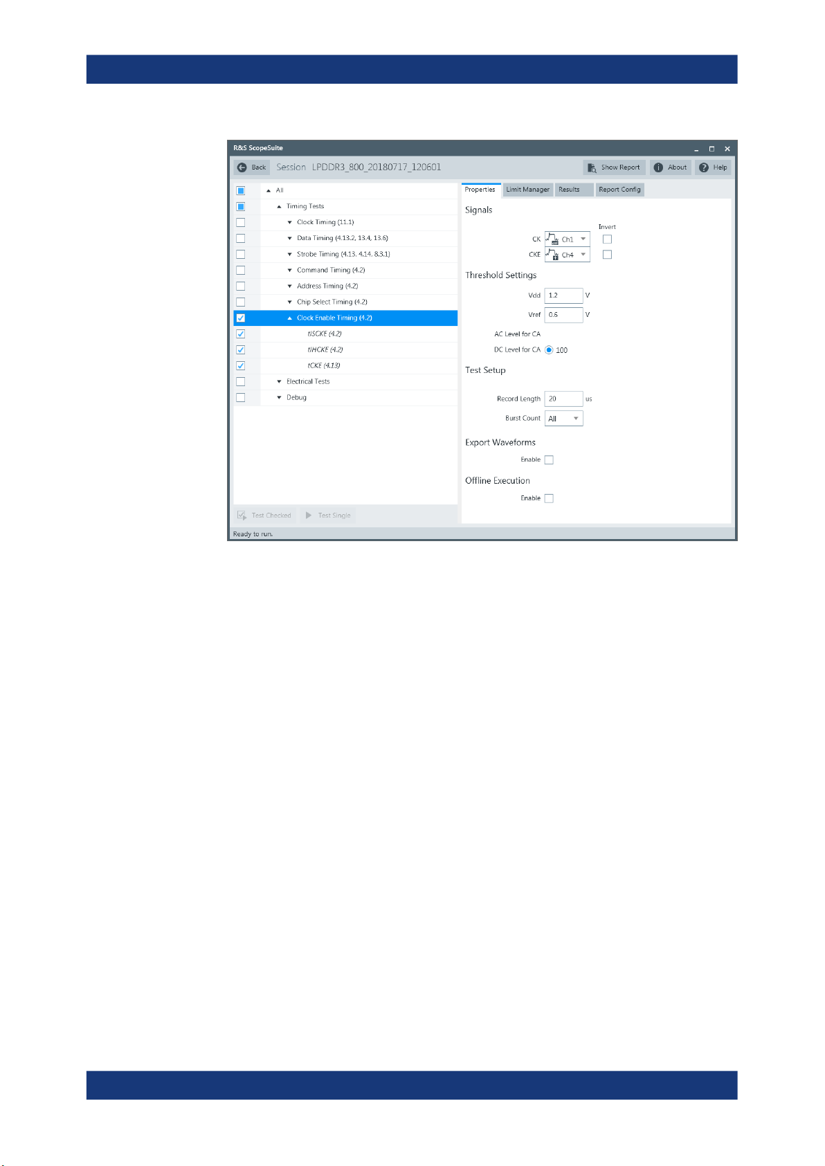
4.7 Clock Enable Timing
4.7.1 Test Equipment
Item Description, model Quantity
Rohde & Schwarz oscilloscope R&S RTP with 4 channels and minimum 8 GHz band-
Modular Probe Probe with minimum 9 GHz bandwidth 2
Probe tip R&S RT-ZMA10 2
DUT DDR3 device that supports the selected type 1
1
width
R&S RTO2000/RTO6 with 4 channels and minimum 4
GHz bandwidth
4.7.2 Performing the Tests
1. Start the test as described in Chapter 3.5, "Starting DDR3 Tests", on page 23.
2. Select "Timing Tests" > "Clock Enable Timing".
41User Manual 1178.8771.02 ─ 07
R&S®RTO-K91, R&S®RTO6-K91, R&S®RTP-K91
Timing Tests
Clock Enable Timing
3. Enable the tests that you want to run.
4. Click "Test Single".
5. Follow the instructions of the step-by step guide.
When you have finished all steps, the compliance test runs automatically.
6. You can also run the test in offline mode, using downloaded waveforms. For
details, see Chapter 3.2.2, "Test Configuration for DDR3", on page 18.
4.7.3 Test Setup
The software guides you to make the proper connections. Follow the steps to conduct
the test.
The software is intended to facilitate the execution of a set of measurements on the relevant signals.
Consider also the soldering guide, see Chapter 2.1.1, "Soldering Guide for Modular
Probes", on page 9.
4.7.4 Measurements
The clock enable timing measurements consist of up to three measurements. They test
the limits as defined in the JESD209-3C(LPDDR3) specification.
42User Manual 1178.8771.02 ─ 07

R&S®RTO-K91, R&S®RTO6-K91, R&S®RTP-K91
Timing Tests
Clock Enable Timing
4.7.4.1 Clock Enable Input Setup Time - t
ISCKE
This test aims to verify that the clock enable input setup time from CKE is within the
limits defined in section 4.2 of the specification.
4.7.4.2 Clock Enable Input Hold Time - t
IH
This test aims to verify that the clock enable hold time from CKE is within the limits
defined in section 4.2 of the specification.
4.7.4.3 Clock Enable Minimum Pulse Width t
This test aims to verify that the minimum pulse width for each input is within the limits
defined in section 4.13 of the specification.
CKE
43User Manual 1178.8771.02 ─ 07

R&S®RTO-K91, R&S®RTO6-K91, R&S®RTP-K91
5 Electrical Tests
5.1 Single-Ended Signals
5.1.1 Input Slew Rate for ADD and CMD
5.1.1.1 Test Equipment
Item Description, model Quantity
Electrical Tests
Single-Ended Signals
Rohde & Schwarz oscilloscope R&S RTP with 4 channels and minimum 8 GHz band-
Modular Probe Probe with minimum 9 GHz bandwidth 2
Probe tip R&S RT-ZMA10 2
DUT DDR3 device that supports the selected type 1
5.1.1.2 Performing the Tests
1. Start the test as described in Chapter 3.5, "Starting DDR3 Tests", on page 23.
2. Select "Electrical Tests" > "Single-Ended Signals" > "Input Slew Rate for ADD and
CMD".
1
width
R&S RTO2000/RTO6 with 4 channels and minimum 4
GHz bandwidth
44User Manual 1178.8771.02 ─ 07

R&S®RTO-K91, R&S®RTO6-K91, R&S®RTP-K91
Electrical Tests
Single-Ended Signals
3. Enable the "Signals" you want to use.
If only the ADD/CMD signal is selected, only ADD/CMD signal will be used to run
the test.
If both the ADD and the CMD signals are selected, test will be run using ADD signal first, followed by the CMD signal.
4. Enable the tests that you want to run.
5. Click "Test Single".
6. Follow the instructions of the step-by step guide.
When you have finished all steps, the compliance test runs automatically.
7. You can also run the test in offline mode, using downloaded waveforms. For
details, see Chapter 3.2.2, "Test Configuration for DDR3", on page 18.
5.1.1.3 Test Setup
The software guides you to make the proper connections. Follow the steps to conduct
the test.
The software is intended to facilitate the execution of a set of measurements on the relevant signals.
Consider also the soldering guide, see Chapter 2.1.1, "Soldering Guide for Modular
Probes", on page 9.
5.1.1.4 Measurements
The input slew rates for address and command measurements consist of up to four
measurements. It tests the limits as defined in sections 8.5 and 13.5 (DDR3/DDR3L)/
45User Manual 1178.8771.02 ─ 07
R&S®RTO-K91, R&S®RTO6-K91, R&S®RTP-K91
7.6 and 11.5 (LPDDR3) of the JESD79-3F(DDR3)/JESD79-3-1A-01(DDR3L)/
JESD209-3C(LPDDR3) specifications.
Setup Slew Rate Rising - SR(tIS) Rising
This test aims to verify that the setup slew rate for rising signal is within the limits
defined in the specification.
Setup Slew Rate Falling - SR(tIS) Falling
This test aims to verify that the setup slew rate for falling signal is within the limits
defined in the specification.
Hold Slew Rate Rising - SR(tIH) Rising
This test aims to verify that the hold slew rate for rising signal is within the limits
defined in the specification.
Hold Slew Rate Falling - SR(tIH) Falling
This test aims to verify that the hold slew rate for falling signal is within the limits
defined in the specification.
Electrical Tests
Single-Ended Signals
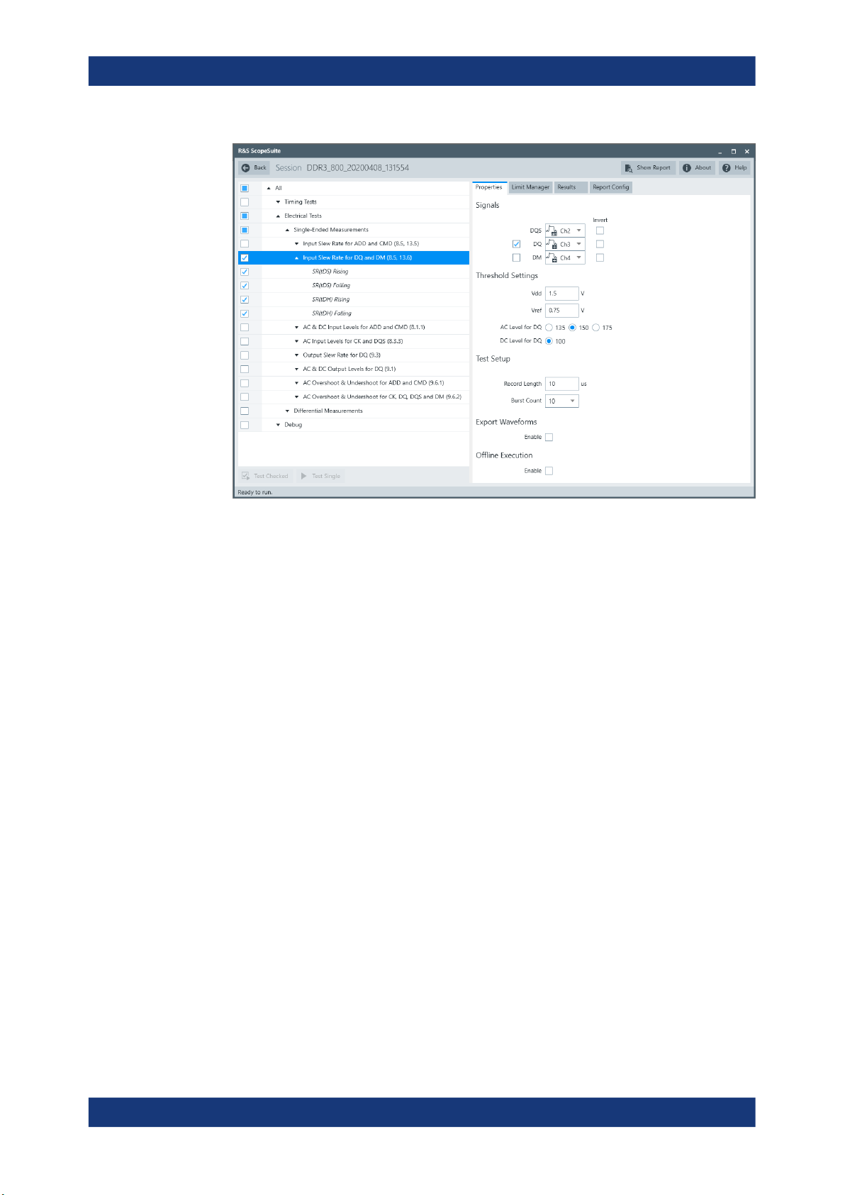
5.1.2 Input Slew Rate for DQ and DM
5.1.2.1 Test Equipment
Item Description, model Quantity
Rohde & Schwarz oscilloscope R&S RTP with 4 channels and minimum 8 GHz band-
width
R&S RTO2000/RTO6 with 4 channels and minimum 4
GHz bandwidth
Modular Probe Probe with minimum 9 GHz bandwidth 2
Probe tip R&S RT-ZMA10 2
DUT DDR3 device that supports the selected type 1
5.1.2.2 Performing the Tests
1. Start the test as described in Chapter 3.5, "Starting DDR3 Tests", on page 23.
2. Select "Electrical Tests" > "Single-Ended Signals" > "Input Slew Rate for DQ and
DM".
1
46User Manual 1178.8771.02 ─ 07
R&S®RTO-K91, R&S®RTO6-K91, R&S®RTP-K91
Electrical Tests
Single-Ended Signals
3. Enable the tests that you want to run.
4. Click "Test Single".
5. Follow the instructions of the step-by step guide.
When you have finished all steps, the compliance test runs automatically.
6. You can also run the test in offline mode, using downloaded waveforms. For
details, see Chapter 3.2.2, "Test Configuration for DDR3", on page 18.
5.1.2.3 Test Setup
The software guides you to make the proper connections. Follow the steps to conduct
the test.
The software is intended to facilitate the execution of a set of measurements on the relevant signals.
Consider also the soldering guide, see Chapter 2.1.1, "Soldering Guide for Modular
Probes", on page 9.
5.1.2.4 Measurements
The input slew rates for data and mask measurements consist of up to four measurements. It tests the limits as defined in sections 8.5 and 13.6 (DDR3/DDR3L)/ 7.6 and
11.6 (LPDDR3) of the JESD79-3F(DDR3)/JESD79-3-1A-01(DDR3L)/
JESD209-3C(LPDDR3) specifications.
47User Manual 1178.8771.02 ─ 07

R&S®RTO-K91, R&S®RTO6-K91, R&S®RTP-K91
Setup Slew Rate Rising - SR(tIS) Rising
This test aims to verify that the setup slew rate for rising signal is within the limits
defined in the specification.
Setup Slew Rate Falling - SR(tIS) Falling
This test aims to verify that the setup slew rate for falling signal is within the limits
defined in the specification.
Hold Slew Rate Rising - SR(tIH) Rising
This test aims to verify that the hold slew rate for rising signal is within the limits
defined in the specification.
Hold Slew Rate Falling - SR(tIH) Falling
This test aims to verify that the hold slew rate for falling signal is within the limits
defined in the specification.
Electrical Tests
Single-Ended Signals
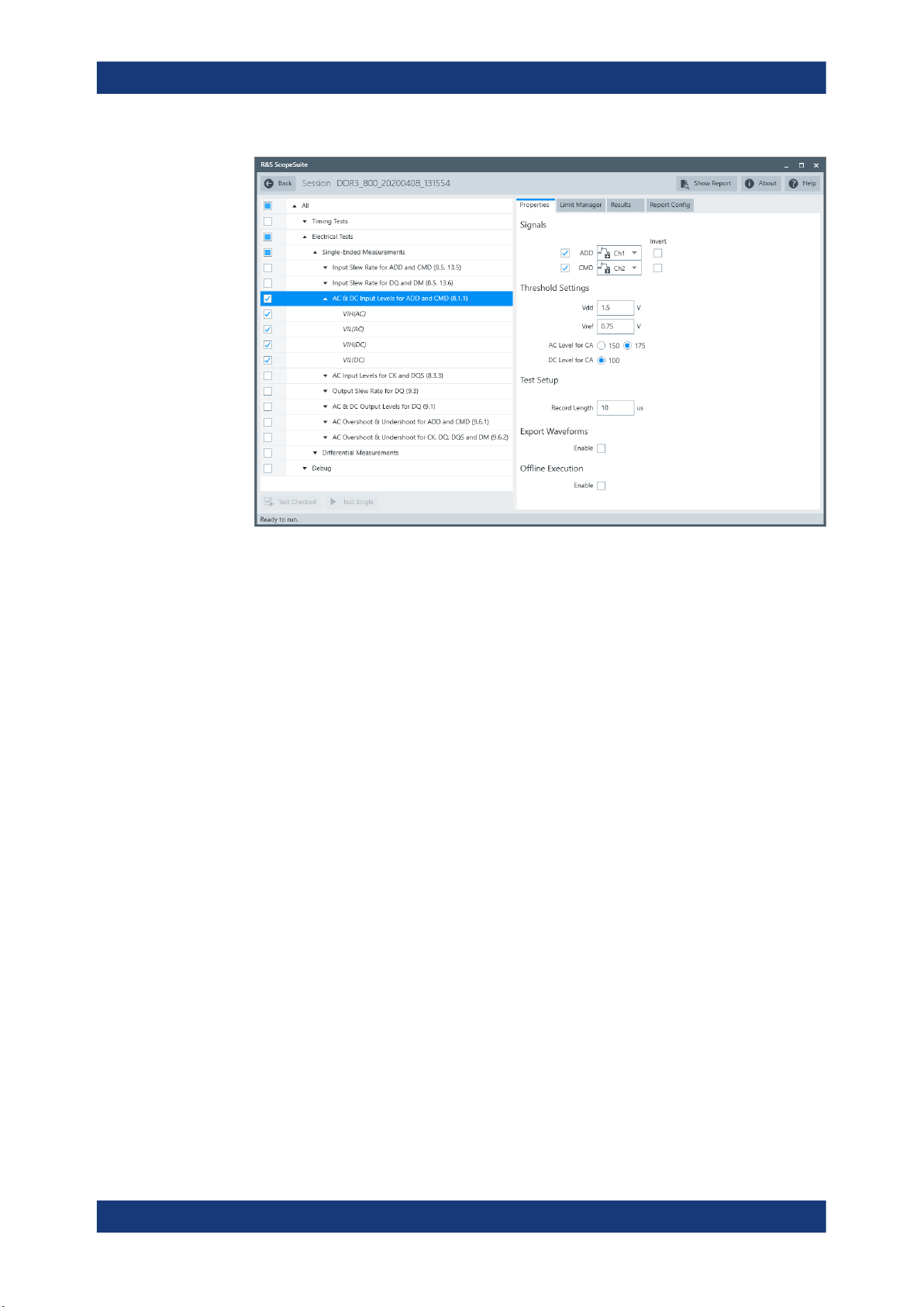
5.1.3 AC & DC Input Levels for ADD and CMD
5.1.3.1 Test Equipment
Item Description, model Quantity
Rohde & Schwarz oscilloscope R&S RTP with 4 channels and minimum 8 GHz band-
width
R&S RTO2000/RTO6 with 4 channels and minimum 4
GHz bandwidth
Modular Probe Probe with minimum 9 GHz bandwidth 2
Probe tip R&S RT-ZMA10 2
DUT DDR3 device that supports the selected type 1
5.1.3.2 Performing the Tests
1. Start the test as described in Chapter 3.5, "Starting DDR3 Tests", on page 23.
2. Select "Electrical Tests" > "Single-Ended Signals" > "AC & DC Input Levels for
ADD and CMD".
1
48User Manual 1178.8771.02 ─ 07
R&S®RTO-K91, R&S®RTO6-K91, R&S®RTP-K91
Electrical Tests
Single-Ended Signals
3. Enable the "Signals" you want to use.
If only the ADD/CMD signal is selected, only ADD/CMD signal will be used to run
the test.
If both the ADD and the CMD signals are selected, test will be run using ADD signal first, followed by the CMD signal.
4. Enable the tests that you want to run.
5. Click "Test Single".
6. Follow the instructions of the step-by step guide.
When you have finished all steps, the compliance test runs automatically.
7. You can also run the test in offline mode, using downloaded waveforms. For
details, see Chapter 3.2.2, "Test Configuration for DDR3", on page 18.
5.1.3.3 Test Setup
The software guides you to make the proper connections. Follow the steps to conduct
the test.
The software is intended to facilitate the execution of a set of measurements on the relevant signals.
Consider also the soldering guide, see Chapter 2.1.1, "Soldering Guide for Modular
Probes", on page 9.
5.1.3.4 Measurements
The AC and DC logic input levels for single-ended address and command measurements consist of up to four measurements. It tests the limits as defined in section
49User Manual 1178.8771.02 ─ 07

R&S®RTO-K91, R&S®RTO6-K91, R&S®RTP-K91
8.1.1(DDR3) / 3.1(DDR3L) / 7.1.1(LPDDR3) of the JESD79-3F(DDR3)/
JESD79-3-1A-01(DDR3L)/JESD209-3C(LPDDR3) specifications.
V
IH(AC)
This test aims to verify that the AC input logic high is within the limits defined in the
specification.
V
IL(AC)
This test aims to verify that the AC input logic low is within the limits defined in the
specification.
V
IH(DC)
This test aims to verify that the DC input logic high is within the limits defined in the
specification.
V
IL(DC)
Electrical Tests
Single-Ended Signals
This test aims to verify that the DC input logic low is within the limits defined in the
specification.
5.1.4 AC Input Levels for CK and DQS
5.1.4.1 Test Equipment
Item Description, model Quantity
Rohde & Schwarz oscilloscope R&S RTP with 4 channels and minimum 8 GHz band-
width
R&S RTO2000/RTO6 with 4 channels and minimum 4
GHz bandwidth
Modular Probe Probe with minimum 9 GHz bandwidth 2
Probe tip R&S RT-ZMA10 2
DUT DDR3 device that supports the selected type 1
5.1.4.2 Performing the Tests
1
1. Start the test as described in Chapter 3.5, "Starting DDR3 Tests", on page 23.
2. Select "Electrical Tests" > "Single-Ended Signals" > "AC Input Levels for CK and
DQS".
50User Manual 1178.8771.02 ─ 07

R&S®RTO-K91, R&S®RTO6-K91, R&S®RTP-K91
Electrical Tests
Single-Ended Signals
3. Enable the tests that you want to run.
4. Click "Test Single".
5. Follow the instructions of the step-by step guide.
When you have finished all steps, the compliance test runs automatically.
6. You can also run the test in offline mode, using downloaded waveforms. For
details, see Chapter 3.2.2, "Test Configuration for DDR3", on page 18.
5.1.4.3 Test Setup
The software guides you to make the proper connections. Follow the steps to conduct
the test.
The software is intended to facilitate the execution of a set of measurements on the relevant signals.
Consider also the soldering guide, see Chapter 2.1.1, "Soldering Guide for Modular
Probes", on page 9.
5.1.4.4 Measurements
The single-ended AC input levels for clock and strobe measurements consist of up to
two measurements. It tests the limits as defined in section 8.3.3 (DDR3) / 7.4.3
(LPDDR3) of the JESD79-3F(DDR3)/JESD209-3C(LPDDR3) specifications.
V
SEH(AC)
This test aims to verify that the single-ended high level for strobes/clock is within the
limits defined in the specification.
51User Manual 1178.8771.02 ─ 07

R&S®RTO-K91, R&S®RTO6-K91, R&S®RTP-K91
V
SEL(AC)
This test aims to verify that the single-ended low level for strobes/clock is within the
limits defined in the specification.
5.1.5 Output Slew Rate for DQ
5.1.5.1 Test Equipment
Item Description, model Quantity
Electrical Tests
Single-Ended Signals
Rohde & Schwarz oscilloscope R&S RTP with 4 channels and minimum 8 GHz band-
Modular Probe Probe with minimum 9 GHz bandwidth 2
Probe tip R&S RT-ZMA10 2
DUT DDR3 device that supports the selected type 1
5.1.5.2 Performing the Tests
1. Start the test as described in Chapter 3.5, "Starting DDR3 Tests", on page 23.
2. Select "Electrical Tests" > "Single-Ended Signals" > "Output Slew Rate for DQ".
1
width
R&S RTO2000/RTO6 with 4 channels and minimum 4
GHz bandwidth
3. Enable the tests that you want to run.
52User Manual 1178.8771.02 ─ 07

R&S®RTO-K91, R&S®RTO6-K91, R&S®RTP-K91
4. Click "Test Single".
5. Follow the instructions of the step-by step guide.
When you have finished all steps, the compliance test runs automatically.
6. You can also run the test in offline mode, using downloaded waveforms. For
details, see Chapter 3.2.2, "Test Configuration for DDR3", on page 18.
5.1.5.3 Test Setup
The software guides you to make the proper connections. Follow the steps to conduct
the test.
The software is intended to facilitate the execution of a set of measurements on the relevant signals.
Consider also the soldering guide, see Chapter 2.1.1, "Soldering Guide for Modular
Probes", on page 9.
Electrical Tests
Single-Ended Signals
5.1.5.4 Measurements
The single-ended output slew rate for data consists of up to two measurements. It tests
the limits as defined in section 9.3 (DDR3) / 8 (DDR3L)/ 8.3 (LPDDR3) of the
JESD79-3F(DDR3)/JESD79-3-1A-01(DDR3L)/JESD209-3C(LPDDR3) specifications.
Slew Rate Query Output Single-Ended Signals Rising- SRQse Rising
This test aims to verify that the single-ended output slew rate for rising edge is within
the limits defined in the specification. It is measured from VOL(AC) to VOH(AC).
Slew Rate Query Output Single-Ended Signals Falling - SRQse Falling
This test aims to verify that the single-ended output slew rate for falling edge is within
the limits defined in the specification. It is measured from VOH(AC) to VOL(AC).
5.1.6 AC & DC Output Levels for DQ
5.1.6.1 Test Equipment
Item Description, model Quantity
Rohde & Schwarz oscilloscope R&S RTP with 4 channels and minimum 8 GHz band-
width
R&S RTO2000/RTO6 with 4 channels and minimum 4
GHz bandwidth
Modular Probe Probe with minimum 9 GHz bandwidth 2
1
53User Manual 1178.8771.02 ─ 07
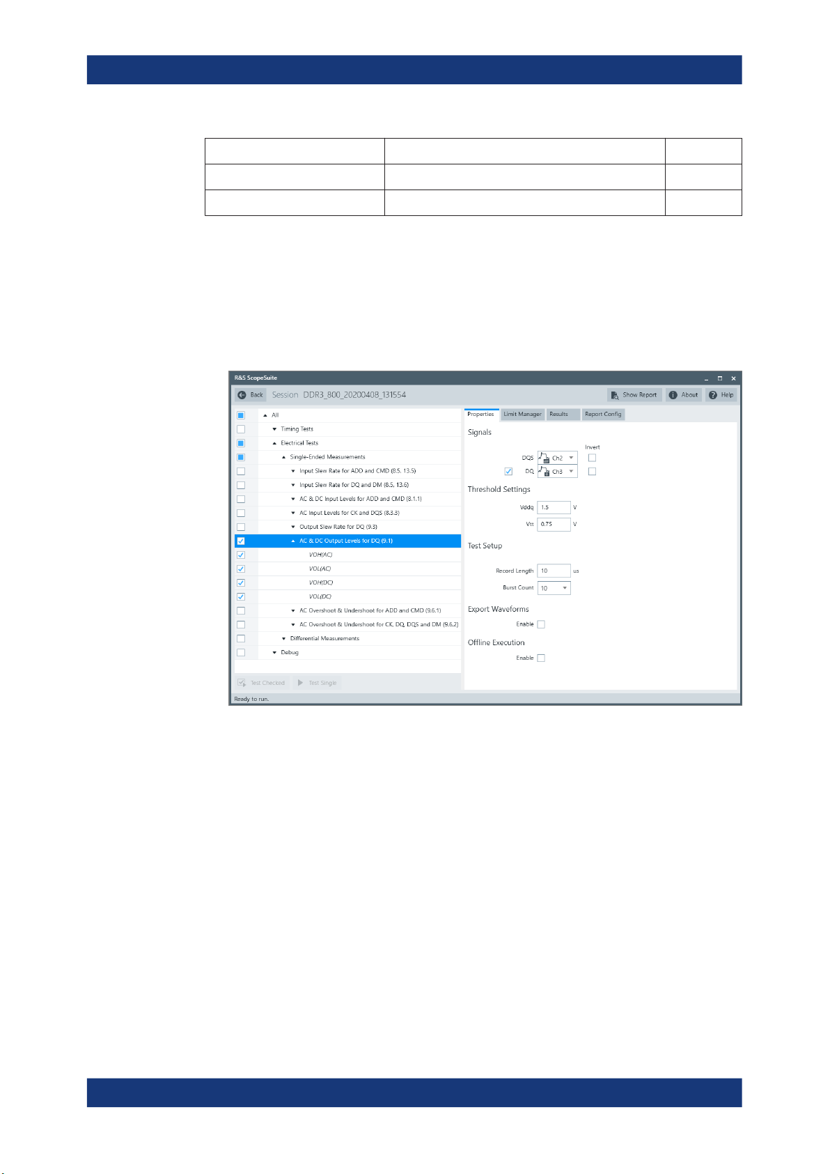
R&S®RTO-K91, R&S®RTO6-K91, R&S®RTP-K91
Item Description, model Quantity
Probe tip R&S RT-ZMA10 2
DUT DDR3 device that supports the selected type 1
5.1.6.2 Performing the Tests
1. Start the test as described in Chapter 3.5, "Starting DDR3 Tests", on page 23.
2. Select "Electrical Tests" > "Single-Ended Signals" > "AC & DC Output Levels for
DQ".
Electrical Tests
Single-Ended Signals
3. Enable the tests that you want to run.
4. Click "Test Single".
5. Follow the instructions of the step-by step guide.
When you have finished all steps, the compliance test runs automatically.
6. You can also run the test in offline mode, using downloaded waveforms. For
details, see Chapter 3.2.2, "Test Configuration for DDR3", on page 18.
5.1.6.3 Test Setup
The software guides you to make the proper connections. Follow the steps to conduct
the test.
The software is intended to facilitate the execution of a set of measurements on the relevant signals.
54User Manual 1178.8771.02 ─ 07

R&S®RTO-K91, R&S®RTO6-K91, R&S®RTP-K91
Consider also the soldering guide, see Chapter 2.1.1, "Soldering Guide for Modular
Probes", on page 9.
5.1.6.4 Measurements
The AC & DC output levels for data measurements consist of up to four measurements. It tests the limits as defined in section 9.1 (DDR3/DDR3L)/ 8.1(LPDDR3) of the
JESD79-3F(DDR3)/JESD79-3-1A-01(DDR3L)/JESD209-3C(LPDDR3) specifications.
V
OH(AC)
This test aims to verify that the AC output high measurement level for the output slew
rate is within the limits defined in the specification.
V
OL(AC)
This test aims to verify that the AC output low measurement level for the output slew
rate is within the limits defined in the specification.
Electrical Tests
Single-Ended Signals
V
OH(DC)
This test aims to verify that the DC output high measurement level for IV curve linearity
is within the limits defined in the specification.
V
OL(DC)
This test aims to verify that the DC output low measurement level for IV curve linearity
is within the limits defined in the specification.
5.1.7 AC Overshoot & Undershoot for ADD and CMD
5.1.7.1 Test Equipment
Item Description, model Quantity
Rohde & Schwarz oscilloscope R&S RTP with 4 channels and minimum 8 GHz band-
width
R&S RTO2000/RTO6 with 4 channels and minimum 4
GHz bandwidth
Modular Probe Probe with minimum 9 GHz bandwidth 2
1
Probe tip R&S RT-ZMA10 2
DUT DDR3 device that supports the selected type 1
5.1.7.2 Performing the Tests
1. Start the test as described in Chapter 3.5, "Starting DDR3 Tests", on page 23.
55User Manual 1178.8771.02 ─ 07
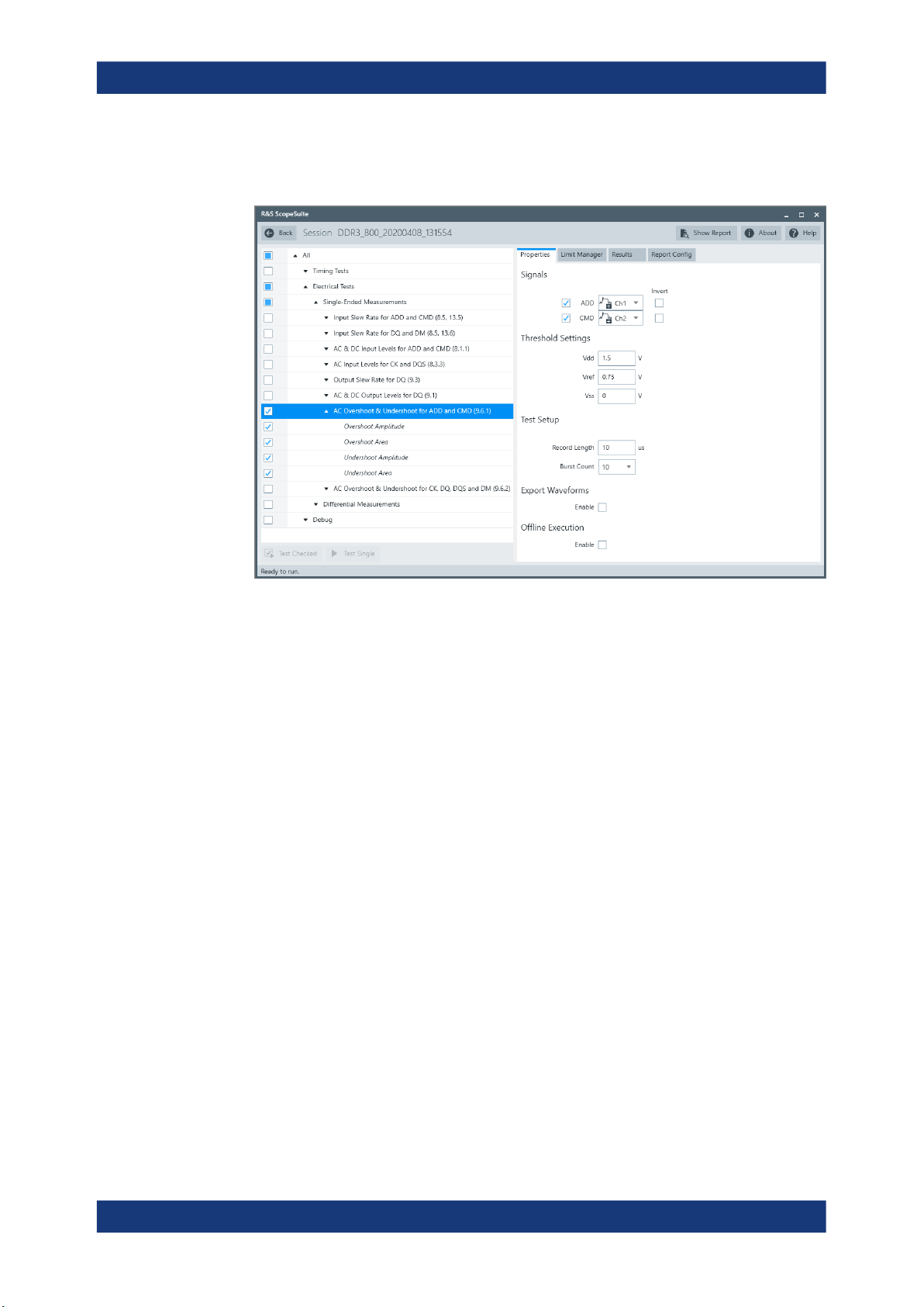
R&S®RTO-K91, R&S®RTO6-K91, R&S®RTP-K91
2. Select "Electrical Tests" > "Single-Ended Signals" > "AC Overshoot & Undershoot
for ADD and CMD".
Electrical Tests
Single-Ended Signals
3. Enable the "Signals" you want to use.
If only the ADD/CMD signal is selected, only ADD/CMD signal will be used to run
the test.
If both the ADD and the CMD signals are selected, test will be run using ADD signal first, followed by the CMD signal.
4. Enable the tests that you want to run.
5. Click "Test Single".
6. Follow the instructions of the step-by step guide.
When you have finished all steps, the compliance test runs automatically.
7. You can also run the test in offline mode, using downloaded waveforms. For
details, see Chapter 3.2.2, "Test Configuration for DDR3", on page 18.
5.1.7.3 Test Setup
The software guides you to make the proper connections. Follow the steps to conduct
the test.
The software is intended to facilitate the execution of a set of measurements on the relevant signals.
Consider also the soldering guide, see Chapter 2.1.1, "Soldering Guide for Modular
Probes", on page 9.
56User Manual 1178.8771.02 ─ 07
R&S®RTO-K91, R&S®RTO6-K91, R&S®RTP-K91
5.1.7.4 Measurements
The overshoot and undershoot for address and control measurements consist of up to
four measurements. It tests the limits as defined in section 9.6.1 (DDR3/DDR3L)/
8.5(LPDDR3) of the JESD79-3F(DDR3)/JESD79-3-1A-01(DDR3L)/
JESD209-3C(LPDDR3) specifications.
Overshoot Amplitude
This test aims to verify that the maximum peak amplitude allowed for overshoot area is
within the limits defined in the specification.
Overshoot Area
This test aims to verify that the maximum overshoot area above VDD is within the limits defined in the specification.
Undershoot Amplitude
This test aims to verify that the maximum peak amplitude allowed for undershoot area
is within the limits defined in the specification.
Electrical Tests
Single-Ended Signals
Undershoot Area
This test aims to verify that the maximum undershoot area below VSS is within the limits defined in the specification.
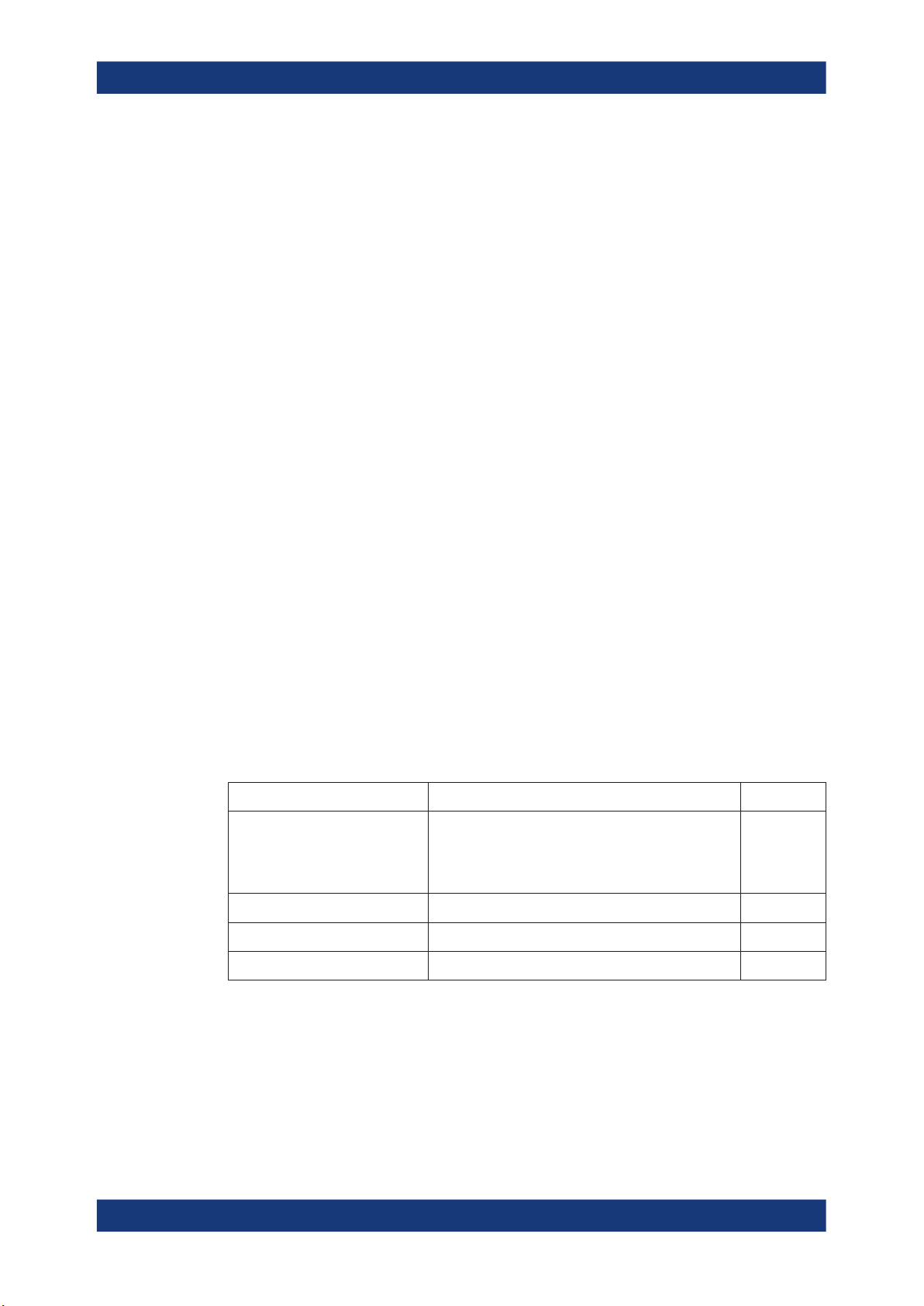
5.1.8 AC Overshoot & Undershoot for CK, DQ, DQS, and DM
5.1.8.1 Test Equipment
Item Description, model Quantity
Rohde & Schwarz oscilloscope R&S RTP with 4 channels and minimum 8 GHz band-
width
R&S RTO2000/RTO6 with 4 channels and minimum 4
GHz bandwidth
Modular Probe Probe with minimum 9 GHz bandwidth 4
Probe tip R&S RT-ZMA10 4
DUT DDR3 device that supports the selected type 1
1
5.1.8.2 Performing the Tests
1. Start the test as described in Chapter 3.5, "Starting DDR3 Tests", on page 23.
2. Select "Electrical Tests" > "Single-Ended Signals" > "AC Overshoot & Undershoot
for CK, DQ, DQS, and DM".
57User Manual 1178.8771.02 ─ 07
R&S®RTO-K91, R&S®RTO6-K91, R&S®RTP-K91
Electrical Tests
Single-Ended Signals
3. Enable the tests that you want to run.
4. Click "Test Single".
5. Follow the instructions of the step-by step guide.
When you have finished all steps, the compliance test runs automatically.
6. You can also run the test in offline mode, using downloaded waveforms. For
details, see Chapter 3.2.2, "Test Configuration for DDR3", on page 18.
5.1.8.3 Test Setup
The software guides you to make the proper connections. Follow the steps to conduct
the test.
The software is intended to facilitate the execution of a set of measurements on the relevant signals.
Consider also the soldering guide, see Chapter 2.1.1, "Soldering Guide for Modular
Probes", on page 9.
5.1.8.4 Measurements
The overshoot and undershoot for clock, data, strobe and mask measurements consist
of up to four measurements. It tests the limits as defined in section 9.6.2 (DDR3/
DDR3L)/ 8.5(LPDDR3) of the JESD79-3F(DDR3)/JESD79-3-1A-01(DDR3L)/
JESD209-3C(LPDDR3) specifications.
58User Manual 1178.8771.02 ─ 07

R&S®RTO-K91, R&S®RTO6-K91, R&S®RTP-K91
Overshoot Amplitude
This test aims to verify that the maximum peak amplitude allowed for overshoot area is
within the limits defined in the specification.
Overshoot Area
This test aims to verify that the maximum overshoot area above VDDQ is within the
limits defined in the specification.
Undershoot Amplitude
This test aims to verify that the maximum peak amplitude allowed for undershoot area
is within the limits defined in the specification.
Undershoot Area
This test aims to verify that the maximum undershoot area below VSSQ is within the
limits defined in the specification.
Electrical Tests
Differential Signals
5.2 Differential Signals
5.2.1 AC Input Levels for CK and DQS
5.2.1.1 Test Equipment
Item Description, model Quantity
Rohde & Schwarz oscilloscope R&S RTP with 4 channels and minimum 8 GHz band-
width
R&S RTO2000/RTO6 with 4 channels and minimum 4
GHz bandwidth
Modular Probe Probe with minimum 9 GHz bandwidth 2
Probe tip R&S RT-ZMA10 2
DUT DDR3 device that supports the selected type 1
5.2.1.2 Performing the Tests
1
1. Start the test as described in Chapter 3.5, "Starting DDR3 Tests", on page 23.
2. Select "Electrical Tests" > "Differential Signals" > "AC Input Levels for CK and
DQS".
59User Manual 1178.8771.02 ─ 07
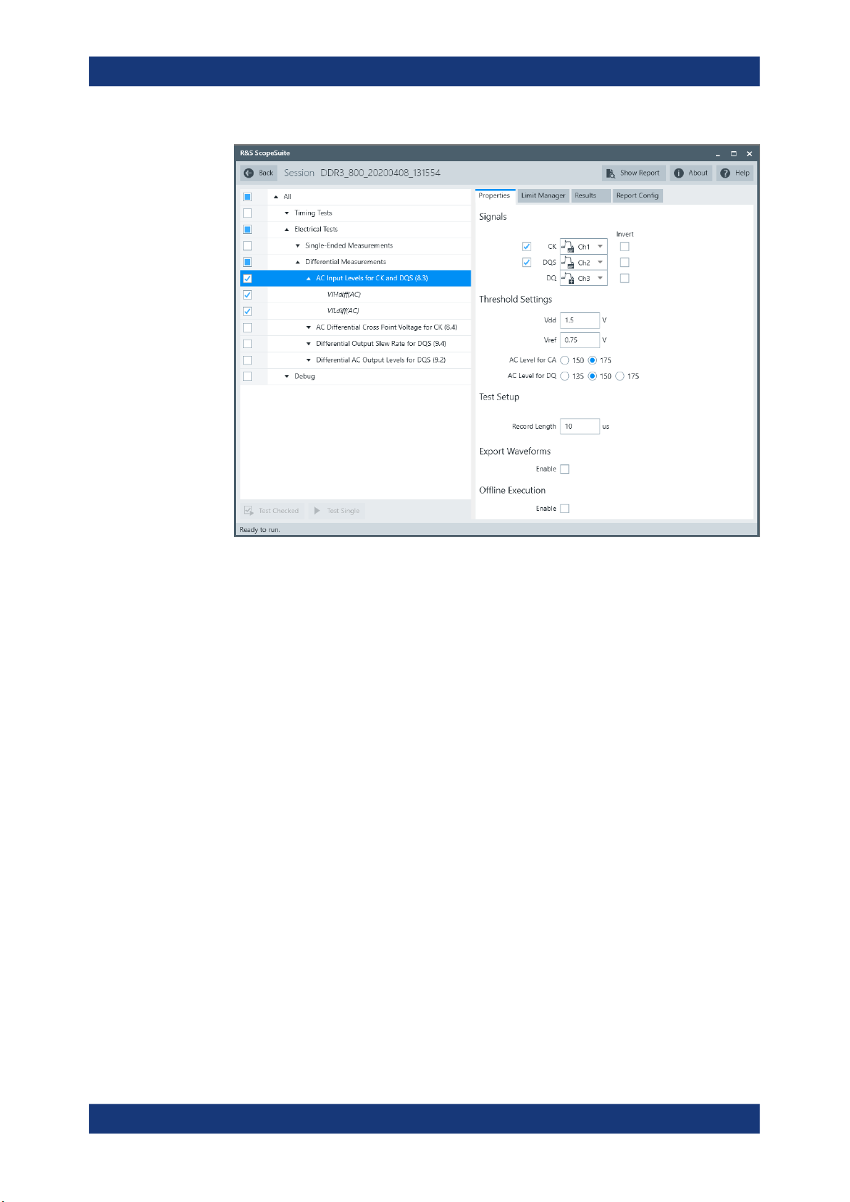
R&S®RTO-K91, R&S®RTO6-K91, R&S®RTP-K91
Electrical Tests
Differential Signals
3. Enable the tests that you want to run.
4. Click "Test Single".
5. Follow the instructions of the step-by step guide.
When you have finished all steps, the compliance test runs automatically.
6. You can also run the test in offline mode, using downloaded waveforms. For
details, see Chapter 3.2.2, "Test Configuration for DDR3", on page 18.
5.2.1.3 Test Setup
The software guides you to make the proper connections. Follow the steps to conduct
the test.
The software is intended to facilitate the execution of a set of measurements on the relevant signals.
Consider also the soldering guide, see Chapter 2.1.1, "Soldering Guide for Modular
Probes", on page 9.
5.2.1.4 Measurements
The differential AC input levels for clock and strobe measurements consist of up to two
measurements. It tests the limits as defined in section 8.3 (DDR3) / 10.1(DDR3L) /
7.4.2 (LPDDR3) of the JESD79-3F(DDR3)/JESD79-3-1A-01(DDR3L)/
JESD209-3C(LPDDR3) specifications.
60User Manual 1178.8771.02 ─ 07

R&S®RTO-K91, R&S®RTO6-K91, R&S®RTP-K91
Electrical Tests
Differential Signals
Differential Input High AC - V
IHdiff(AC)
This test aims to verify that the AC differential input high is within the limits defined in
the specification.
Differential Input Low AC - V
ILdiff(AC)
This test aims to verify that the AC differential input low is within the limits defined in
the specification.
5.2.2 AC Differential Cross Point Voltage for CK
5.2.2.1 Test Equipment
Item Description, model Quantity
Rohde & Schwarz oscilloscope R&S RTP with 4 channels and minimum 8 GHz band-
width
R&S RTO2000/RTO6 with 4 channels and minimum 4
GHz bandwidth
Modular Probe Probe with minimum 9 GHz bandwidth 3
1
Probe tip R&S RT-ZMA10 3
DUT DDR3 device that supports the selected type 1
5.2.2.2 Performing the Tests
1. Start the test as described in Chapter 3.5, "Starting DDR3 Tests", on page 23.
2. Select "Electrical Tests" > "Differential Signals" > "AC Differential Cross Point Voltage for CK".
61User Manual 1178.8771.02 ─ 07

R&S®RTO-K91, R&S®RTO6-K91, R&S®RTP-K91
Electrical Tests
Differential Signals
3. Enable the tests that you want to run.
4. Click "Test Single".
5. Follow the instructions of the step-by step guide.
When you have finished all steps, the compliance test runs automatically.
6. You can also run the test in offline mode, using downloaded waveforms. For
details, see Chapter 3.2.2, "Test Configuration for DDR3", on page 18.
5.2.2.3 Test Setup
The software guides you to make the proper connections. Follow the steps to conduct
the test.
The software is intended to facilitate the execution of a set of measurements on the relevant signals.
Consider also the soldering guide, see Chapter 2.1.1, "Soldering Guide for Modular
Probes", on page 9.
5.2.2.4 Measurements
The differential cross point voltage for clock measurement consists of one measurement. It tests the limits as defined in section 8.4 (DDR3) / 11(DDR3L) / 7.5 (LPDDR3)
of the JESD79-3F(DDR3)/JESD79-3-1A-01(DDR3L)/JESD209-3C(LPDDR3) specifications.
62User Manual 1178.8771.02 ─ 07
R&S®RTO-K91, R&S®RTO6-K91, R&S®RTP-K91
Electrical Tests
Differential Signals
Differential Input Cross Point Voltage - V
IX(AC)
This test aims to verify that the differential input cross point voltage is within the limits
defined in the specification. It is measured from the actual cross point of true and complement signals to the midlevel between of VDD and VSS.
5.2.3 Differential Output Slew Rate for DQS
5.2.3.1 Test Equipment
Item Description, model Quantity
Rohde & Schwarz oscilloscope R&S RTP with 4 channels and minimum 8 GHz band-
width
R&S RTO2000/RTO6 with 4 channels and minimum 4
GHz bandwidth
Modular Probe Probe with minimum 9 GHz bandwidth 2
Probe tip R&S RT-ZMA10 2
DUT DDR3 device that supports the selected type 1
1
5.2.3.2 Performing the Tests
1. Start the test as described in Chapter 3.5, "Starting DDR3 Tests", on page 23.
2. Select "Electrical Tests" > "Differential Signals" > "Differential Output Slew Rate for
DQS".
63User Manual 1178.8771.02 ─ 07

R&S®RTO-K91, R&S®RTO6-K91, R&S®RTP-K91
Electrical Tests
Differential Signals
3. Enable the tests that you want to run.
4. Click "Test Single".
5. Follow the instructions of the step-by step guide.
When you have finished all steps, the compliance test runs automatically.
6. You can also run the test in offline mode, using downloaded waveforms. For
details, see Chapter 3.2.2, "Test Configuration for DDR3", on page 18.
5.2.3.3 Test Setup
The software guides you to make the proper connections. Follow the steps to conduct
the test.
The software is intended to facilitate the execution of a set of measurements on the relevant signals.
Consider also the soldering guide, see Chapter 2.1.1, "Soldering Guide for Modular
Probes", on page 9.
5.2.3.4 Measurements
The differential output slew rate for strobe consists of up to two measurements. It tests
the limits as defined in section 9.4 (DDR3) / 9 (DDR3L) / 8.4 (LPDDR3) of the
JESD79-3F(DDR3)/JESD79-3-1A-01(DDR3L)/JESD209-3C(LPDDR3) specifications.
64User Manual 1178.8771.02 ─ 07

R&S®RTO-K91, R&S®RTO6-K91, R&S®RTP-K91
Slew Rate Query Output Differential Signals Rising- SRQdiff Rising
This test aims to verify that the differential output slew rate for rising edge is within the
limits defined in the specification. It is measured from VOLdiff(AC) to VOHdiff(AC).
Slew Rate Query Output Differential Signals Falling - SRQdiff Falling
This test aims to verify that the differential output slew rate for falling edge is within the
limits defined in the specification. It is measured from VOHdiff(AC) to VOLdiff(AC).
5.2.4 Differential AC Output Levels for DQS
5.2.4.1 Test Equipment
Item Description, model Quantity
Electrical Tests
Differential Signals
Rohde & Schwarz oscilloscope R&S RTP with 4 channels and minimum 8 GHz band-
Modular Probe Probe with minimum 9 GHz bandwidth 2
Probe tip R&S RT-ZMA10 2
DUT DDR3 device that supports the selected type 1
5.2.4.2 Performing the Tests
1. Start the test as described in Chapter 3.5, "Starting DDR3 Tests", on page 23.
2. Select "Electrical Tests" > "Differential Signals" > "Differential AC Output Levels for
DQS".
1
width
R&S RTO2000/RTO6 with 4 channels and minimum 4
GHz bandwidth
65User Manual 1178.8771.02 ─ 07

R&S®RTO-K91, R&S®RTO6-K91, R&S®RTP-K91
Electrical Tests
Differential Signals
3. Enable the tests that you want to run.
4. Click "Test Single".
5. Follow the instructions of the step-by step guide.
When you have finished all steps, the compliance test runs automatically.
6. You can also run the test in offline mode, using downloaded waveforms. For
details, see Chapter 3.2.2, "Test Configuration for DDR3", on page 18.
5.2.4.3 Test Setup
The software guides you to make the proper connections. Follow the steps to conduct
the test.
The software is intended to facilitate the execution of a set of measurements on the relevant signals.
Consider also the soldering guide, see Chapter 2.1.1, "Soldering Guide for Modular
Probes", on page 9.
5.2.4.4 Measurements
The differential AC output levels for strobe measurements consist of up to two measurements. It tests the limits as defined in section 9.2 (DDR3/DDR3L) / 8.2(LPDDR3)
of the JESD79-3F(DDR3)/JESD79-3-1A-01(DDR3L)/JESD209-3C(LPDDR3) specifications.
66User Manual 1178.8771.02 ─ 07

R&S®RTO-K91, R&S®RTO6-K91, R&S®RTP-K91
V
OHdiff(AC)
This test aims to verify that the AC differential output high measurement level for the
output slew rate is within the limits defined in the specification.
V
OLdiff(AC)
This test aims to verify that the AC differential output low measurement level for the
output slew rate is within the limits defined in the specification.
Electrical Tests
Differential Signals
67User Manual 1178.8771.02 ─ 07

R&S®RTO-K91, R&S®RTO6-K91, R&S®RTP-K91
6 Debug Tests
6.1 Trigger Write Cycle
6.1.1 Test Equipment
Item Description, model Quantity
Debug Tests
Trigger Write Cycle
Rohde & Schwarz oscilloscope R&S RTP with 4 channels and minimum 8 GHz band-
Modular Probe Probe with minimum 9 GHz bandwidth 3
Probe tip R&S RT-ZMA10 3
DUT DDR3 device that supports the selected type 1
6.1.2 Performing the Tests
1. Start the test as described in Chapter 3.5, "Starting DDR3 Tests", on page 23.
2. Select "Debug" > "Trigger Write Cycle".
1
width
R&S RTO2000/RTO6 with 4 channels and minimum 4
GHz bandwidth
68User Manual 1178.8771.02 ─ 07
R&S®RTO-K91, R&S®RTO6-K91, R&S®RTP-K91
3. Enable the tests that you want to run.
4. Click "Test Single".
5. Follow the instructions of the step-by step guide.
When you have finished all steps, the compliance test runs automatically.
6. You can also run the test in offline mode, using downloaded waveforms. For
details, see Chapter 3.2.2, "Test Configuration for DDR3", on page 18.
6.1.3 Test Setup
The software guides you to make the proper connections. Follow the steps to conduct
the test.
The software is intended to facilitate the execution of a set of measurements on the relevant signals.
Consider also the soldering guide, see Chapter 2.1.1, "Soldering Guide for Modular
Probes", on page 9.
Debug Tests
Trigger Read Cycle
6.1.4 Measurements
This test case helps you to see the signals of CK, DQS, DQ during the write operation
of DDR3. The signals are triggered to make the write bursts visible
6.2 Trigger Read Cycle
6.2.1 Test Equipment
Item Description, model Quantity
Rohde & Schwarz oscilloscope R&S RTP with 4 channels and minimum 8 GHz band-
Modular Probe Probe with minimum 9 GHz bandwidth 3
Probe tip R&S RT-ZMA10 3
DUT DDR3 device that supports the selected type 1
1
width
R&S RTO2000/RTO6 with 4 channels and minimum 4
GHz bandwidth
6.2.2 Performing the Tests
1. Start the test as described in Chapter 3.5, "Starting DDR3 Tests", on page 23.
69User Manual 1178.8771.02 ─ 07

R&S®RTO-K91, R&S®RTO6-K91, R&S®RTP-K91
2. Select "Debug" > "Trigger Read Cycle".
Debug Tests
Trigger Read Cycle
3. Enable the tests that you want to run.
4. Click "Test Single".
5. Follow the instructions of the step-by step guide.
When you have finished all steps, the compliance test runs automatically.
6. You can also run the test in offline mode, using downloaded waveforms. For
details, see Chapter 3.2.2, "Test Configuration for DDR3", on page 18.
6.2.3 Test Setup
The software guides you to make the proper connections. Follow the steps to conduct
the test.
The software is intended to facilitate the execution of a set of measurements on the relevant signals.
Consider also the soldering guide, see Chapter 2.1.1, "Soldering Guide for Modular
Probes", on page 9.
6.2.4 Measurements
This test case helps you to see the signals of CK, DQS, DQ during the read operation
of DDR3. The signals are triggered to make the read bursts visible.
70User Manual 1178.8771.02 ─ 07
 Loading...