


Roadstar
DVD-2010H
SERVICE MANUAL

1. GENERAL DESCRIPTION
Major functional blocks are discussed briefly in this section. A more detailed description is contained later in the
document.
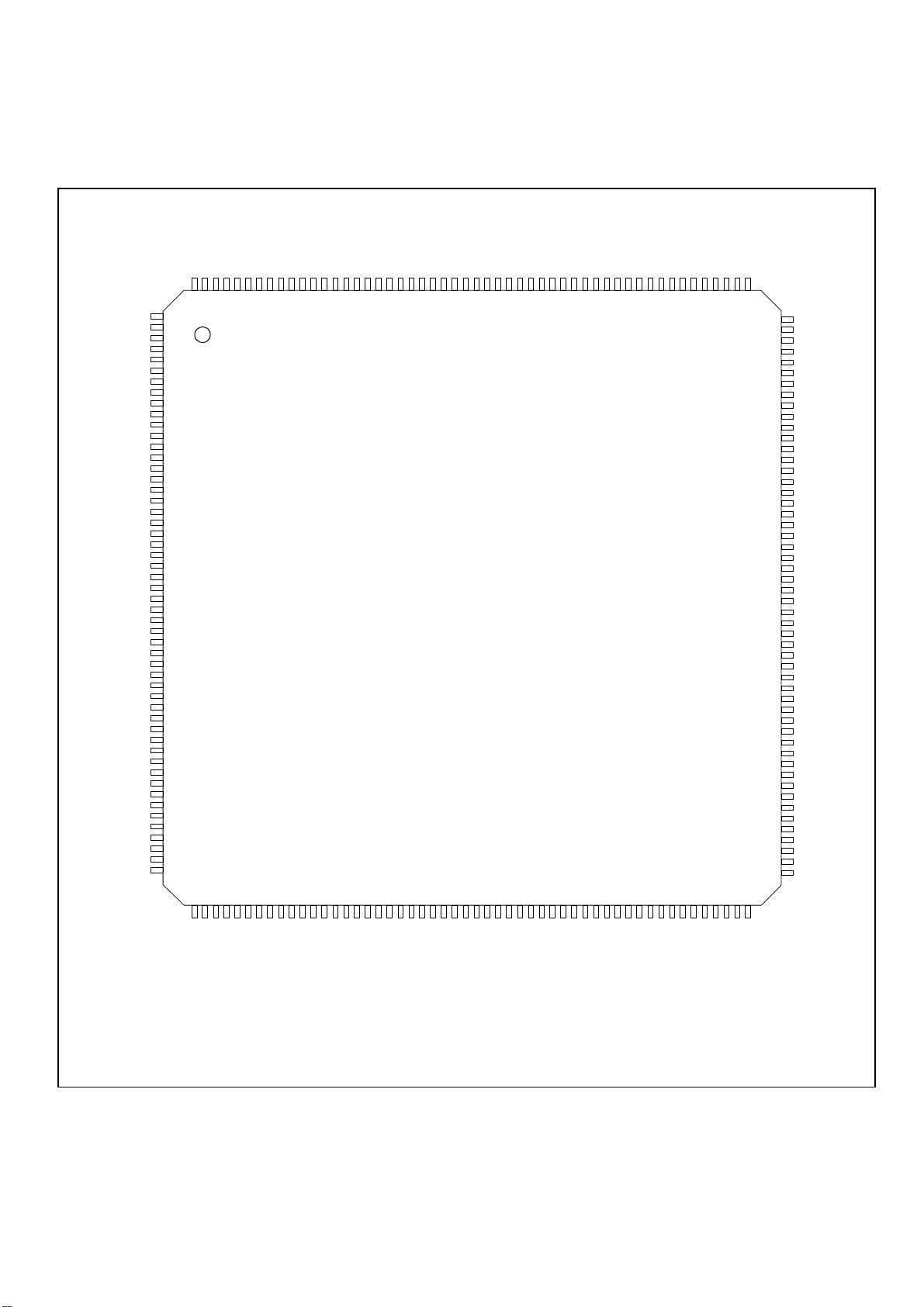
1.1 STi5519
The STi5519 provides a highly integrated back-end solution for DVD applications. A host CPU handles
both the general application (the user interface, and the DVD, CD-DA, VCD, SVCD navigation) and the
drivers of the different embedded peripheral (audio/video, sub-picture decoders, OSD,
PAL/NTSC encoder...)
These functions include:
Integrated 32-bit host CPU @ 60MHz
- 2 Kbytes of instruction cache, 2 Kbytes of data cache, and 4Kbytes of SRAM configurable as
data cache.
Audio decoder
- 5.1 channel Dolby Digital® /MPEG-2 multi-channel decoding, 3 X 2-channel PCM outputs
- IEC60958 - IEC61937 digital output
- DTS® digital out 5.1 channel
- SRS®/TruSurround®
- MP3 decoding
Video decoder
- Supports MPEG-2 MP@ML
- Fully programmable zoom-in and zoom-out
- PAL to NTSC and NTSC to PAL conversion
DVD and SVCD subpicture decoder
High performance on-screen display
- to 8 bits per pixel OSD options
- Anti-flicker, anti-flutter and anti-aliasing filters
PAL/NTSC/SECAM encoder
- RGB, CVBS, Y/C and YUV outputs with 10-bit DACs
- Macrovision® 7.01/6.1 compatible
Shared SDRAM memory interface
- Supports one or two 16Mbit, or one 64Mbit 125 MHZ SDRAMs
Programmable CPU memory interface for SDRAM, ROM, peripherals...
Front-end interface
- DVD, VCD, SVCD and CD-DA compatible
- Serial, parallel and ATAPI interfaces
- Hardware sector filtering
- Integrated CSS decryption and track buffer
Integrated peripherals
- UARTS, 2 SmartCards, I2C controller, 3 PWM outputs, 3 capture timers
- Modem support
- 38 bits of programmable I/O
Please refer to the STi5519 Data Sheets: STi5519 DVD HOST PROCESSOR WITH ENHANCED
AUDIO FEATURES and STi5519 REGISTER MANUAL for more detailed information.
1.2 MEMORY
The STi5519 includes all of the interface signals to connect to industry standard SDRAM, DRAM, ROM, and I2C
memory devices. The system includes one or two SDRAM components. The MPEG decoder unit interfaces to a single
4M x 16bit SDRAM over the SMI bus. The general purpose processor can share the decoder SDRAM or can access
an optional SDRAM installed on the EMI bus. This EMI SDRAM can be either a 1Mx16 or 4Mx16 chip. The optional
EMI SDRAM can be installed if the system requires higher performance of requires more RAM than is standard
system (due to complex trick modes, advanced GUI, etc). The standard production executes without EMI SDRAM

installed, A single 1Mx16 FLASH ROM device is support on the EMI bus. There is also a 2kb I2C serial EEPROM
for storage of user player settings, software configuration information, title specific information, or other purposes.
1.3 DRIVE INTERFACES
The system supports a standard ATAPI drive interface.
The interface to the ATAPI drive is included within the STi5519. The ATAPI data bus is buffered so that the ATAPI
cable does not interfere with signal quality. An ATAPI drive is connected via the standard 34 pin dual row PC style IDE
header
1.4 FRONT PANEL
The front panel is based around an Futaba VFD and a common NEC front panel controller chip, (uPD16311). The
STi5519 controls the uPD16311 using several control signals, (clock, data, chip select). The infra-red remote control
signal is passed directly to the STi5519 for decoding.
1.5 OUTPUTS
There is no separate rear panel for outputs. They are embedded into the mainboard. Supported outputs are:
- Six channel or two channel audio outputs
- Optical and coax S/PDIF outputs are supported
- Composite, S-Video, and SCART outputs
The six video signals used to provide CVBS, S-Video, and RGB are generated by the STi5519's internal video DAC.
The video signals are be buffered by external circuitry.
Six channel audio output by the STi5519 in the form of three I2S (or similar) data streams. The S/PDIF serial stream is
also generated by the STi5519. Three pieces two-channel audio DACs (CS4335) are used for six channel audio
output, and similarly only one CS4335 DAC is used for two channel audio output.
2 GPIO, IRQ, AND CHIP SELECT ASSIGNMENTS
PIO Port Bit Pin # STi5519 Alternate Function Software Function
P in data
P IO2[5]
P IO2[6]
P IO2[7]
V DD3_ 3
V S S
P IO3[0]
P IO3[1]
P IO3[2]
P IO3[3]
P IO3[4]
P IO3[5]
P IO3[6]
P IO3[7]
V DD2_ 5
V S S
B _DATA
B _B C LK
B _F LA G
B _S Y NC
P IO5[0]
P IO5[1]
P IO5[2]
VD D_R G B
V S S_ R G B
B _O UT
G _OUT
R _O UT
V_ R E F _R G
I_R E F _R G
V DD_Y C C
V S S _YC C
Y _O UT
C _OU T
C V_ OUT
V _R E F _Y C
I_ RE F_ YC
V DD2_ 5
V S S
P IO4[0]
P IO4[1]
P IO4[2]
P IO4[3]
P IO4[4]
P IO4[5]
P IO4[6]
P IO4[7]
V DD3_ 3
VD D_P C M
V S S_ P CM
V S S
DAC _S CL K
DA C_ P C MOU T0
P IO2[4]
P IO2[3]
P IO2[2]
P IO2[1]
P IO2[0]
T R IGG E R _O UT
T RIG GE R _I N
P IO1[5]
P IO1[4]
V S S
VD D2_ 5
P IO1[3]
P IO1[2]
P IO1[1]
P IO1[0]
P IO0[7]
P IO0[6]
P IO0[5]
P IO0[4]
P IO0[3]
P IO0[2]
P IO0[1]
P IO0[0]
V S S
VD D3_ 3
C PU _ADR [21]
C PU _ADR [20]
C PU _ADR [19]
C PU _ADR [18]
C PU _ADR [17]
C PU _ADR [16]
C PU _ADR [15]
C PU _ADR [14]
C PU _ADR [13]
C PU _ADR [12]
C PU _ADR [11]
V S S
VD D2_ 5
C PU _ADR [10]
C PU _ADR [9]
C PU _ADR [8]
208
207
206
205
204
203
202
201
200
199
198
197
196
195
194
193
192
191
190
189
188
187
186
185
184
183
182
181
180
179
178
177
176
175
174
173
172
171
170
169
1
2
3
4
5
6
7
8
9
10
11
12
13
14
15
16
17
18
19
20
21
22
23
24
25
26
27
28
29
30
31
32
33
34
35
36
37
38
39
40
41
42
43
44
45
46
47
48
49
50
51
52
5354555657585960616263646566676869707172737475767778798081828384858687888990919293949596979899
S Ti5519
P QF P 208
(rev F )
168
C PU _ADR [7]
C PU _ADR [6]
C PU _ADR [5]
C PU _ADR [4]
C PU _ADR [3]
C PU _ADR [2]
C PU _ADR [1]
V S S
VD D3_ 3
C PU _DATA [15]
C PU _DATA [14]
167
166
165
164
163
162
161
160
159
158
157
15 6
C PU _DATA [13]
15 5
C PU _DATA [12]
15 4
C PU _DATA [11 ]
C PU _DATA [10]
15 3
C PU _DATA [9]
15 2
15 1
C PU _DATA [8]
15 0
V S S
14 9
V DD2_ 5
14 8
C PU _DATA [7]
C PU _DATA [6]
14 7
C PU _DATA [5]
14 6
14 5
C PU _DATA [4]
14 4
C PU _DATA [3]
14 3
C PU _DATA [2]
14 2
C PU _DATA [1]
C PU _DATA [0]
14 1
C PU _C AS 1
14 0
13 9
C PU _C AS 0
13 8
C PU _R AS 1
13 7
V S S
13 6
V DD3_ 3
C PU _C E[0 ]
13 5
C PU _C E[1 ]
13 4
13 3
C PU _C E[2 ]
13 2
C PU _C E[3 ]
13 1
C PU _WA IT
13 0
C PU _R W
C PU _B E [1]
12 9
C PU _B E [0]
12 8
12 7
IR Q [0]
12 6
IR Q [1]
12 5
IR Q [2]
12 4
R E S E T
V S S_ P LL
12 3
V DD_P L L
12 2
12 1
V S S
12 0
P IX_C L K
11 9
V DD2_ 5
11 8
C PU _P R OC LK
C PU _OE
11 7
P WM0
11 6
11 5
P WM1
11 4
P WM2
11 3
T C K
11 2
T DI
T DO
111
T MS
11 0
10 9
T R S T
10 8
V S S
10 7
V DD3_ 3
10 6
res erved
P IO5 [5]
10 5
100
101
102
103
104
V S S
VD D2_ 5
S MI_ADR [4]
S MI_ADR [5]
S MI_ADR [6]
S MI_ADR [7]
S MI_ADR [8]
S MI_ADR [9]
S MI_ADR [3]
S MI_ADR [2]
S MI_ADR [1]
S P DIF _O UT
DA C_ LR C LK
DAC _P C MCL K
DAC _P C MOU T1
DAC _P C MOU T2
S MI_ADR [0]
S MI_ADR [11]
S MI_ ADR [1 0]
S MI_ ADR [1 2]
S MI_ ADR [1 3]
S MI_WE
S MI_R AS
S MI_CAS
S MI_ C S [0]
S MI_ C S [1]
V S S
VD D3_ 3
S MI_ DQ ML
S MI_CLK IN
S MI_ DQ MU
S MI_ DATA [0]
S MI_ DATA [1]
S MI_ DATA [2]
S MI_ DATA [3]
S MI_ DATA [4]
S MI_ DATA [5]
S MI_ DATA [6]
S MI_ DATA [7]
V S S
VD D2_ 5
S MI_ DATA [8]
S MI_ DATA [9]
S MI_ C LK OU T
S MI_ DATA [11]
S MI_ DATA [10]
P IO5 [3]
P IO5 [4]
S MI_ DATA [12]
S MI_ DATA [13]
S MI_ DATA [14]
S MI_ DATA [15]

PIO Port Bit Pin # STi5519 Alternate Function CineMaster CE Function
Port 0 Bit 0
Port 0 Bit 1
Port 0 Bit 2
Port 0 Bit 3
Port 0 Bit 4
Port 0 Bit 5
Port 0 Bit 6
Port 0 Bit 7
Port 1 Bit 0
Port 1 Bit 1
Port 1 Bit 2
Port 1 Bit 3
Port 1 Bit 4
Port 1 Bit 5
Port 1 Bit 6
Port 1 Bit 7
Port 2 Bit 0
Port 2 Bit 1
Port 2 Bit 2
Port 2 Bit 3
Port 2 Bit 4
Port 2 Bit 5
Port 2 Bit 6
Port 2 Bit 7
Port 3 Bit 0
Port 3 Bit 1
Port 3 Bit 2
Port 3 Bit 3
Port 3 Bit 4
Port 3 Bit 5
Port 3 Bit 6
Port 3 Bit 7
Port 4 Bit 0
Port 4 Bit 1
Port 4 Bit 2
Port 4 Bit 3
Port 4 Bit 4
Port 4 Bit 5
Port 4 Bit 6
Port 4 Bit 7
186
187
188
189
190
191
192
193
194
195
196
197
200
201
202
203
204
205
206
207
208
1
2
3
6
7
8
9
10
11
12
13
39
40
41
42
43
44
45
46
SC0_DATA
#ATAPI_RD
#ATAPI_WR
SC0_CLK
SC0_RST
SC0_CMD_VCC
SC0_DATA_DIR
SC0_DETECT
SSC0_DATA
SSC0_CLK
PARA_DVALID/SC_EXT_CLK
TXD2
RXD2
PARA_SYNC/TXD1
TRIGIN
TRIGOUT
SC1_DATA
PARA_REQ/RXD1
PARA_STR
SC1_CLK
SC1_RST
SC1_CMD_VCC
DAC_DATA/SC1_DATA_DIR
SC1_DETECT
PARA_DATA0
PARA_DATA1
PARA_DATA2
PARA_DATA3
PARA_DATA4
PARA_DATA5
PARA_DATA6/COMP1
PARA_DATA7/COMP2
YUV0
YUV1
YUV2
YUV3
YUV4
YUV5
YUV6
YUV7
#SOFT_RESET
#ATAPI_RD
#ATAPI_WR
DAC_CCLK (Audio DAC control)
DAC_CDTI (Audio DAC control)
#DAC_CS0 (Audio DAC control)
#DAC_CS1 (Audio DAC control)
Unused (Test Point 39)
SDA (I2C)
SCL (I2C)
Unused (Test Point 35)
TXD (Serial Port)
RXD (Serial Port)
SR0 (for PLL1700)
TRIGIN (JTAG)
TRIGOUT (JTAG)
FPCLK (Front Panel)
FS0 (for PLL1700)
FS1 (for PLL1700)
RTS (Serial Port)
CTS (Serial Port)
FPDATA (Front Panel)
DAC_DATA (Stereo Audio)
FPSTRB (Front Panel)
OPEN (TMM Tray Control)
CLOSE (TMM Tray Control)
Unused (Test Point 36)
Front Panel IR
Unused (Test Point 37)
Unused (Test Point 38)
#SENSE (TMM Tray Control)
#PUSH (TMM Tray Control)
YUV0 (External Video DENC)
YUV1
YUV2
YUV3
YUV4
YUV5
YUV6
YUV7
* Front Panel uses the 16311 controller. In the CineMaster design, FPDIN and FPDOUT are connected
together as FPDATA.

3. AUDIO OUTPUT
The STi5519 supports a six channel analog output. In a system configuration with six analog outputs, the front left and
right channels can be configured to provide the stereo (2 channel) outputs and Dolby Surround, or the left and right front
channels for a 5.1 channel surround system.
The Sti5519 also provides digital output in S/PDIF format. The board supports both optical and coaxial S/PDIF outputs.
3.1 AUDIO DACS
The STi5519 supports several variations of an I2S type bus, varying the order of the data bits (leading or no leading zero
bit, left or right alignment within frame, and MSB or LSB first) is possible using the Sti5519 internal configuration registers. The I2S format uses four stereo data lines and three clock lines. The I2S data and clock lines can be connected
directly to one or more audio DAC to generate analog audio output.
The two-channel DAC is an Cirrus Logic CS4335. The DACs support up to 96kHz sampling rate.
The outputs of the DACs are differential, not single ended so a buffering circuit is required. The buffer circuits use National
LM833 op-amps to perform the low-pass filtering and the buffering.
4 VIDEO INTERFACE
The STi5519 integrates a PAL/NTSC encoder. It converts the digital MPEG/Sub Picture/OSD
stream into a standard analog baseband PAL/NTSC signals. Six analog video outputs provide CVBS, Svideo (Y/C), and
RGB formats. The three RGB signals can be configured via an internal STi5519 register setting.
The encoder handles interlaced and non-interlaced mode. It can perform Closed Captions, CGMS or Teletext encoding
and allows Macrovision 7.01/6.1 copy protection. The encoder supports both master and slave modes for synchronization.
The buffered CVBS video is available on a RCA (cinch) style jack, S-Video on a mini-DIN and all six signals (and stereo
audio) are available on a SCART connector.
5 MPEG DECODER SDRAM MEMORY
The STi5519 includes glueless interfaces to SDRAM memory for the MPEG decoder. The STi5519 supports one or two
1Mx16bit chips or a 4Mx16bit SDRAM chip. However, the board
supports only a 64Mbit chip. The device used is a 4M x 16 bit, 125MHz, 3.3V, 54 pin TSOP II, Micron Technology
MCT48LC4M16A2TG-7 or equivalent.
6 FLASH MEMORY
The decoder board supports a single 1Mx16bit FLASH memory device. The device is a 1M x 16, 90ns, bottom boot
block, 3.3V, 48 pin TSOP II, 29F800 or equivalent.
7 SERIAL EEPROM MEMORY
An I2C serial EEPROM is used to store user configuration (i.e. language preferences, speaker setup, etc.) and software
configuration information (i.e. remote control type). Industry standard EEPROM range in size from 1kbit to 256kbit and
share the same IC footprint and pinout. The default device is 2kbit, 256kx 8, SOIC8 SGS Thomson ST24C02M1 or
equivalent.
8 ATAPI DRIVE INTERFACE
The STi5519 includes a glueless ATAPI interface on-chip. While this interface limits performance of the system, it is a
lower cost solution than providing external logic to interface the drive to the STi5519 frontend interface.
Note: The decoder board supports the standard ATAPI electrical connections, but the software protocol within the drive is
not always supported according to ATAPI specifications. Custom software may need to be developed and tested to
support ATAPI drives from different manufacturers.

9 AUDIO SAMPLING RATE AND EXTERNAL PLL COMPONENT CONFIGURATION
The decoder board has optional PLLs, which can be installed to provide the audio clock for the system. The initial version
of the STi5505 was not able to provide an audio clock for 96kHz support and an external PLL was used to support this.
This was fixed in the STi5505 later chip revisions and therefore no problems are expected in the STi5519. However, in
case a problem arises, the PLL circuit can be installed to provide a high quality clock particularly important in S/PDIF
applications.
In the default configuration, a small buffer chip is installed to buffer the audio clock between the STi5519 and the audio
DACs.
10 FRONT PANEL
10.1 VFD CONTROLLER
The VFD controller is a NEC uPD16311. This controller is not a processor, but does include a simple state machine
which scans the VFD and reads the front panel button matrix. The 16311 also includes RAM so it can store the current
state of all the VFD icons and segments. Therefore, the 16311 need only be accessed when the VFD status changes and
when the button status is read. The STI5519 can control this chip directly using PIO pins or can allow the front panel PIC
to control the VFD.
11 MISCELLANEOUS FUNCTIONS
11.1 RESET CIRCUITRY
Two different chips are supported to provide the power-on-reset and pushbutton reset function:
Telcom Semiconductor TC1270, or Dallas DS1811.
11.2 VOLTAGE REGULATORS
There are two +5V linear regulators to generate +5V for the analog circuitry from +12V. A smaller DPAK surface mount
device can be used in most circumstances, but in applications were more than 150mA are required, a TO-220 throughhole package can be used.
The STi5519 requires 2.5V to operate. This voltage is generated from +5V.
12 CONNECTORS
12.1 ATAPI DRIVE STANDARD CONNECTOR
12.2 STI5519 JTAG INTERFACE
12.3 SCART CONNECTORS
12.4 POWER CONNECTOR
13. VESTEL DVD DECODER CIRCUIT DESCRIPTION
13.1 POWER SUPPLY:
· Socket PL1 is the 220VAC input.
· Socket PL4 is used for the power button on the front panel.
· 2.5A fuse F1 is used to protect the device against short circuit.
· Line filters and capacitors TR2, C2, TR4 and C3 are used to block the parasitic coming from the
mains. They also prevent the noise, produced in the circuit, from being injected to the line.
· Voltage is rectified by using diodes D1, D5, D6 and D4. Using capacitor C1 (100mf) a DC voltage
is produced. (310- 320VDC).

· The current in the primary side of the transformer TR3 comes to the SMPS IC (IC3 TOP223Y). The
SMPS IC has a three-pin TO-220 case and a cooler is mounted on it. It has a built-in oscillator,
overcurrent and overvoltage protection circuitry and runs at 100kHz. It starts with the current from
the primary side of the transformer and follows the current from the feedback winding.
· Feedback current is rectified with diode D7 and filtered with capacitor C4 and enters the
optocoupler IC2 (CQY80NG). Depending on the control current coming from the secondary side,
SMPS IC keeps the output voltage constant by controlling the duty cycle of the 100kHz signal
(PWM) at the primary side of the transformer.
· Voltages on the secondary side are as follows: -12 Volts at D8, 5 Volts at D9, 15 Volts at D10, 22 Volts at D13.
· Using resistors R5, R4 and R27, 5V output is divided properly for D14 operation.
· D14 TL431 is a constant current regulator. TL431 watches the 5 volts and supplies the required
current to IC2. There are a LED and a photo transistor in IC2. The LED inside the IC2 transmits the
value of the current from D14 to phototransistor. Depending on the current gain of the
phototransistor IC3 keeps the voltage on the 5-volt-winding constant.
· Adjustable voltage regulator IC5 (LM317) supplies 12 Volts. 12 Volts is obtained by using resistors R19, R20 and R21.
· When the device enters stand-by mode, transistor Q2 starts to conduct and pulls the adjust pin of
IC5 to ground, where this cuts 12Volts off.
· IC6 is also an LM317 that produces 3.3 Volts output from its 5 volts input.
· 22 Volts is used to feed the VFD (Vacuum Fluorescent Display) driver IC on the front panel.
Using diode D17 22V is decreased about 5.6V and connected to the filament winding to produce the DC offset for the filaments.
· Transistor Q3 and zener diode D18 are used to regulate +12 Volts. This voltage is used to feed
op-amps on the back panel.
TOP
TOPS
T
hree-terminal Off-lin
Lowest cost, lowest component count switcher solution
Cost competitive with linears above 5W
Very low AC/DC losses Ð up to 90% efficiency
Built-in Auto-restart and Current limiting
Latching Thermal shutdown for system level protection
Implements Flyback, Forward, Boost or Buck topology
Works with primary or opto feedback
Stable in discontinuous or continuous conduction mode
Source connected tab for low EMI
Circuit simplicity and Design Tools reduce time to market
D
escription
The second generation TOPSwitch-II family is more cost
effective and provides several enhancements over the first
generation TOPSwitch family. The TOPSwitch-II family extends
the power range from 100W to 150W for 100/115/230 VAC
input and from 50W to 90W for 85-265 VAC universal input.
This brings TOPSwitch technology advantages to many new
applications, i.e. TV, Monitor, Audio amplifiers, etc. Many
significant circuit enhancements that reduce the sensitivity to
board layout and line transients now make the design even
221-227
¨
witch
P
r
oduct
-
II
H
ighlights
F
e
PW
a
mily
M
S
witc
h
AC
I
N
D
CONTR
OL
TOPS
Figure 1. Typical Flyback Application.
easier. The standard 8L PDIP package option reduces cost in
lower power, high efficiency applications. The internal lead
frame of this package uses six of its pins to transfer heat from
the chip directly to the board, eliminating the cost of a heat sink.
TOPSwitch incorporates all functions necessary for a switched
mode control system into a three terminal monolithic IC: power
MOSFET, PWM controller, high voltage start up circuit, loop
compensation and fault protection circuitry.
witch
S
C
PI-1951-091996

13.2 FRONT PANEL:
· All the functions on the front panel are controlled by U1 (Sti5519) on the mainboard.
· U1 sends the commands to IC2 uPD16311 via socket PL1 (pins 3,4 and 5).
· There are 16 keys scanning function, 2 LED outputs, 1 Stand-by output and VFD drivers on IC2.
· Pin 52 is the oscillator pin and is connected via R5 56K.
· LED D6 is red in stand-by mode and green when the device is on. When entering stand-by mode,
pin 48 goes HIGH (+5V) and controls the transistor Q2 on the power board.
· Vacuum fluorescent display MD2 is specially designed for DVD.
· The scanned keys are transmitted via IC2 pin 5 and 6 to U1 on the mainboard.
· IR remote control receiver module IC3 (TSOP1836) sends the commands from the remote control
directly to U1.
· Socket PL2 carries the VFD filament voltage and 22 Volts.
13.3 Outputs:
· There are 1 SCART connector (PL5), 6 pieces RCA audio jacks JK1, for audio output, 1 coaxial
digital audio output JK3 and 1 laser digital audio output MD1 on the back panel.
· TOTX178 is used for laser output.
· SPDIF enters the pins 1,3,5,9, and 11 of IC25. Connecting gates in parallel a buffer is constructed.
C166 is used for DC coupling. Resistors R181 and R182 divide the signal, which is transmitted
out via JK3 (RCA jack)
· Audio outputs are on JK1.
· Q145 through Q148 are used to suppress the noises during turn on and turn off.
· There are two op-amps in each IC18, IC19 and IC20 and they are used for six audio channels.
IC18 is used for front channels, Resistors R137,R190 and R158 are used to adjust the gain and
using R156 and C116 a filter circuit is created for the left channel. For front right channel, these
components are R140, R191 and R149 for gain, R151 and C113 for filter. For the remaining four
channels IC19 and IC20 are used with the corresponding resistors and capacitors connected in
similar way.
· Op-amp outputs the front left audio via C124 and R162 to RCA jack and via C123 and R161 to
SCART. Front right audio is sent to RCA its jack via C127, R164 and sent to SCART via C126
and R163.
· SCART pin 8 is controlled using transistors Q21 and Q22 to switch between modes 4:3 and 16:9 .
· When the BPPIO0 becomes 5 Volts, 4:3 mode is selected and 16:9 mode is selected when this
output becomes 0. The circuit is adjusted to output 12 Volts for 4:3 mode and 6 Volts for 16:9
mode.
· Transistors Q26 and Q24 transmits these voltages when the device is turned on and cuts them off
when the unit is turned off.
· LUMA and CHROMA signals of S-Video are transmitted to JK4 (S-Video socket) via transistors
Q12 and Q13 respectively.

COMPONENT
20071874 MAINBOARD CHS. DVD-3000 (MAN) DVS-2CH PC 1.000 . . . . .
POSITION NUMBER
2CHMP3-3000
SPARE PART LIST
NOTE: YOU CAN FIND SPARE PART CODES FOR MODEL- DEPENDENT PARTS IN OUR SERVICE WEB SITE : www.vestelservice.com
20071876 POWER BOARD CHS.DVD-3000 (MAN)(5508-DVS) PC 1.000 . . . . .
20092998 SCART ASSY DVD-3000 (MAN) (FERRITE') PC 1.000 . . . . .
20100796 FRONT PANEL DVD3000 (MAN) (SC FERRITE') PC 1.000 . . . . .
30000158 CAP MKP 4.7NF 630V J PC 1.000 C28 . . . .
30000423 CAP EL 47UF 400V M PC 1.000 C1 . . . .
30001155 RES MO 2W 33K J PC 1.000 R18 . . . .
30001284 DIODE 1N4148 0.15A/100V 0.5A PC 1.000 D7 . . . .
30001302 DIODE BYW29-200 8A/200V 80A PC 1.000 D9 . . . .
30001318 DIODE BA159 1A/800V 20A PC 3.000 D8 D13 D16 . .
30001329 DIODE 1N4007 1A/1000V 30A PC 4.000 D1 D4 D5 D6 .
30001343 DIODE ZENER 5.6V PC 1.000 D17 . . . .
30001350 DIODE ZENER 12V PC 1.000 D18 . . . .
30001453 TR BC337 PC 1.000 Q3 . . . .
30001454 TR BC548B PC 1.000 Q2 . . . .
30001503 IC CQY80NG (OPT.COUPLER) PC 1.000 IC2 . . . .
30001506 IC TL431 PC 1.000 D14 . . . .
30001731 FUSE 2.5A 250V 5*20MM PC 1.000 F1 . . . .
30010501 R/C DVD (BLACK) PC 1.000 . . . . .
30010700 DIODE BYV28-200 3.5A/200V 90A PC 1.000 . . . . .
30010798 IC TOP223Y PC 1.000 IC3 . . . .
30011787 POWER CORD ASSY.(2.4MT W/FTZ)-SATELLITE- PC 1.000 . . . . .
30012923 DVD LOADER (ATAPI INTERFACE) PC 1.000 . . . . .
30012968 CONN ASSY 4/20 POWER (5.00 mm) PC 1.000 . . . . .
30014124 IC 74LVX245 PC 2.000 . . . . .
30015742 CONN ASSY 5P 15cm FLAT PC 1.000 . . . . .
. . . . SW14 SW15 SW16 SW2 SW3
. . . . SW5 SW6 SW7 SW8 SW9
30016022 SWITCH TACT VERTICAL T&R PC 15.000 SW1 SW10 SW11 SW12 SW13
CODE
. . PC 4.000 D1 D2 D3 D4 .
MATERIAL UNIT QTY
30016833 IC LM317T-2 PC 1.000 IC6 . . . .
30016836 CONN ASSY 6P 23cm W/FERRITE PC 1.000 . . . . .
30017144 CONN ASSY 8P 30CM W/FERRRITE (TMM) PC 1.000 . . . . .
30017992 CONN ASSY 40P 22CM (IDE CABLE) PC 1.000 . . . . .
30018125 CONN ASSY 10P 12CM W/FERRITE CORE W/B PC 1.000 . . . . .
40009968 PLASTIK AYAK DVD2200+DVB (SÝYAH) PC 4.000 . . . . .
40009969 PLASTIK AYAK PÝMÝ (SÝYAH) PC 4.000 . . . . .
. . PC 1.000 . . . . .

COMPONE
. . . . SW7 SW8 . . .
POSITION NUMBER
6CH MP3
NOTE: YOU CAN FIND SPARE PART CODES FOR MODEL- DEPENDENT PARTS IN OUR SERVICE WEB SITE : www.vestelservice.com
. . PC 1.000 IC6 . . . .
30001329 DIODE 1N4007 1A/1000V 30A PC 4.000 D1 D4 D5 D6 .
30001343 DIODE ZENER 5.6V PC 1.000 D17 . . . .
30001350 DIODE ZENER 12V PC 1.000 D18 . . . .
30001453 TR BC337 PC 1.000 Q3 . . . .
30001454 TR BC548B PC 1.000 Q2 . . . .
30001503 IC CQY80NG (OPT.COUPLER) PC 1.000 IC2 . . . .
30001506 IC TL431 PC 1.000 D14 . . . .
30001731 FUSE 2.5A 250V 5*20MM PC 1.000 F1 . . . .
30010501 R/C DVD (BLACK) PC 1.000 . . . . .
30010700 DIODE BYV28-200 3.5A/200V 90A PC 1.000 . . . . .
30010798 IC TOP223Y PC 1.000 IC3 . . . .
30011787 POWER CORD ASSY.(2.4MT W/FTZ)-SATELLITE- PC 1.000 . . . . .
30012923 DVD LOADER (ATAPI INTERFACE) PC 1.000 . . . . .
30012968 CONN ASSY 4/20 POWER (5.00 mm) PC 1.000 . . . . .
30014124 IC 74LVX245 PC 2.000 . . . . .
30015742 CONN ASSY 5P 15cm FLAT PC 1.000 . . . . .
30016022 SWITCH TACT VERTICAL T&R PC 7.000 SW1 SW2 SW3 SW5 SW6
30016833 IC LM317T-2 PC 1.000 . . . . .
30016836 CONN ASSY 6P 23cm W/FERRITE PC 1.000 . . . . .
30017144 CONN ASSY 8P 30CM W/FERRRITE (TMM) PC 1.000 . . . . .
30017992 CONN ASSY 40P 22CM (IDE CABLE) PC 1.000 . . . . .
30018125 CONN ASSY 10P 12CM W/FERRITE CORE W/B PC 1.000 . . . . .
40009501 RUBBER FOOT ADHESIVE (PINGOOD C190603) PC 4.000 . . . . .
50025094 I/B DVD2310*UNIVERSUM DVD8121/GER (ORT.) PC 1.000 . . . . .
. . PC 4.000 D1 D2 D3 D4 .
20087598 FRONT P.2310 M.SLV+LOGO *UNIVERS.MP3 AC3 PC 1.000 . . . . .
20092998 SCART ASSY DVD-3000 (MAN) (FERRITE') PC 1.000 . . . . .
20100794 FRONT PANEL DVD2300 (MAN) (SC FERRITE') PC 1.000 . . . . .
30000158 CAP MKP 4.7NF 630V J PC 1.000 C28 . . . .
30000423 CAP EL 47UF 400V M PC 1.000 C1 . . . .
30001155 RES MO 2W 33K J PC 1.000 R18 . . . .
30001284 DIODE 1N4148 0.15A/100V 0.5A PC 1.000 D7 . . . .
30001302 DIODE BYW29-200 8A/200V 80A PC 1.000 D9 . . . .
30001318 DIODE BA159 1A/800V 20A PC 3.000 D8 D13 D16 . .
20071877 MAINBOARD CHS.DVD-3000 (MAN) DVS-6CH PC 1.000 . . . . .
NT CODE
20071876 POWER BOARD CHS.DVD-3000 (MAN)(5508-DVS) PC 1.000 . . . . .
MATERIAL UNIT QTY

STI 5519
STI 5519


 Loading...