

Page 1

r
A
A
A
Pressure Indicator
PG500
ll Rights Reserved, Copyright 2007, RKC INSTRUMENT INC.
Thank you for purchasing this RKC product. In order to achieve maximum performance
and ensure proper operation of your new instrument, carefully read all the instructions in
this manual. Please place this manual in a convenient location for easy reference.
This manual describes the communication function of the PG500. For the installation, the
parts description, the specifications and the operation method, please read if necessary
the following separate manuals.
• PG500 Installation Manual (IMR02F01-E): Enclosed with PG500
• PG500 Operation Manual (IMR02F02-E): Enclosed with PG500
Communication
Instruction Manual
IMR02F03-E2
The above manuals can be downloaded from our website:
URL: http://www.rkcinst.com/english/manual_load.htm
1. CONNECTION TO HOST COMPUTER
To prevent electric shock or instrument failure, turn off the power before
connecting or disconnecting the instrument and peripheral equipment.
The cable must be provided by the customer.
1.1 RS-485
Communication terminal number and signal details
Terminal No. Signal name Symbol
25 Signal ground SG
26 Send/Receive data T/R (A)
27 Send/Receive data T/R (B)
When the interface of host computer (Master) is RS-485
PG500 (Slav e)
SG
(−)
(+)
PG500 (Slav e)
(−)
(+)
When the host computer (Master) has a USB connector
Connect the USB communication converter between the host computer and the PG500.
PG500 (Slav e)
(−)
(+)
PG500 (Slav e)
(−)
(+)
25
T/R (A)
26
T/R (B)
27
SG
25
T/R (A)
26
T/R (B)
27
*R
SG
25
T/R (A)
26
T/R (B)
27
SG
25
T/R (A)
26
T/R (B)
27
*R
For the COM-K, see the COM-K Instruction Manual (IMR01Z01-E).
WARNING
!
Paired wire
RS-485
Shielded twisted
pair wire
Screw size: M3×7 (with 5.8×5.8 square washer)
Recommended tighteni ng torque:
0.4 N・m (4 kgf・cm)
Recommended solderless termi nals:
Manufactured by J.S.T MFG CO., LTD.
Circular term inal with isolat ion V1.25-MS3
(M3 screw, width 5.9 mm, hole diameter 3. 2 mm)
*R: Terminati on resistors (Exampl e: 120 Ω 1/2 W)
Maximum connections: Up to 31 instr uments
Paired wire
RS-485
Shielded twisted
pair wire
Screw size: M3×7 (with 5.8×5.8 square washer)
Recommended tighteni ng torque:
0.4 N・m (4 kgf・cm)
Recommended solderless termi nals:
Manufactured by J.S.T MFG CO., LTD.
Circular term inal with isolat ion V1.25-MS3
(M3 screw, width 5.9 mm, hole diameter 3. 2 mm)
*R: Terminati on resistors (Exampl e: 120 Ω 1/2 W )
Maximum connections: Up to 31 instruments
Host computer (Master)
SG
T/R (A)
T/R (B)
*R
Host computer (Master)
(COM-K accessory)
SG
1
T/R (A)
2
T/R (B)
3
Unused
4
Unused
5
USB communication convert er
COM-K (RKC product)
(−)
(+)
Connect to
USB port
USB cable
Connect to
USB connector
of COM-K
The termination
resistor is built-in
to the COM-K.
1.2 RS-422A
Communication terminal number and signal details
Terminal
Signal name Symbol
No.
25 Signal ground SG 28 Receive data R (A)
26 Send data T (A) 29 Receive data R (B)
27 Send data T (B)
Terminal
No.
Signal name Symbol
When the interface of host computer (Master) is RS-422A
PG500 (Slav e)
PG500 (Slav e)
(−)
(+)
(−)
(+)
SG
25
T (A)
26
T (B)
27
(−)
R(A)
28
R(B)
29
(+)
SG
25
T (A)
26
T (B)
27
(−)
R(A)
28
R(B)
29
(+)
Shielded twisted
Screw size: M3×7 (with 5.8×5.8 square washer)
Recommended t ightening to rque:
0.4 N・m (4 kgf・cm)
Recommended sol derless termi nals:
Manufactured by J.S.T MFG CO., LTD.
Circular terminal with isolati on V1.25-MS3
(M3 screw, width 5.9 mm , hole diam eter 3.2 mm)
Maximum connections: Up to 31 instruments
RS-422A
pair wire
Paired wire
Host computer (Master)
SG
(−)
T (A)
T (B)
(+)
(−)
R (A)
R (B)
(+)
When the host computer (Master) has a USB connector
Connect the USB communication converter between the host computer and the PG500.
PG500 (Slav e)
SG
(−)
(+)
PG500 (Slav e)
(−)
(+)
25
T (A)
26
T (B)
27
(−)
R(A)
28
R(B)
29
(+)
SG
25
T (A)
26
T (B)
27
(−)
R(A)
28
R(B)
29
(+)
For the COM-K, see the COM-K Instruction Manual (IMR01Z01-E).
RS-422A
Shielded twisted
pair wire
Screw size: M3×7 (with 5.8×5.8 square washer)
Recommended t ightening to rque:
0.4 N・m (4 kgf・cm)
Recommended sol derless termi nals:
Manufactured by J.S.T MFG CO., LTD.
Circular terminal with isolati on V1.25-MS3
(M3 screw, width 5.9 mm , hole diam eter 3.2 mm)
Maximum connections: Up to 31 instruments
Host computer ( Master)
Paired wire
(COM-K accessory)
SG
1
T (A)
2
T (B)
3
R (A)
4
R (B)
5
USB communi cation conv erte
COM-K (RKC product)
Connect to
USB port
USB cable
Connect to
USB connector
of COM-K
The term ination
resistor is bui lt-in
to the COM-K.
2. SETTING
To establish communication parameters between host computer and PG500, it is
necessary to set the following parameters.
When all communication parameter settings have been completed, turn the power
off and then on to make the new set values take effect.
This section describes the parameters to need setting for communication. For the
mode/parameters transfer and data setting, see the PG500 Operation Manual
(IMR02F02-E).
Description of each parameters
Engineering mode F60
Symbol Name Data range Description
Communication
CMP
protocol
(CMP)
Setup setting mode
Symbol Name Data range Description
Device address
Add
(Slave address)
(Add)
Communication
BPS
speed
(bPS)
0: RKC communication
1: Modbus
0 to 99
Maximum
connections:
Up to 31
instruments
1.2: 1200 bps
2.4: 2400 bps
4.8: 4800 bps
9.6: 9600 bps
19.2: 19200 bps
38.4: 38400 bps
Do not use the same device
address for more than one
instrument in multi-drop
connection. Each instrument
must have a unique address in
multi-drop connection.
In Modbus communication,
communication is not possible
when the address is 0.
Set the same communication
speed for both the PG500 (slave)
and the host computer (master).
Use to select a protocol of
communication function.
Factory
set value
0
Factory
set value
0
9.6
Symbol Name Data range Description
Data bit
BIT
configuration
(bIT)
Interval time 0 to 250 ms
InT
(InT)
Data bit configuration table
Set
Data bit
value
8n1
8n2
8E1
8E2
8o1
8o2
Interval time:
The interval time for the PG500 should be set to provide a time for host computer to finish
sending all data including stop bit and to switch the line to receive status for the host. If the
interval time between the two is too short, the PG500 may send data before the host
computer is ready to receive it. In this case, communication transmission cannot be
conducted correctly.
3. COMMUNICATION REQUIREMENTS
8 Without 1
8 Without 2
8 Even 1
8 Even 2
8 Odd 1
8 Odd 2
* When the Modbus communication protocol selected, this setting becomes invalid.
Parity
bit
See Data bit
configuration
table
Stop bit
Set the same data bit
configuration for both the PG500
(slave) and the host computer
(master).
The interval time for the PG500
should be set to provide a time
for host computer to finish
sending all data including stop bit
and to switch the line to receive
status for the host.
Set
Data bit
value
7n1
* 7 Without 1
7n2
* 7 Without 2
7E1
* 7 Even 1
7E2
* 7 Even 2
7o1
* 7 Odd 1
7o2
* 7 Odd 2
Parity
bit
Processing times during data send/receive
When the host computer is using either the polling or selecting procedure for
communication, the following processing times are required for PG500 to send data:
- Response wait time after PG500 sends BCC in polling procedure
- Response wait time after PG500 sends ACK or NAK in selecting procedure
Response send time is time at having set interval time in 0 ms.
RKC communication (Polling procedure)
Response send time after PG500 receives ENQ 3 ms max.
Response send time after PG500 receives ACK 3 ms ma x.
Response send time after PG500 receives NAK 3 ms ma x.
Response send time after PG500 sends BCC 1 ms max.
RKC communication (Selecting procedure)
Response send time after PG500 receives BCC 34 ms max.
Response wait time after PG500 sends ACK 1 ms max.
Response wait time after PG500 sends NAK 1 ms max.
Modbus
Read holding registers [03H]
Response send time after the slave receives the query message (When 125
registers are collectively read)
Preset single register [06H]
Response send time after the slave receives the query message
Diagnostics (loopback test) [08H]
Response send time after the slave receives the query message
Preset multiple registers [10H]
Response send time after the slave receives the query message (When 123
registers are collectively write)
RS-485 (2-wire system) send/receive timing
RS-485 communication is conducted through two wires, therefore the transmission and
reception of data requires precise timing.
Polling procedure
Host
computer
PG500
a
: Response send time after the controller receives [ENQ] + Interval time
b: Response send time after the controller sends BCC
c: Response send time after the controller receives [ACK] + Interval time or
Response send time after the controller receives [NAK] + Interval tim
Selecting procedure
Host
computer
PG500
a: Response send time after the controllerreceives BCC + Interval time
b: Response wait time after the controller sends ACK or Response wait time after the controller sends NAK
Send data
(Possible/Impossible)
Sending status
Send data
(Possible/Impossible)
Sending status
Send data
(Possible/Impossible)
Sending status
Send data
(Possible/Impossible)
Sending status
To switch the host computer from transmission to reception, send data must be on
line.
Procedure details Time
Procedure details Time
Procedure details Time
360 ms max.
25 ms max.
15 ms max.
360 ms max.
(RKC communication)
Possible
Impossible
Possible
Impossible
Possible
Impossible
Possible
Impossible
E
E
- - - - -
N
O
Q
T
S
T
X
e
B
S
C
T
- - - - C
X
C
K
- - - - -
or
bc a
B
C
C
ba
N
A
K
Factory
set value
8n1
Stop bit
N
or
C
A
K
K
10
The following processing times are requires for the PG500 to process data.
- In Polling procedure, Response wait time after the PG500 sends BCC
- In Selecting procedure, Response wait time after the PG500 sends ACK or NAK
RS-422A/RS-485 fail-safe
A transmission error may occur with the transmission line disconnected, shorted or set to
the high-impedance state. In order to prevent the above error, it is recommended that the
fail-safe function be provided on the receiver side of the host computer. The fail-safe
function can prevent a framing error from its occurrence by making the receiver output
stable to the MARK (1) when the transmission line is in the high-impedance state.
Modbus data processing precautions
• The numeric range of data used in Modbus protocol is 0000H to FFFFH. Only the set
value within the setting range is effective.
FFFFH represents −1.
• Data with decimal point is treated as data without decimal point on the Modbus protocol.
• If data (holding register) exceeding the accessible address range is accessed, an error
response message is returned.
• Read data of unused item is a default value.
• Any attempt to write to an unused item is not processed as an error. Data can not be
written into an unused item.
• If data range or address error occurs during data writing, it is not processed as an error.
Except the data that error occurred, normal data is written in data register. Therefore, it
is necessary to confirm data after the end of setting data.
• Communication data includes data that becomes RO (read only) depending on the
specification. No error occurs even if data is written when set to RO. However in this
case, no data is written.
• Send the next command message at time intervals of 30 bits after the master receives
the response message.
• Error code
Problem Probable cause Solution
Error
code 1
Error
code 2
Error
code 3
Error
code 4
Function cod error (Specifying
nonexistent function code)
When the mismatched address is
specified
When the specified number of data
items in the query message
exceeds the maximum number of
data items available
Self-diagnostic error Turn off the power to the instrument.
Confirm the function code
Confirm the address of holding
register
Confirm the setting data
If the same error occurs when the
power is turned back on, please
contact RKC sales office or the agent.
4. COMMUNICATION DATA LIST
The communication data map shows data which can be used for communication between
the host computer and PG500.
Explanation of data map items
• Modbus register address
HEX: Hexadecimal DEC: Decimal
• Attribute (A method of how communication data items are read or written when
viewed from the host computer is described)
RO: Only reading data is possible (Host computer
R/W: Reading and writing data is possible (Host computer
• Data
RKC communication
ASCII code data of 6 digits
Modbus
16-bit data
….…....
RKC
Identifier
Least significant
digit
Modbus
register
address
HEX DEC
Attribute
Most significant
digit
Name
Model code ID RO Model character code
ROM version
monitor
Measured value
(PV)
Burnout state
monitor
Alarm 1 state
monitor
Alarm 2 state
monitor
Alarm 3 state
monitor
Alarm 4 state
monitor
VR RO Version of ROM built-in the
M1 00E0 224 RO Pressure display low to
B1 00E1 225 RO 0: OFF 1: ON
AA 00E2 226 RO
AB 00E3 227 RO
AC 00E4 228 RO
AD 00E5 229 RO
…………….……………………
b15
Data range
(32-digit)
instrument (8-digit)
Pressure display high
0: OFF 1: ON
Unused 00E6 230
Unused 00E7 231
Peak hold monitor HP 00E8 232 RO
Bottom hold
monitor
HQ 00E9 233 RO
Pressure display low to
Pressure display high
At input break:
Display range limit
←
↔
PG500)
PG500)
set value
b0
Factory
Continued on the rear page
Page 2
Name
Error code ER 00EA 234 RO
Digital input (DI)
state monitor
Alarm output state
monitor
Integrated
operating time
monitor
Modbus
RKC
register
Iden-
address
tifier
HEX DEC
L1 00EB 235 RO
Q1 00EC 236 RO
Attribute
Data range
RKC communication
1: Adjustment data error
2: Back-up error
4: A/D conversion error
16: Auto zero/auto
calibration error
128: Watchdog timer error
256: Program error (stack)
2048: Program error (busy)
Modbus (Bit data)
b0: Adjustment data error
b1: Back-up error
b2: A/D conversion error
b3: Unused
b4: Auto zero/auto calibration
error
b5, b6: Unused
b7: Watchdog timer error
b8: Program error (stack)
b9: Unused
b10: Unused
b11: Program error (busy)
b12 to b15: Unused
Data 0: OFF 1: ON
[Decimal number: 0 to 2439]
RKC communication
Least significant digit:
The state of auto zero (DI1)
2nd digit:
The state of hold reset (DI2)
3rd digit:
The state of Interlock release
(DI3)
4th digit to Most significant digit:
Unused
Data 0: Contact open
1: Contact closed
Modbus (Bit data)
b0:
The state of auto zero (DI1)
b1:
The state of hold reset (DI2)
b2:
The state of Interlock release
(DI3)
b3 to b15: Unused
Data 0: Contact open
1: Contact closed
[Decimal number: 0 to 7]
RKC communication
Least significant digit to 4th
digit:
The state of alarm 1 output
to alarm 4 output
5th digit to Most significant digit:
Unused
Data 0: OFF 1: ON
Modbus (Bit data)
b0 to b3:
The state of alarm 1 output
to alarm 4 output
b4 to b15: Unused
Data 0: OFF 1: ON
[Decimal number: 0 to 15]
Factory
set value
UT 00ED 237 RO 0 to 19999 hours
Unused 00EE 238
Unused 00EF 239
Auto zero AZ 00F0 240 R/W 0: Normal state
Auto calibration 1
FS 00F1 241 R/W 0: Normal state
Hold reset HR 00F2 242 R/W 0: Hold reset execution
Interlock release 2
Alarm 1 set value 3
Alarm 2 set value 3
Alarm 3 set value 3
Alarm 4 set value 3
IR 00F3 243 R/W 0: Interlock release execution
A1 00F4 244 R/W 50
A2 00F5 245 R/W 0
A3 00F6 246 R/W 50
A4 00F7 247 R/W
1: Auto zero execution
When “1” is written, auto zero
starts. When done, the value
reverts to “0.”
3: Error
When “0” is written, returns to a
normal state.
1: Auto calibration execution
When “1” is written, auto
calibration starts. When done, the
value reverts to “0.”
3: Error
When “0” is written, returns to a
normal state.
1: Hold state
When “0” is written, the hold
reset is performed. When done,
the value reverts to “1.”
1: Interlock state
When “0” is written, the interlock
is released. When done, the
value reverts to “1.”
Pressure display low to
Pressure display high
Signals are output from the
alarm outputs (ALM1 to
ALM4) if exceeding the
alarm set value.
0
0
1
1
50
Unused 00F8 248
Unused 00F9 249
1
This item is valid when using resistance for sensitivity adjustment built-in pressure
sensor.
2
This item is invalid when the alarm 1 to 4 Interlock are set to “0: Unused.”
3
This item is invalid when the alarm type is set to “0: None.”
Name
Input type XI 00FA 250 R/W 0 to 4
Gain setting GA 00FB 251 R/W 0.500 to 4.000 mV/V or
Display unit PU 00FC 252 R/W
Input decimal point
position
Pressure display
high
Pressure display
low
Modbus
RKC
register
Iden-
address
tifier
HEX DEC
XU 00FD 253 R/W
XV 00FE 254 R/W Pressure display low to 19999
XW 00FF 255 R/W 0 to Pressure display high
Attribute
Data range
See Input type and factory
set value table.
0.5000 to 1.9999 mV/V *
(Varies with the setting of the
gain setting decimal point
position)
2
0: Kgf/cm
1: MPa 3: psi
0: No decimal place
1: One decimal place
2: Two decimal places
3: Three decimal places
(Varies with the setting of the
input decimal point position)
(Varies with the setting of the
input decimal point position)
2: bar
Factory
set value
Depends
on model
code.
See Input
type and
factory set
value
table
50
Linearizing type LI 0100 256 R/W 0 to 20 * 0
PV bias PB 0101 257 R/W −Input span to +Input span 0
PV digital filter F1 0102 258 R/W 0.0 to 100.0 seconds
(0.0: Unused)
PV ratio PR 0103 259 R/W 0.500 to 1.500 * 1.000
Unused 0104 260
Set lock level LK 0105 261 R/W RKC communication
Least significant digit:
Items other than alarm set
value.
2nd digit: Alarm set value
3rd digit to Most significant
digit: Unused
Data 0: Unlock
1: Lock
Modbus (Bit data)
b0: Items other than alarm
set value.
b1: Alarm set value
b2 to b15: Unused
Data 0: Unlock
1: Lock
[Decimal number: 0 to 3]
Display timer TL 0106 262 R/W 0.1 to 10.0 seconds 0.1
PV display
condition
* The setting value varies depending on using pressure sensor.
Data name
Gain setting Set the appropriate gain setting value.
Linearizing
type
PV ratio
Input type and factory set value table
Set value Input type
0 Our CZ-100P/CZ-200P (Standard) 1.500
1 Our CZ-100P/CZ-200P (Explosionproof) 1.500
2
3
4
DU 0107 263 R/W RKC communication
When using
our CZ-100P or CZ-200P
See Gain setting and linearizing type of
PG500 Operation Manual (IMR02F02-E).
[Explosionproof specification type]
Set the desired correction factor of our safety
barrier RZB-001 to the PV ratio (Pr). Thus,
an indicated error caused by the use of the
safety barrier is corrected. The correction
factor is described in the nameplate attached
to the safety barrier (RZB-001).
[Non-explosionproof specification type]
Use a factory set value of “1.000.”
Our CZ-100P/CZ-200P (Standard)
[Loose nut: 0.0 to 0.5 MPa, Fixed nut: 0 to 5 MPa]
Our CZ-100P/CZ-200P (Explosionproof)
[Loose nut: 0.0 to 0.5 MPa, Fixed nut: 0 to 5 MPa]
3.33 mV/V output type
(Pressure sensor made by other companies)
0 to 63 (Decimal)
Set the bit data (See
Modbus) after converting it
to decimal.
Modbus (Bit data)
b0: Minus display of PV value
b1: Input error
b2: Alarm 1 occurs
b3: Alarm 2 occurs
b4: Alarm 3 occurs
b5: Alarm 4 occurs
b6 to b15: Unused
Data
b0 の場合
0: Minus display
1: Non-minus display
b1 to b5
0: Non-flashing display
1: Flashing display
[Decimal number: 0 to 63]
When using resistance for sensitivity
adjustment built-in pressure sensor
Use a factory set value of “0.”
The result obtained by auto calibration is
reflected to the PV ratio (Pr). Manual full
scale adjustment can be performed by
changing this PV ratio value.
Factory set value
of gain setting (mV/V)
0.650
0.650
3.330
Name
Input error
determination point
(high)
Input error
determination point
(low)
1
Burnout direction IB 010A 266 R/W 0: Upscale
0
0
Gain setting decimal
point position
Unused 010C 268
Shunt resistance
output value
0
0
Transmission
output scale high
Transmission
output scale low
Transmission
output timer
1
Alarm 1 type XA 0111 273 R/W 0: None
Alarm 1 hold action WA 0112 274 R/W 0: OFF
Alarm 1 interlock QA 0113 275 R/W 0: Unused (OFF)
0
Alarm 1 energized/
de-energized
Alarm 1 differential
gap
Alarm 1 delay timer TD 0116 278 R/W 0.0 to 600.0 seconds 0.0
Alarm 1 action at
input error
0
Alarm 2 type XB 0118 280 R/W Same as Alarm 1 type
0
Alarm 2 hold action WB 0119 281 R/W Same as Alarm 1 hold action
Alarm 2 interlock QB 011A 282 R/W Same as Alarm 1 interlock
Alarm 2 energized/
de-energized
Alarm 2 differential
gap
Alarm 2 delay timer TG 011D 285 R/W Same as Alarm 1 delay timer
Alarm 2 action at
input error
Alarm 3 type XC 011F 287 R/W Same as Alarm 1 type
Alarm 3 hold action WC 0120 288 R/W Same as Alarm 1 hold action
Alarm 3 interlock QC 0121 289 R/W Same as Alarm 1 interlock
Alarm 3 energized/
de-energized
Alarm 3 differential
gap
Alarm 3 delay timer TH 0124 292 R/W Same as Alarm 1 delay timer
Alarm 3 action at
input error
Alarm 4 type XD 0126 294 R/W Same as Alarm 1 type
Alarm 4 hold action WD 0127 295 R/W Same as Alarm 1 hold action
Alarm 4 interlock QD 0128 296 R/W Same as Alarm 1 interlock
Alarm 4 energized/
de-energized
Alarm 4 differential
gap
Alarm 4 delay timer TI 012B 299 R/W Same as Alarm 1 delay timer
Alarm 4 action at
input error
Unused 012D
1
This item is valid when using resistance for sensitivity adjustment built-in pressure
sensor.
2
When not specifying: Alarm 1: Process high (without hold action) Alarm 3: No alarm
Alarm 2: Process low (without hold action) Alarm 4: No alarm
Modbus
RKC
register
Iden-
address
tifier
HEX DEC
AV 0108 264 R/W Pressure display low −
AW 0109 265 R/W Pressure display low −
GS 010 B 267 R/W 3: Three decimal places
OR 010D 269 R/W
HV 010E 270 R/W Transmission output scale
HW 010F 2 71 R/W Pressure display low to
Attribute
Data range
(5 % of input span) to
Pressure display high +
(5 % of input span)
(5 % of input span) to
Pressure display high +
(5 % of input span)
1: Downscale
Setting of a barn out
direction select switch is
necessary to select a barn
out direction.
For the switch setting, see
the PG500 Installation
Manual (IMR02F01-E).
4: Four decimal places
40.0 to 100.0 %
low to Pressure display high
Transmission output scale high
Factory
set value
53
−2
0
3
80.0
50
0
TO 0110 272 R/W 0.1 to 10.0 seconds 0.1
1: Process high
2: Process low
1: Hold action ON
1: Used
NA 0114 276 R/W 0: Energized
1: De-energized
Depends
on model
code
Depends
on model
code
0
0
HA 0115 277 R/W 0 to Input span 2
OA 0117 279 R/W 0: Normal alarm action
1: Forced alarm ON when
temperature measured
value exceeds the input
error determination point
(high or low limit).
0
NB 011B 283 R/W Same as Alarm 1 energized/ de-energized
HB 011C 284 R/W Same as Alarm 1 differential gap
OB 011E 286 R/W Same as Alarm 1 action at input error
NC 0122 290 R/W Same as Alarm 1 energized/ de-energized
HC 0123 291 R/W Same as Alarm 1 differential gap
OC 0125 293 R/W Same as Alarm 1 action at input error
ND 0129 297 R/W Same as Alarm 1 energized/ de-energized
HD 012A 298 R/W Same as Alarm 1 differential gap
OD 012C 300 R/W Same as Alarm 1 action at input error
301
•
•
•
314
013A
•
•
•
5. HOW TO USE MODBUS DATA MAPPING
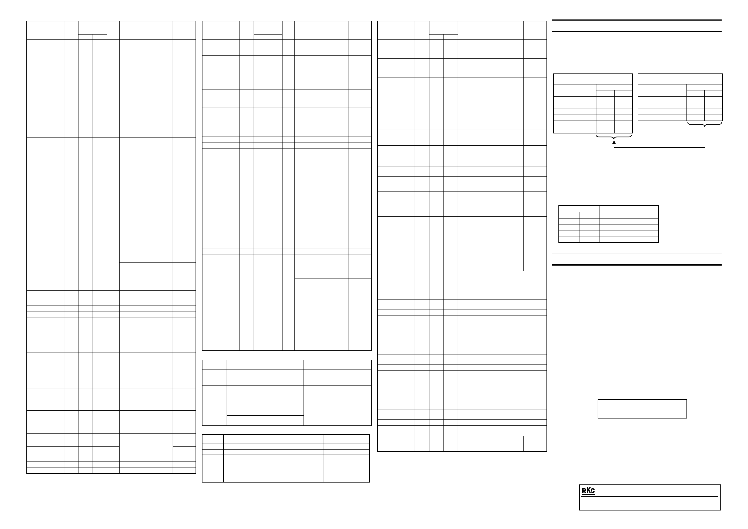
In this communication, it is possible to continuously read/write data by freely specifying 16
sets of data.
Register address to specify mapping data: 1000H to 100FH
Register address to actually read/write data: 1500H to 150FH
Register address of data which can be mapped: See 4. COMMUNICATION DATA LIST.
Example: When mapping Measured value (PV), Alarm 1 state monitor, Alarm 2 state monitor
and Alarm output state monitor to the register addresses from 1500H to 1503H
For data mapping
Factory set value: (−1: No mapping)
Name
Register address Register address
HEX DEC
Mapping data
Name
Setting 1 (For 1500H) 1000 4096 Measured value (PV) 00E0 224
Setting 2 (For 1501H) 1001 4097 Alarm 1 state monitor 00E2 226
Setting 3 (For 1502H) 1002 4098 Alarm 2 state monitor 00E3 227
Setting 4 (For 1503H) 1003 4099 Alarm output state monitor 00EC 236
•
•
•
Setting 16 (For 150FH) 100F 4111
•
•
•
•
•
•
Write to 1000H to 1003H.
1. The register address, “00E0H” of the “Measured value (PV)” to be mapped is written to
register address setting 1 (1000H).
2. The register address, “00E2H” of the “Alarm 1 state monitor” to be mapped is written to
register address setting 2 (1001H).
3. The register address, “00E3H” of the “Alarm 2 state monitor” to be mapped is written to
2
2
register address setting 3 (1002H).
4. The register address, “00ECH” of the “Alarm output state monitor” to be mapped is
written to register address setting 4 (1003H).
5. The assignment of the register addresses from 1500H to 1503H from/to which data is
actually read/written becomes as follows.
Register address
HEX DEC
1500 5376 Measured value (PV)
1501 5377 Alarm 1 state monitor
1502 5378 Alarm 2 state monitor
1503 5379 Alarm output state monitor
Name
High-speed communication
is performed by reading or
writing data in the
consecutive register
addresses from 1500H to
1503H.
6. COMMUNICATION SPECIFICATIONS
Interface: Based on RS-422A or RS-485, EIA standard
Synchronous method: Start-stop synchronous type
Communication speed: 1200 bps, 2400 bps, 4800 bps, 9600 bps, 19200 bps, 38400 bps
Data bit configuration: Start bit: 1
Connection method: RS-422A: 4-wire system, half-duplex multi-drop connection
RS-485: 2-wire system, half-duplex multi-drop connection
Protocol: • RKC communication (ANSI X3.28-1976 subcategory 2.5, A4)
Maximum connections: Up to 31 instruments
Termination resistor: Externally connected (Example: 120 Ω 1/2W)
Data mapping function: Up to 16 items (Only Modbus)
Interval time: 0 to 250 ms
Signal logic: RS-422A, RS-485
Data bit: RKC communication: 7 or 8
Modbus: 8
Parity bit: Without, Odd or Even
Stop bit: 1 or 2
Error control: Vertical parity (With parity bit selected)
Horizontal parity (BCC check)
Communication code: ASCII 7-bit code
Xon/Xoff control: None
• Modbus
Signal transmission mode:
Remote Terminal Unit (RTU) mode
Function code: 03H (Read holding registers)
06H (Preset single register)
08H (Diagnostics: loopback test)
10H (Preset multiple registers)
Error check method: CRC-16
Signal voltage Logic
V (A) − V (B) ≥ 2 V 0 (SPACE)
V (A) − V (B) ≤ −2 V 1 (MARK)
Voltage between V (A) and V (B) is the voltage
of (A) terminal for the (B) terminal.
Modbus is a registered tradema rk of Schneider Electric.
Company names and product names used i n this manual are the trademark s or registered
trademarks of the respective companies.
RKC INSTRUMENT INC.
®
HEADQUARTERS: 16-6, KUGAHARA 5-CHOME, OH TA-KU TOKYO 146-8515 JAPAN
PHONE: 03-3751-9799 (+81 3 3751 9799) E-mail: info@rk cinst.co.jp
FAX: 03-3751-8585 (+81 3 3751 8585) JAN. 2008
The first edition: OCT. 2007 [IMQ00]
The second edition: JAN. 2008 [IMQ00]
HEX DEC
 Loading...