

Preliminary
RT9907
3 Channel DC/DC Converters IC with
High-Efficiency Step-up and Step-down
General Description
The RT9907 is a three channel power-supply solution for
digital still cameras and other battery-powered devices. It
integrates an asynchronous step-up and two synchronous
step-down DC-DC converters. The RT9907 is targeted for
applications that use two AA cells or a single lithium-ion
battery.
The three DC-DC converters (CH1, CH2, CH3) accept input
voltage from 1.5V to 5.5V. Each DC-DC converter has
better transient response and excellent stability by
providing current-mode control and external compensation
network. With built-in Internal MOSFET and up to 1.4MHz
operating frequency, the RT9907 allows minimum BOM
cost and PCB area.
The step-down DC-DC converters (CH2, CH3) can regulate
output voltage as low as 0.8V. Three operational modes
are available: PWM, PSM, Low-Dropout modes. At PWM
mode, Internal synchronous rectifier with low R
dramatically reduces conduction loss and achieve 94%
efficiency. It enters Low-Dropout mode when normal PWM
cannot provide regulated output voltage by continuously
turning on the upper P-MOSFET. No external Schottky
diode is required in practical application.
Each DC-DC converter has independent enable input and
soft-start function allowing versatile power sequence
combination. Complete protection functions are
implemented such as short circuit, over-voltage protection.
DS(ON)
Features
zz
1.5V to 5.5V Battery Input Voltage Range
z
zz
zz
z Main step-up DC-DC Converter
zz
``
`1.5V to 5.5V Adjustable Output Voltage
``
``
`Up to 90% Efficiency
``
``
`2.6A, 0.3
``
zz
z T wo Step-Down DC-DC Converters
zz
``
`0.8V to 5.5V Adjustable Output Voltage
``
``
`94% Efficiency
``
``
`100% Duty Cycle
``
zz
z Up to 1.4MHz Switching Frequency
zz
μμ
zz
z 1
μA Supply Current in Shutdown Mode
zz
μμ
zz
z Programmable Soft Start Function
zz
zz
z Independent Enable Pin (CH1, CH2, CH3)
zz
zz
z External Compensation Network (CH1, CH2, CH3)
zz
zz
z Short Circuit Protection (CH1, CH2, CH3)
zz
zz
z Over Voltage Protection (CH2)
zz
zz
z 24-Lead VQFN Package
zz
zz
z RoHS Compliant and 100% Lead (Pb)-Free
zz
Ω Ω
Ω Internal Power Switch
Ω Ω
Applications
z Digital Still Camera
z PDAs
z Portable Device
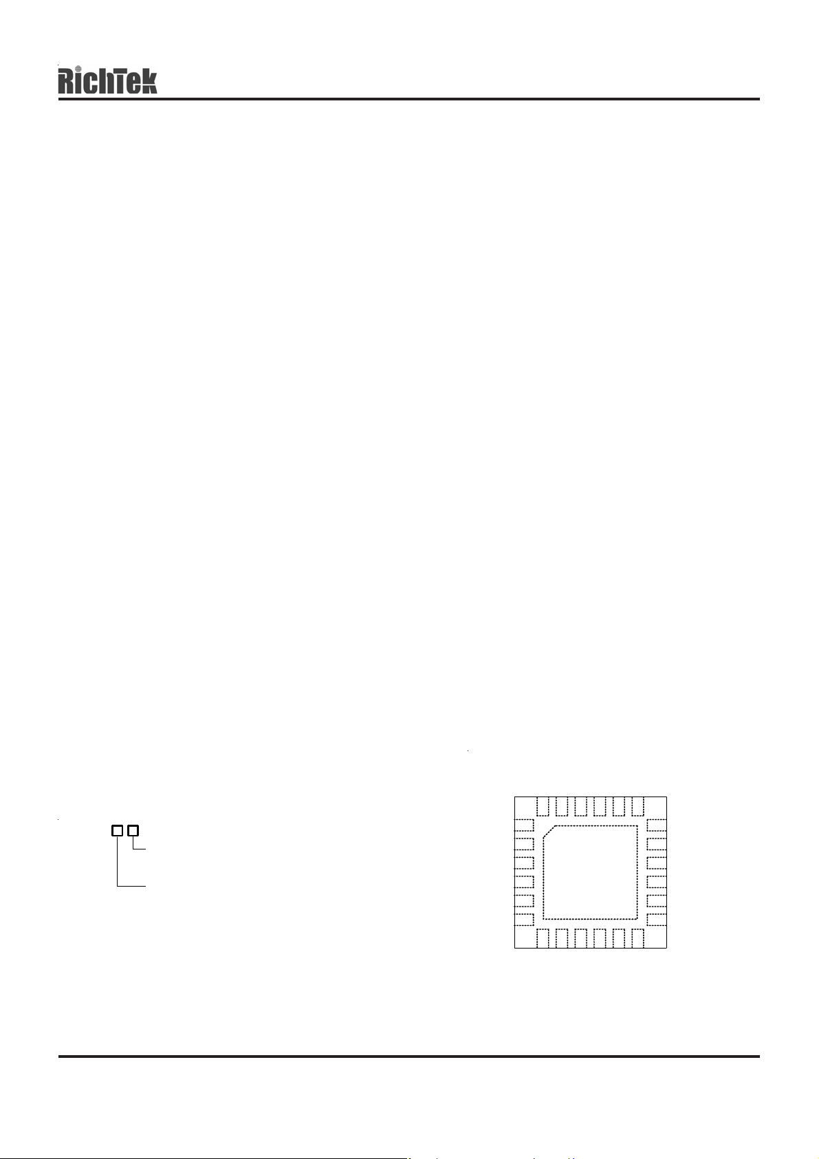
Pin Configurations
(TOP VIEW)
The RT9907 is available in small VQFN-24L 4x4 package.
COMP1 EN2
COMP2
FB2
18
EN1
17
ENM
16
VDD2
15
LX2
14
PGND2
13
LX1
11
VDD1
PGND1
FB3
GND
EN3
Ordering Information
RT9907
Package Type
QV : VQFN-24L 4x4 (V-Type)
Operating Temperature Range
P : Pb Free with Commercial Standard
Note :
RichTek Pb-free products are :
`RoHS compliant and compatible with the current require-
ments of IPC/JEDEC J-STD-020.
`Suitable for use in SnPb or Pb-free soldering processes.
COMP3
VDD3
LX3
PGND3
SS
RT
24 2223
1
2
3
4
5
6
7
GND
VQFN-24L 4x4
21 20 19
GND
8 9 10 12
FB1
VDDM
`100% matte tin (Sn) plating.
DS9907-03 November 2005 www.richtek.com
1
RT9907
Typical Application Circuit
1-cell Li+ Battery 3.4V to 4.2V
V
BAT
1.5V/500mA
10μF x 4
4.7nF
10μF x 2
200k
220k
Chip Enable
1nF
4.7μH
100pF
20k
10k
30k
1nF
1nF
Preliminary
V
BAT
2
VDD3
3
LX3
24
FB3
17
ENM
18
21
22
10
19
1
5
EN1
EN2
EN3
COMP1
COMP2
COMP3
SS
64
RT
RT9907
PGND3
14
10μF
8
VDDM
PGND2
PGND1
11 7 23
10μF
LX1
VDD1
FB1
VDD2
LX2
FB2
GND
GND
13
12
9
16
15
20
4.7μH
0.1μF
4.7μH
100pF
SS0520
680k
130k
150k
470k
5V/500mA
10μF x 4
V
10μF x 2
3.3V/500mA
10μF x 4
BAT
Figure 1. Typical Application Circuit for 1-cell Li+ Battery
DS9907-03 November 2005www.richtek.com
2
2-AA Battery 1.8V to 3.2V
V
BAT
1.5V/300mA
10μF x 4
4.7nF
10μF x 2
200k
220k
Chip Enable
1nF
4.7μH
100pF
20k
10k
30k
1nF
1nF
Preliminary
2
VDD3
3
LX3
24
FB3
17
ENM
18
EN1
21
EN2
22
EN3
10
COMP1
19
COMP2
1
COMP3
5
SS
RT
64
3.3V
8
VDDM
RT9907
PGND3
PGND2
11 7 23
14
10μF
LX1
VDD1
FB1
VDD2
LX2
FB2
GND
PGND1
GND
13
12
9
16
15
20
SS0520
470k
150k
4.7μH
100pF
4.7μH
220k
10μF x 2
10μF x 4
10μF x 2
470k
RT9907
V
BAT
I/O 3.3V/500mA
3.3V
2.5V/300mA
10μF x 4
Figure 2. Typical Application Circuit for 2-AA Battery Supply
DS9907-03 November 2005 www.richtek.com
3
RT9907
Function Block Diagram
Preliminary
VDDM ENM
SS
RT
Soft-Start
OSC
PWM
OSC
Thermal
Shutdown
CH1
Current-MODE
Asynchronous
Step-Up
PWM
Boost
CH2
Current-MODE
Synchronous
Step-Down
PWM
Buck2
CH3
Current-MODE
Synchronous
Step-Down
PWM
Buck3
EN
EN1
VDD1
LX1
PGND1
COMP1
FB1
EN2
VDD2
LX2
PGND2
COMP2
FB2
EN3
VDD3
LX3
PGND3
COMP3
FB3
GND
ENM EN1 EN2 EN3 CH1 CH2 CH3
0 X X X Off Off Off
1 0 0 0 Off Off Off
1 1 0 0 On Off Off
1 1 1 0 On On Off
1 1 1 1 On On On
DS9907-03 November 2005www.richtek.com
4

Functional Pin Description
Pin Number Pin Name Pin Function
Preliminary
RT9907
1 COMP3
2 VDD3
3 LX3
4 PGND3
5 SS
6 RT
7, 23
8 VDDM
9 FB1
10 COMP1
11 PGND1
12 VDD1
13 LX1
14 PGND2
15 LX2
16 VDD2
17 ENM
18 EN1
19 COMP2
GND
CH3 Feedback Compensation Pin.
CH3 Power Input Pin.
CH3 Switch Node. Drains of the internal P-Channel and N-Channel MOSFET switches.
Connect an inductor to LX3 pins together as close as possible.
Power Ground for CH3.
Sets the Soft Start interval of the converter. Connect a capacitor from this pin to ground.
Frequency setting resistor connection pin. Frequency is 500KHz if RT pin not connected
Analog Ground
Device Input Power Pin.
CH1 Feedback Input Pin.
CH1 Feedback Compensation Pin.
Power Ground for CH1
CH1 Power Input Pin. Connect output of Boost to this pin.
CH1 Switch Vode. Connect an inductor to LX1 Pins together as close as possible.
Power Ground for CH2.
CH2 Switch Node. Drains of the internal P-Channel and N-Channel MOSFET switches.
Connect an inductor to LX2 pins together as close as possible.
CH2 Power Input Pin.
Whole Device Control Pin. Tie this pin higher than 1.3V to enable the device. Tie below
0.4V to turn off the device.
CH1 Enable Input. Tie this pin higher than 1.3V to enable CH1. Tie below 0.4V to turn off
the CH1.
CH2 Feedback Compensation Pin.
20 FB2
21 EN2
22 EN3
24 FB3
Exposed Pad GND
DS9907-03 November 2005 www.richtek.com
CH2 Feedback Input.
CH2 Enable Input. Tie this pin higher than 1.3V to enable CH2. Tie below 0.4V to turn off
the CH2.
CH3 Enable Input. Tie this pin higher than 1.3V to enable CH3. Tie below 0.4V to turn off
the CH3.
CH3 Feedback Input.
Exposed pad should be soldered to PCB board and connected to GND.
5

RT9907
Preliminary
Absolute Maximum Ratings (Note 1)
z Supply Input Voltage, V
z LX1 Pin Switch Voltage ------------------------------------------------------------------------------------------ −0.3V to 7V
z LX2 Pin Switch Voltage ------------------------------------------------------------------------------------------ −0.3V to (V
z LX3 Pin Switch Voltage ------------------------------------------------------------------------------------------ −0.3V to (V
z Other I/O Pin Voltage ---------------------------------------------------------------------------------------------
z Power Dissipation, P
, V
DDM
DD1
@ TA = 25°C
D
, V
DD2,VDD3
------------------------------------------------------------------------------------------
−0.3 to 7V
−0.3V to (V
DD2
DD3
DDM
+ 0.3V)
+ 0.3V)
+ 0.3V)
VQFN-24L 4x4 ----------------------------------------------------------------------------------------------------- 1.85W
z Package Thermal Resistance (Note 3)
VQFN-24L 4x4, θJA------------------------------------------------------------------------------------------------ 54°C/W
z Junction Temperature Range------------------------------------------------------------------------------------ 0°C to 125°C
z Lead Temperature (Soldering, 10 sec.)----------------------------------------------------------------------- 260°C
z Operation Temperature Range ---------------------------------------------------------------------------------- −40°C to 85°C
z Storage Temperature Range ------------------------------------------------------------------------------------ −65°C to 150°C
z ESD Susceptibility (Note 2)
HBM (Human Body Mode) -------------------------------------------------------------------------------------- 2kV
MM (Machine Mode) ---------------------------------------------------------------------------------------------- 200V
Electrical Characteristics
(V
=3.3V, TA = 25°C, Unless Otherwise specification)
DDM
Parameter Symbol Test Condition Min Typ Max Units
Supply Voltage
Minimum Startup Voltage (Boost) VST Boost loading < 1mA -- 1.5 -- V
VDDM Operating Voltage V
VDD1, VDD2, VDD3 Operating
Volta ge
V
V
V
VDDM Over Voltage Protection -- 6.5 -- V
Supply Current
Shutdown Supply Current I
CH1 DC/DC Converter I
CH2 DC/DC Converter Supply
Current
CH3 DC/DC Converter Supply
Current
I
I
VDDM Pin Voltage 2.4 -- 5.5 V
VDDM
VDD1
VDD2
VDD3
OFF
VDDM
VDDM
VDDM
VDD1, VDD2, VDD3 Pin
,
Voltage 1.5 5.5 V
V
pin=0V -- 0.01 1 μA
ENM
= 3.3V,
V
VDDM
V
= 0.9V
FB1
V
ENM
V
EN2
V
VDDM
V
FB2
V
ENM
V
EN2
V
VDDM
V
FB3
V
ENM
V
EN2
= 3.3V, V
= 0V, V
= 3.3V,
= 0.9V
= 3.3V, V
= 3.3V, V
= 3.3V,
= 0.9V
= 3.3V, V
= 0V, V
EN1
EN3
EN1
EN3
EN1
EN3
= 3.3V,
= 0V
= 0V,
= 0V
= 0V,
= 3.3V
-- 250 350 μA
-- 250 350 μA
-- 250 350 μA
To be continued
DS9907-03 November 2005www.richtek.com
6

Preliminary
RT9907
Parameter Symbol Test Condition Min Typ Max Units
Oscillator
Operation Frequency Range F
CH1 Maximum Duty Cycle D
CH2 Maximum Duty Cycle D
CH3 Maximum Duty Cycle D
RT Open 475 550 625 kHz
OSC
-- 85 90 %
MAX1
-- -- 100 %
MAX2
-- -- 100 %
MAX3
Feedback Voltage (CH1, CH2, CH3)
Feedback Voltage VFB CH1, CH2, CH3 0.788 0.8 0.812 V
Feedback Voltage ︱ΔVFB︱
CH1, CH2, CH3
3.0V < V
DDM
< 5.5V
-- -- 12
mV
Error Amplifier
GM -- 0.2 -- ms
Compensation Source Current -- 22 -- μA
Compensation Sink Current -- 22 -- μA
Power Switch
CH1 On Resistance of MOSFET R
CH1 Current Limitation V
CH2 On Resistance of MOSFET R
N-MOSFET -- 300 400 mΩ
DS(ON)
= 3.3V 2 2.6 3 A
VDD1
DS(ON)
N-MOSFET, V
P-MOSFET, V
= 3.3V -- 350 450 mΩ
VDD2
= 3.3V -- 350 450 mΩ
VDD2
CH2 Current Limitation V
CH3 On Resistance of MOSFET R
DS(ON)
CH3 Current Limitation V
= 3.3V 1.3 1.5 1.9 A
VDD2
N-MOSFET, V
P-MOSFET, V
= 3.3V 1.3 1.5 1.9 A
VDD3
= 3.3V -- 350 450 mΩ
VDD3
= 3.3V -- 350 450 mΩ
VDD3
UVP (CH2, CH3) & Over Voltage Protection (CH2)
UVP Threshold Voltage @FB2, FB3 0.3 0.4 0.5 V
Over Voltage Protection @FB2 0.95 1 -- V
Control
ENM, EN1, EN2, EN3 Input High
Level Threshold
ENM, EN1, EN2, EN3 Input Low
Level Threshold
= 3.3V -- 0.8 1.3 V
V
VDDM
V
= 3.3V 0.4 0.8 -- V
VDDM
Thermal Protection
Thermal Shutdown TSD 140 180 -- °C
Thermal Shutdown Hysteresis ΔTSD -- 10 -- °C
Note 1. Stresses listed as the above "Absolute Maximum Ratings" may cause permanent damage to the device. These are for
stress ratings. Functional operation of the device at these or any other conditions beyond those indicated in the
operational sections of the specifications is not implied. Exposure to absolute maximum rating conditions for extended
periods may remain possibility to affect device reliability.
Note 2. Devices are ESD sensitive. Handling precaution recommended.
Note 3. θ
is measured in the natural convection at TA = 25°C on a low effective thermal conductivity test board of
JA
JEDEC 51-3 thermal measurement standard.
DS9907-03 November 2005 www.richtek.com
7

RT9907
Typical Operating Characteristics
Preliminary
Reference Voltage vs. Temperature
0.808
0.806
0.804
0.802
0.8
0.798
0.796
Reference Voltage (V)
0.794
0.792
-50-30-10103050 7090
Temperature
(°C)
Boost Efficiency vs. Output Current
100
V
= 3.3V
OUT
90
80
70
Efficiency (%)
60
50
1 10 100 1000
Output Current (mA)
V
3V
2.5V
2V
1.8V
Boost
Oscillator Ferquency vs. R
1800
1600
1400
1200
1000
800
600
400
Oscillator Frequecny (kHz)
200
0
0 100 200 300 400 500 600
RT
RRT (kΩ)
Boost Output Voltage vs. V
3.345
IN
3.335
3.325
3.315
Output Voltage (V)
3.305
V
= 2.5V, V
3.34
3.33
3.32
3.31
BAT
1.5 2 2.5 3 3.5 4 4.5 5 5.5
DDM
= 3.3V, I
V
Voltage (V)
DD1
OUT
= 250mA
DD1
Voltage
Boost Output Voltage v s . V
3.332
V
= 2.5V, V
BAT
3.33
3.328
3.326
3.324
3.322
Output Voltage (V)
3.32
3.318
3.316
2.42.83.23.6 4 4.44.85.25.6
= 3.3V, I
DD1
V
Voltage (V)
DDM
OUT
= 250mA
DDM
Voltage
Deviation
Output Voltage
Load Current
Boost Load T ransient Respon se
(100mV/Div)
VIN = 1.8V, V
(200mA/Div)
= 3.3V, @I
OUT
Time (1ms/Div)
OUT
= 100mA to 400mA
DS9907-03 November 2005www.richtek.com
8

Preliminary
RT9907
Deviation
(100mV/Div)
Output Voltage
(200mA/Div)
Load Current
Deviation
(100mV/Div)
Output Voltage
Boost Load Transient Response
VIN = 2V, V
= 3.3V, @I
OUT
Time (1ms/Div)
= 100mA to 400mA
OUT
Boost Load Transient Response
Deviation
Output Voltage
Load Current
1
LX
(2V/Div)
Boost Load Transient Response
(100mV/Div)
(200mA/Div)
VIN = 2.5V, V
= 3.3V, @I
OUT
OUT
Time (1ms/Div)
Boost LX & Output Ripple
VIN = 1.8V, V
= 3.3V, @I
OUT
OUT
= 100mA to 400mA
= 100mA
(200mA/Div)
Load Current
1
LX
(2V/Div)
(10mV/Div)
Output Ripple
VIN = 3V, V
VIN = 1.8V, V
= 3.3V, @I
OUT
= 100mA to 400mA
OUT
Time (1ms/Div)
Boost LX & Output Ripple
= 3.3V, @I
OUT
Time (1us/Div)
= 300mA
OUT
(10mV/Div)
Output Ripple
1
LX
(2V/Div)
(10mV/Div)
Output Ripple
Time (1us/Div)
Boost LX & Output Ripple
VIN = 2.5V, V
= 3.3V, @I
OUT
Time (1us/Div)
= 100mA
OUT
DS9907-03 November 2005 www.richtek.com
9

RT9907
Preliminary
1
LX
(2V/Div)
(10mV/Div)
Output Ripple
1
LX
(2V/Div)
Boost LX & Output Ripple
VIN = 2.5V, V
= 3.3V, @I
OUT
Time (1us/Div)
Boost LX & Output Ripple
VIN = 3V, V
= 3.3V, @I
OUT
OUT
= 400mA
OUT
= 400mA
1
LX
(2V/Div)
(10mV/Div)
Output Ripple
100
90
80
70
Efficiency (%)
Boost LX & Output Ripple
VIN = 3V, V
= 3.3V, @I
OUT
= 100mA
OUT
Time (1us/Div)
Buck2 Efficiency vs. Output Current
V
= 1.5V
OUT
V
2.2V
IN =
V
= 4.5V
IN
V
V
= 3.8V
IN
IN
= 3V
V
IN =
2.5V
(10mV/Div)
Output Ripple
Time (1us/Div)
Buck2 Efficiency vs. Output Current
100
V
= 1.8V
OUT
90
80
V
70
Efficiency (%)
60
50
1 10 100 1000
V
2.5V
IN =
V
= 3.8V
IN
= 4.5
IN
Output Current (mA)
V
IN
= 3V
60
50
1 10 100 1000
Output Current (mA)
Buck2 Efficiency vs. Output Current
100
V
= 2.5V
OUT
90
V
= 4.5
80
70
60
Efficiency (%)
50
40
30
1 10 100 1000
V
= 3.8V
IN
V
= 3V
IN
IN
Output Current (mA)
10
DS9907-03 November 2005www.richtek.com

Preliminary
RT9907
Buck2 Output Voltage vs. V
1.82
V
= V
DDM
= 3.3V, I
BAT
1.81
2 2.5 3 3.5 4 4.5
Output Voltage (V)
1.818
1.816
1.814
1.812
1.808
1.806
1.804
OUT
V
Voltage (V)
DD2
= 250mA
Buck2 Load Transient Response
@I
= 100mA to 400mA
OUT
DD2
Volta ge
Output Voltage (V)
Buck2 Output Voltage vs. V
1.82
V
= 3.3V, I
1.818
1.816
1.814
1.812
1.808
1.806
1.804
DD2
1.81
2 2.5 3 3.5 4 4.5 5 5.5 6
OUT
V
= 250mA
Voltage (V)
DDM
DDM
Buck2 Load Transient Response
@I
= 100mA to 400mA
OUT
Voltage
Deviation
Output Voltage
Load Current
Deviation
Output Voltage
(100mV/Div)
V
= 2.5V, V
DD2
(200mA/Div)
DDM
= 3.3V, V
OUT
Time (1ms/Div)
Buck2 Load Transient Response
@I
= 100mA to 400mA
OUT
(100mV/Div)
= 1.8V
Deviation
Output Voltage
Load Current
Deviation
Output Voltage
(100mV/Div)
V
= 3V, V
DD2
(200mA/Div)
DDM
= 3.3V, V
OUT
= 1.8V
Time (1ms/Div)
Buck2 Load Transient Response
@I
= 100mA to 400mA
OUT
(100mV/Div)
V
(200mA/Div)
Load Current
= 3.8V, V
DD2
= 3.3V, V
DDM
Time (1ms/Div)
OUT
= 1.8V
(200mA/Div)
Load Current
= 4.5V, V
DD2
= 3.3V, V
DDM
Time (1ms/Div)
OUT
= 1.8V
V
DS9907-03 November 2005 www.richtek.com
11

RT9907
Preliminary
2
LX
(2V/Div)
(10mV/Div)
Output Ripple
2
LX
(2V/Div)
Buck2 LX & Output Ripple
@I
= 500mA
OUT
V
= 2.5V, V
DD2
= 3.3V, V
DDM
Time (500ns/Div)
Buck2 LX & Output Ripple
OUT
= 1.8V
2
LX
(2V/Div)
(10mV/Div)
Output Ripple
2
LX
(2V/Div)
Buck2 LX & Output Ripple
@I
= 250mA
OUT
V
= 2.5V, V
DD2
= 3.3V, V
DDM
Time (500ns/Div)
Buck2 LX & Output Ripple
OUT
= 1.8V
(10mV/Div)
Output Ripple
2
LX
(2V/Div)
(10mV/Div)
Output Ripple
@I
= 250mA
OUT
V
DD2
= 3V, V
DDM
= 3.3V, V
OUT
Time (500ns/Div)
Buck2 LX & Output Ripple
@I
= 250mA
OUT
V
= 3.8V, V
DD2
= 3.3V, V
DDM
Time (500ns/Div)
= 1.8V
OUT
= 1.8V
(10mV/Div)
Output Ripple
2
LX
(2V/Div)
(10mV/Div)
Output Ripple
@I
= 500mA
OUT
V
DD2
= 3V, V
= 3.3V, V
DDM
OUT
Time (500ns/Div)
Buck2 LX & Output Ripple
@I
= 500mA
OUT
V
= 3.8V, V
DD2
= 3.3V, V
DDM
Time (500ns/Div)
= 1.8V
OUT
= 1.8V
12
DS9907-03 November 2005www.richtek.com

Preliminary
RT9907
2
LX
(2V/Div)
(10mV/Div)
Output Ripple
100
90
80
70
Efficiency (%)
Buck2 LX & Output Ripple
@I
= 250mA
OUT
V
= 4.5V, V
DD2
= 3.3V, V
DDM
OUT
= 1.8V
Time (500ns/Div)
Buck3 Efficiency vs. Output Current
V
= 1.5V
OUT
V
IN
= 4.5V
V
IN
= 3.8V
V
2.2V
IN =
V
2.5V
= 3V
IN =
V
IN
2
LX
(2V/Div)
(10mV/Div)
Output Ripple
100
90
80
70
Efficiency (%)
Buck2 LX & Output Ripple
@I
= 500mA
OUT
V
= 4.5V, V
DD2
= 3.3V, V
DDM
OUT
= 1.8V
Time (500ns/Div)
Buck3 Efficiency vs. Output Current
V
= 1.8V
OUT
V
= 4.5V
IN
V
= 3.8V
IN
V
IN =
2.5V
V
IN
= 3V
60
50
1 10 100 1000
Output Current (mA)
Buck3 Efficiency vs. Output Current
100
V
= 2.5V
OUT
90
V
= 4.5V
80
70
V
IN
IN
= 3V
60
Efficiency (%)
50
40
30
V
1 10 100 1000
IN
= 3.8V
Output Current (mA)
Output Voltage (V)
60
50
1 10 100 1000
Output Current (mA)
Buck3 Output Voltage vs. V
1.806
V
= V
DDM
= 3.3V, I
BAT
1.804
1.802
1.8
1.798
1.796
1.794
1.792
1.79
2 2.5 3 3.5 4 4.5
V
= 250mA
OUT
Voltage (V)
DD3
DD3
Voltage
DS9907-03 November 2005 www.richtek.com
13

RT9907
Preliminary
1.806
1.804
1.802
1.8
1.798
1.796
1.794
Output Voltage (V)
1.792
1.79
Deviation
(100mV/Div)
Output Voltage
Buck3 Output Voltage vs. V
V
= 3.3V, I
DD3
2 2.5 3 3.5 4 4.5 5 5.5 6
OUT
V
= 250mA
Voltage (V)
DDM
DDM
Voltage
Buck3 Load Transient Response
@I
= 100mA to 400mA
OUT
Deviation
Output Voltage
Load Current
Deviation
Output Voltage
Buck3 Load Transient Response
@I
= 100mA to 400mA
OUT
(100mV/Div)
V
= 2.5V, V
DD3
DDM
= 3.3V, V
OUT
(200mA/Div)
Time (1ms/Div)
Buck3 Load Transient Response
@I
= 100mA to 400mA
OUT
(100mV/Div)
= 1.8V
14
Load Current
Deviation
Output Voltage
Load Current
V
= 3V, V
DD3
(200mA/Div)
Buck3 Load Transient Response
@I
OUT
(100mV/Div)
V
= 4.5V, V
DD3
(200mA/Div)
= 3.3V, V
DDM
Time (1ms/Div)
= 100mA to 400mA
= 3.3V, V
DDM
Time (1ms/Div)
OUT
= 1.8V
OUT
= 1.8V
(200mA/Div)
Load Current
3
LX
(2V/Div)
(10mV/Div)
Output Ripple
V
= 3.8V, V
DD3
DDM
= 3.3V, V
Time (1ms/Div)
Buck3 LX & Output Ripple
@I
= 250mA
OUT
V
= 2.5V, V
DD3
= 3.3V, V
DDM
Time (500ns/Div)
DS9907-03 November 2005www.richtek.com
OUT
OUT
= 1.8V
= 1.8V

Preliminary
RT9907
3
LX
(2V/Div)
(10mV/Div)
Output Ripple
3
LX
(2V/Div)
Buck3 LX & Output Ripple
@I
= 500mA
OUT
V
= 2.5V, V
DD3
= 3.3V, V
DDM
Time (500ns/Div)
Buck3 LX & Output Ripple
@I
= 500mA
OUT
OUT
= 1.8V
3
LX
(2V/Div)
(10mV/Div)
Output Ripple
3
LX
(2V/Div)
Buck3 LX & Output Ripple
@I
= 250mA
OUT
V
DD3
= 3V, V
DDM
= 3.3V, V
OUT
Time (500ns/Div)
Buck3 LX & Output Ripple
@I
= 250mA
OUT
= 1.8V
(10mV/Div)
Output Ripple
3
LX
(2V/Div)
(10mV/Div)
Output Ripple
V
DD3
= 3V, V
= 3.3V, V
DDM
OUT
Time (500ns/Div)
Buck3 LX & Output Ripple
@I
= 500mA
OUT
V
= 3.8V, V
DD3
= 3.3V, V
DDM
Time (500ns/Div)
= 1.8V
= 1.8V
OUT
(10mV/Div)
Output Ripple
3
LX
(2V/Div)
(10mV/Div)
Output Ripple
V
= 3.8V, V
DD3
= 3.3V, V
DDM
Time (500ns/Div)
Buck3 LX & Output Ripple
@I
= 250mA
OUT
V
= 4.5V, V
DD2
= 3.3V, V
DDM
Time (500ns/Div)
OUT
OUT
= 1.8V
= 1.8V
DS9907-03 November 2005 www.richtek.com
15

RT9907
3
LX
(2V/Div)
(10mV/Div)
Output Ripple
V
DD2
Buck3 LX & Output Ripple
@I
= 500mA
OUT
= 4.5V, V
= 3.3V, V
DDM
OUT
Time (500ns/Div)
= 1.8V
Preliminary
16
DS9907-03 November 2005www.richtek.com

Application Information
Preliminary
RT9907
The RT9907 is a three-channel DC/DC converter with one
voltage detector for digital still cameras and other hand-
held device. The three channels DC/DC converters are as
follows:
CH1: Step-up, asynchronous current mode DC/DC
converter with an internal power MOSFET, current limit
protection and high efficiency control for wide loading
range
CH2: Step-down, synchronous current mode DC/DC
converter with internal power MOSFETs, current limit,
short-circuit , over voltage protection and high efficiency
control for wide loading range.
CH3: Step-down, synchronous current mode DC/DC
converter with internal power MOSFETs, current limit,
short-circuit protection and high efficiency control for wide
loading range.
Soft-Start
CH1, CH2 and CH3 can be soft-started individually every
time when the channel is enabled. Soft-start is achieved
by ramping up the voltage reference of each channel's
input of error amplifier. Adding a capacitor on SS pin to
ground sets the ramping up speed of each voltage
reference. Triangle wave will be appeared on SS pin,
which provides a clock base for soft-start.
The soft-start timing would be setted by following formular.
C
SS
(ms)
x 10 T
=
SS
Oscillator
The internal oscillator synchronizes CH1, CH2 and CH3
PWM operation frequency. The operation frequency is
set by a resistor between RT pin to ground, ranging from
550kHz to 1.4MHz.
Step-up (Boost) DC/DC Converter (CH1)
The step-up channel (CH1) is designed as current-mode
DC/DC PWM converters with built-in internal power MOS
and external Schottky diode. Output voltage is regulated
and adjustable up to 5.5V. This channel typically supplies
3.3V for main system power.
At light load, efficiency is enhanced by pulse-skipping
1nF
mode. In this mode, the NMOS turns on by a constant
pulse width. As loading increased, the converter operates
at constant frequency PWM mode. The max. duty of the
constant frequency is 80% for the boost to prevent high
input current drawn from input.
Protection
Current limit
The current of NMOS is sensed cycle by cycle to prevent
over current. If the current is higher than 2.6A (typical),
then the NMOS is off . This state is latched and then
reset automatically at next clock cycle.
Under Voltage
The status of under voltage is decided by comparing FB1
voltage with 0.4V. This function is enabled after soft start
finishes. If the FB1 voltage is less than 0.4V, then the
NMOS will be turned off immediately. And this state is
latched. After a dummy count period, the controller begins
a re-soft-start procedure.
If the status of under voltage remains after 4 successive
times of soft-start, then CH1 is latched.
Over Voltage
The over voltage protection is used when the output of
CH1 supplies the power of the main chip. If the output
voltage of CH1 is over 6.5V, the main chip is shutdown
and the NMOS is kept off.
Step-Down (Buck) DC/DC Converter (CH2, CH3)
The step-down channels (CH2, CH3) are designed as
synchronous current-mode DC/DC PWM converters.
Output voltage is regulated and adjustable down to 0.8V.
The internal synchronous power switches eliminate the
typical Schottky free wheeling diode and improve
efficiency.
At light load, efficiency is enhanced by pulse-skipping
mode. In this mode, the high-side PMOS turns on by a
constant pulse width. As loading increased, the converter
operates at constant frequency PWM mode. While the
input voltage is close to output voltage, the converter
enters low dropout mode. Duty could be as long as 100%
to extend battery life.
DS9907-03 November 2005 www.richtek.com
17

RT9907
Preliminary
Protection
Current limit (CH2, CH3)
The current of high-side PMOS is sensed cycle by cycle
to prevent over current. If the current is higher than 1.5A
(typical), then the high-side PMOS is off and the low-side
NMOS is on. This state is latched and then reset
automatically at next clock cycle.
Under Voltage (CH2, CH3)
The status of under voltage is decided by comparing FB2
(or FB3) voltage with 0.4V. This function is enabled after
soft start finishes. If the FB2 (or FB3) voltage is less than
0.4V, then the high/low-side Power MOS are turned off
immediately. And this state is latched. After a dummy
count period, the CH2 (or CH3) begins a soft-start
procedure.
However, if the status of under voltage remains after 3
successive times of soft-start, then CH2 (or CH3) is
latched.
Thermal Protection
Thermal protection function is integrated in the chip. When
the chip temperature is higher than 178 degree C, the
controllers of CH1, CH2, and CH3 are shutdown. 10 degree
C is the hysteresis range of temperature to prevent unstable
operation when the thermal protection happens. When the
thermal protection is relieved, the chip operates well again.
UV remain after 3
successive soft-start
CH2 CH2 is latched, and whole
IC is shut down
CH3 CH3 is latched Toggle EN3 or ENM
Over Voltage Protection (CH2)
Over voltage protection (OVP) is used to protect the
external parts connected to the output of CH2. If the FB2
voltage is higher than 1V, the high-side PMOS is off and
low-side NMOS is on. This status is latched and could be
reset by toggling ENM.
Reference
The chip has an internal 0.8V reference voltage, which is
the inputs of the error amplifiers of the CH1, CH2, and CH3
to compare the difference of feedback voltage. The
reference voltage can be set up stably when the supplied
power (VDDM) is above 1.5V, and EN1 (or EN2, EN3) goes
high.
How to reset?
Toggle ENM
18
DS9907-03 November 2005www.richtek.com

Outline Dimension
Preliminary
RT9907
D
E
A
A3
A1
D2
SEE DETAIL A
1
be
E2
L
1
2
1
2
DETAIL A
Pin #1 ID and Tie Bar Mark Options
Note : The configuration of the Pin #1 identifier is optional,
but must be located within the zone indicated.
Dimensions In Millimeters Dimensions In Inches
Symbol
Min Max Min Max
A 0.800 1.000 0.031 0.039
A1 0.000 0.050 0.000 0.002
A3 0.175 0.250 0.007 0.010
b 0.180 0.300 0.007 0.012
D 3.950 4.050 0.156 0.159
D2 2.300 2.750 0.091 0.108
E 3.950 4.050 0.156 0.159
E2 2.300 2.750 0.091 0.108
e 0.500 0.020
L 0.350 0.450
RICHTEK TECHNOLOGY CORP.
Headquarter
5F, No. 20, Taiyuen Street, Chupei City
Hsinchu, Taiwan, R.O.C.
Tel: (8863)5526789 Fax: (8863)5526611
0.014 0.018
V-Type 24L QFN 4x4 Package
RICHTEK TECHNOLOGY CORP.
Taipei Office (Marketing)
8F-1, No. 137, Lane 235, Paochiao Road, Hsintien City
Taipei County, Taiwan, R.O.C.
Tel: (8862)89191466 Fax: (8862)89191465
Email: marketing@richtek.com
DS9907-03 November 2005 www.richtek.com
19

 Loading...