

Preliminary
RT9903
5 Channel DC/DC Converters IC
with High-Efficiency Step-up
General Description
The RT9903 is a complete power-supply solution for digital
still cameras and other hand-held devices. It integrates a
high-efficiency fours step-up DC-DC converte
rs and a
charge pump.
The two Step-up DC-DC converters (CH1,CH2) accept
inputs from 1.5V to 5.5V and regulate a resistor-
adjustable output up to 17V. One Step-up DC-DC
converter (CH3) can be regarded as white LED Driver,
which reference voltage is 0.2V and have OVP function.
One step-up DC-DC converter (CH4) regulate a resistor-
adjustable output up 5V. An adjustable operating
frequency (up to 1.4MHz) is utilized to get optimum size,
cost, and efficiency.
The feature of the charge pump (CH5) is to deliver few
current to CCD negative voltage.
RT9903 is available in VQFN-24L 4x4 package. Each
DC-DC converters have independent shutdown inputs.
Applications
z Digital Still Camera
z PDAs
z Portable Device
Features
zz
T wo step-up DC-DC Converters (CH1, CH2)
z
zz
``
`HV Internal Switches
``
``
`50mA Load Current
``
zz
z One Step-up DC-DC Converter (CH3)
zz
``
`0.2V Reference Voltage
``
``
`HV Internal Switches
``
``
`LED Brightness Dimming Control
``
``
`Over Voltage Protection
``
zz
z One Step-up DC-DC Converter (CH4)
zz
``
`External Switches
``
``
`External Current Limit Setting
``
zz
z Step-up Charge Pump (CH5) for CCD Negative
zz
Voltage
``
`HV Internal Switches
``
zz
z Up to 1.4MHz Switching Frequency
zz
μμ
zz
z 1
μA Supply Current in Shutdown Mode
zz
μμ
zz
z External Compensation Network for All Converters
zz
zz
z Programm able Soft Start Function (CH1, CH2, CH3,
zz
CH4)
zz
z Independent Ena ble Pin to Shutdown Each Channel
zz
zz
z 24-Lead VQFN Package
zz
zz
z RoHS Compliant and 100% Lead (Pb)-Free
zz
Pin Configurations
Ordering Information
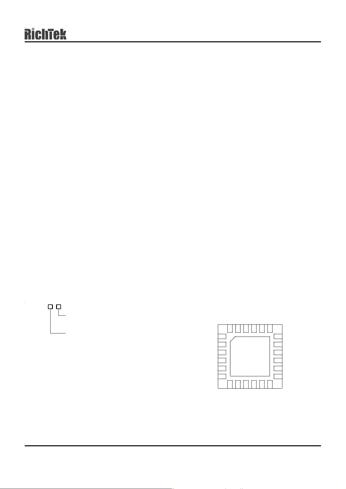
(TOP VIEW)
RT9903
Package Type
QV : VQFN-24L 4x4 (V-Type)
Operating Temperature Range
P : Pb Free with Commercial Standard
Note :
RichTek Pb-free products are :
`RoHS compliant and compatible with the current require-
ments of IPC/JEDEC J-STD-020.
`Suitable for use in SnPb or Pb-free soldering processes.
`100% matte tin (Sn) plating.
Marking Information
For marking information, contact our sales representative
CX
INCD
FB_CP
RT
EXT4
CS4
LX2
COMP2
24 2223
1
2
3
4
5
6
7
8910 12
FB4
COMP4
VQFN-24L 4x4
FB2
21 20 19
GND
FB3
11
COMP3 AGND
FB1
LX3
COMP1
18
LX1
17
VDD
16
PGND
15
EN4
14
EN2
13
EN1
EN3
directly or through a RichTek distributor located in your
area, otherwise visit our website for detail.
DS9903-04 November 2005 www.richtek.com
1
RT9903
Typical Application Circuit
2-AA Battery 1.8V to 3.2V
Preliminary
WLED
(12V)
3.3V_Motor
C5 to C8
10uFx4
VBATT
R15
R5
1.2k
C10
4.7nF
10
300k
130k
R2
R3
C11
500pF
C3
10uF10uF
SS0520
Chip Enable
R6
C12
6.8nF
C1
10uF
D1
SS0520
C2
1uF
C4
D2
C9
1nF
R7
C13
56nF
R1
VBATT
L2
4.7uH
Q1
Si2302
R8
2.7k1.2k2.2k
C14
4.7nF
L1
4.7uH
R4
10k
11
4
21
16
9
6
5
7
13
14
12
15
19
23
10
8
VDD
LX3
RT
AGND
PGND
FB3
CS4
EXT4
FB4
EN1
EN2
EN3
EN4
COMP1
COMP2
COMP3
COMP4
17
RT9903
C15
4.7uF
FB-CP
LX1
FB1
LX2
FB2
INCD
CX
18
20
24
22
2
1
3
C16
10uF
C24
68nF
VBATT
C19
10uF
L3
4.7uH
SS0520
L4
4.7uH
SS0520
SS0520
D6
SS0520
VCC
3.3V
D3
R9
2.2M
D4
R11
5.1M
R12
360k
D5
R10
200k
R13
750k
R14
330k
1uF
C27
C17
1nF
C21 to C23
10uFx3
C20
1nF
+12V (+LCD)
C18
10uF
+15V (+CCD)
-7.5V (-CCD)
C25 to C26
10uFx2
DS9903-04 November 2005www.richtek.com
2
WLED
(12V)
3.3V_Motor
C5 to C8
10uFx4
1.2k
4.7nF
VBATT
R15
10
R5
C10
R2
300k
R3
130k
C11
500pF
C2
1uF
C3
10uF10uF
SS0520
Chip Enable
R6
2.2k
C12
6.8nF
C1
10uF
D1
SS0520
C4
D2
C9
1nF
R7
1.2k
C13
56nF
R1
VBATT
L2
4.7uH
Q1
Si2302
R8
2.7k
C14
4.7nF
L1
4.7uH
R4
10k
11
4
21
16
9
6
5
7
13
14
12
15
19
23
10
8
Preliminary
V_3.3V
17
VDD
LX3
RT
AGND
PGND
FB3
RT9903
CS4
EXT4
FB4
EN1
EN2
EN3
EN4
COMP1
COMP2
COMP3
COMP4
C15
4.7uF
FB-CP
LX1
FB1
LX2
FB2
INCD
CX
18
20
24
22
2
1
3
C16
10uF
C24
68nF
C19
10uF
L3
4.7uH
VBATT
SS0520
VCC
3.3V
D3
SS0520
R9
2.2M
L4
4.7uH
D4
SS0520
R11
5.1M
R12
360k
D5
SS0520
D6
R10
200k
R13
750k
R14
330k
C27
1uF
C17
1nF
C20
1nF
+12V (+LCD)
C18
10uF
C21 to C23
10uFx3
C28
C25 to C26
10uFx2
RT9903
+15V (+CCD)
-7.5V (-CCD)
Function Block Diagram
CX
Charge Pump
Thermal
Protection
PGND (Exposed Pad)
Oscillator
+
-
RT
Soft
Start
VDD
AGND
COMP1
COMP3
EN1
CH1
V-Mode
Step-Up
PWM
CH3
C-Mode
Step-Up
PWM
EN3
LX1
LX3
-
FB3
+
+
V
FB1
V
REF
0.2V
REF
1V
COMP4
COMP2
LX2 FB2 FBCPINCD
EN2
CH2
V-Mode
Step-Up
PWM
CH4
C-Mode
Step-Up
PWM
10uA
CS4
EXT4
EN4
+
+
-
FB4
DS9903-04 November 2005 www.richtek.com
3

RT9903
Preliminary
Functional Pin Description
Pin Number Pin Name Pin Function
1 CX Charge Pump External Driver Pin
2 INCD Charge Pump Input Pin
3 FB_CP Charge Pump Feedback Pin
4 RT Frequency Setting Resistor Connection Pin
5 EXT4 CH4 External Power Switch
6 CS4 CH4 Current Sense Input Pin
7 FB4 CH4 Feedback Input
8 COMP4 CH4 Feedback Compensation Pin
9 FB3 CH3 Feedback Input
10 COMP3 CH3 Feedback Compensation Pin
11 LX3 CH3 Switch Node
12 EN3 CH3 Enable Input Pin
13 EN1 CH1 Enable Input Pin
14 EN2 CH2 Enable Input Pin
15 EN4 CH4 Enable Input Pin
16
17 VDD Power Input Pin
18 LX1 CH1 Switch Node
19 COMP1 CH1 Feedback Compensation Pin
20 FB1 CH1 Feedback Input
21 AGND Analog Ground
22 FB2 CH2 Feedback Input
23 COMP2 CH2 Feedback Compensation Pin
24 LX2 CH2 Switch Node
Exposed Pad GND Exposed pad should be soldered to PCB board and connected to GND.
PGND Power Ground
DS9903-04 November 2005www.richtek.com
4
Preliminary
Absolute Maximum Ratings (Note 1)
RT9903
z Supply Input Voltage (V
z LX1, LX2, LX3 Pins, INCD Pin---------------------------------------------------------------------------------------- −0.3V to 20V
z Other I/O Pin Voltage ---------------------------------------------------------------------------------------------------
z Power Dissipation, P
) --------------------------------------------------------------------------------------------- −0.3 to 7V
DD
@ T
D
= 25°C
A
−0.3V to 7V
VQFN-24L 4x4 ------------------------------------------------------------------------------------------------------------ 1.923W
z Package Thermal Resistance (Note 3)
VQFN-24L 4x4, θJA------------------------------------------------------------------------------------------------------- 52°C/W
z Lead Temperature (Soldering, 10 sec.) ---------------------------------------------------------------------------- 260°C
z Operation Temperature Range --------------------------------------------------------------------------------------- −40°C to 85°C
z Junction Temperature Range ----------------------------------------------------------------------------------------- 0°C to 125°C
z Storage Temperature Range ------------------------------------------------------------------------------------------ −65°C to 150°C
Recommended Operating Conditions (Note 2)
z Maximum Output Voltage Setting ( V
z Dimming Control Frequency Range, CH3 ------------------------------------------------------------------------- 200Hz to 900Hz
OUT1
and V
) ---------------------------------------------------------- 17V
OUT2
Electrical Characteristics
(VDD =3.3V, TA = 25°C, unless otherwise specification)
Parameter Symbol Test Condition Min Typ Max Units
Supply Voltage
VDD Operating Voltage V
VDD Start-up Voltage VDD Pin Voltage 1.5 -- -- V
VDD Over Voltage Protection V
Supply Current
Shutdown Supply Current I
CH1 DC/DC Converter Supply
Current
CH2 DC/DC Converter & Charge
Pump Supply Current
CH3 DC/DC Converter Supply
Current
CH4 DC/DC Converter Supply
Current
VDD Pin Voltage 2.4 -- 5.5 V
VDD
DD(OVP)
OFF
I
VDD1
I
VDD2
I
VDD3
I
VDD4
VDD Pin Voltage 6 -- -- V
VDD = 3.6V, V
=3.6V,
V
VDD
= V
V
FB1
V
EN1
V
EN3
V
VDD
V
FB2
V
EN1
V
EN3
V
VDD
V
FB3
V
EN1
V
EN3
V
VDD
V
FB4
V
EN1
V
EN3
REF
= 3.3V, V
= 0V, V
= 3.6V,
= V
REF
= 0V, V
= 0V, V
= 3.6V,
= V
REF
= 0V, V
= 3.3V, V
= 3.6V,
= V
REF
= 0V, V
= 0V, V
EN1 to 4
+ 0.15V
EN4
+ 0.15V
EN2
EN4
+ 0.15V
EN2
+ 0.15V
EN2
EN4
= 0V -- 0.01 1 μA
EN2
= 0V,
-- 200 250 μA
= 0V
= 3.3V,
-- 210 260 μA
= 0V
= 0V,
= 0V
EN4
= 0V,
-- 250 300 μA
-- 200 250 μA
= 3.3V
To be continued
DS9903-04 November 2005 www.richtek.com
5

RT9903
Preliminary
Parameter Symbol Test Condition Min Typ Max Units
Oscillator
Free Running Frequency F
CH1, CH2, CH3 Maximum Duty Cycle D
CH4 Maximum Duty Cycle D
RT = Open 400 500 600 kHz
OSC
MAX1,2,3
MAX4
93 95 -- %
75 80 85 %
Reference Voltage (CH1, CH2, CH3, CH4, CH5)
Feedback Reference Voltage V
Feedback Reference Voltage V
Feedback Voltage (Charge Pump) V
FB1, 2, 4
FB3
FBCP
CH1, CH2, CH4 0.98 1 1.02 V
CH3 0.18 0.2 0.22 V
CH5 -0.02 0 0.02 V
Error Amplifier
GM FB1 = COMP -- 200 -- μs
Compensation Source Current -- 22 -- μA
Compensation Sink Current -- 22 -- μA
Power Switch
CH1 On Resistance of MOSFET R
DS1(ON)
N-MOSFET, VDD = 3.3V -- 0.6 -- Ω
CH1 Current Limitation 0.7 -- -- A
CH2 On Resistance of MOSFET R
DS2(ON)
N-MOSFET, VDD = 3.3V -- 0.6 -- Ω
CH2 Current Limitation 0.7 -- -- A
CH3 On Resistance of MOSFET R
DS3(ON)
N-MOSFET, VDD = 3.3V -- 0.6 -- Ω
CH3 Current Limitation 0.7 -- -- A
Charge Pump On Resistance of N-MOSFET 15 20 25 Ω
Charge Pump On Resistance of P-MOSFET 15 20 25 Ω
CH4 Over Current Threshold Voltage 0.3 0.4 0.5 V
CH4 On Resistance of N-MOSFET 3 6 9 Ω
CH4 On Resistance of P-MOSFET -- 20 -- Ω
Control
EN1, EN2, EN3, EN4 Input High Level Threshold V
EN1, EN2, EN3, EN4 Input Low Level Threshold V
VDDM
VDDM
= 3.3V
= 3.3V
-- 0.8 1.3 V
0.4 0.8 -- V
External Current Setting (CH4)
CS4 Sourcing Current I
8 10 12 μA
CS4
Thermal Protection
Thermal Shutdown TSD -- 180 -- °C
Note 1. Stresses listed as the above “Absolute Maximum Ratings” may cause permanent damage to the device. These are for
stress ratings. Functional operation of the device at these or any other conditions beyond those indicated in the operational
sections of the specifications is not implied. Exposure to absolute maximum rating conditions for extended periods may
remain possibility to affect device reliability.
Note 2. The device is not guaranteed to function outside its operating conditions.
Note 3. θ
Note 4. Pull low EN1, EN2 and EN4 when they are not enabled. EN3 pin is automatically pulled low when not enabled.
is measured in the natural convection at TA = 25°C on a low effective thermal conductivity test board of
JA
JEDEC 51-3 thermal measurement standard.
DS9903-04 November 2005www.richtek.com
6

Typical Operating Characteristics
CH1 Efficiency vs. Output Current
100
V
= 12V
OUT
95
V
= 3.8V
90
V
= 4.5V
IN
85
80
V
2.5V
Efficiency (%)
IN =
75
V
IN
IN
= 3V
Preliminary
LX1
(5V/Div)
V
& Output Ripple
LX1
RT9903
70
65
0 5 10 15 20 25 30 35 40 45 50
Output Current (mA)
V
& Output Ripple
LX1
LX1
(5V/Div)
(50mV/Div)
Output Ripple
V
= 3V, VDD = 3.3V, @I
BAT
OUT
= 30mA
Time (1us/Div)
(50mV/Div)
Output Ripple
LX1
(5V/Div)
(50mV/Div)
Output Ripple
V
= 2.5V, VDD = 3.3V, @I
BAT
V
LX1
V
= 3.8V, VDD = 3.3V, @I
BAT
= 30mA
OUT
Time (1us/Div)
& Output Ripple
= 30mA
OUT
Time (1us/Div)
CH2 Efficiency vs. Output Current
V
= 15V
OUT
95
V
= 3.8V
90
V
= 4.5V
IN
85
80
75
70
0 5 10 15 20 25 30
V
IN =
2.5V
IN
V
= 3V
IN
LX1
(5V/Div)
(50mV/Div)
Output Ripple
V
LX1
V
= 4.2V, VDD = 3.3V, @I
BAT
& Output Ripple
= 30mA
OUT
Time (1us/Div)
100
Efficiency (%)
Output Current (mA)
DS9903-04 November 2005 www.richtek.com
7

RT9903
V
& Output Ripple
LX2
Preliminary
V
& Output Ripple
LX2
LX2
(5V/Div)
(20mV/Div)
Output Ripple
LX2
(5V/Div)
V
= 2.5V, VDD = 3.3V, @I
BAT
V
LX2
= 30mA
OUT
Time (1us/Div)
& Output Ripple
LX2
(5V/Div)
(20mV/Div)
Output Ripple
LX2
(5V/Div)
V
= 3V, VDD = 3.3V, @I
BAT
V
LX2
= 30mA
OUT
Time (1us/Div)
& Output Ripple
(20mV/Div)
Output Ripple
V
= 3.8V, VDD = 3.3V, @I
BAT
OUT
= 30mA
Time (1us/Div)
CH3 Efficiency vs. Input Voltage
100
4 series WLED, I
95
90
85
Efficiency (%)
80
75
2 2.4 2.8 3.2 3.6 4 4.4
= 20mA
LED
Input Voltage (V)
(20mV/Div)
Output Ripple
LX3
(5V/Div)
(100mV/Div)
Output Ripple
V
= 4.2V, VDD = 3.3V, @I
BAT
V
LX3
V
= 2.5V, VDD = 3.3V, @I
BAT
= 30mA
OUT
Time (1us/Div)
& Output Ripple
= 20mA
OUT
Time (1us/Div)
DS9903-04 November 2005www.richtek.com
8

V
& Output Ripple
LX3
Preliminary
V
& Output Ripple
LX3
RT9903
LX3
(5V/Div)
(100mV/Div)
Output Ripple
LX3
(5V/Div)
V
= 3V, VDD = 3.3V, @I
BAT
V
LX3
= 20mA
OUT
Time (1us/Div)
& Output Ripple
LX3
(5V/Div)
(100mV/Div)
Output Ripple
100
95
90
Efficiency (%)
85
V
= 3.8V, VDD = 3.3V, @I
BAT
OUT
= 20mA
Time (1us/Div)
CH4 Efficiency vs. Output Current
V
= 3.3V
OUT
V
= 3V
IN
V
= 2V
IN
V
IN =
2.5V
(100mV/Div)
Output Ripple
LX4
(2V/Div)
(20mV/Div)
Output Ripple
V
= 4.2V, VDD = 3.3V, @I
BAT
V
LX4
V
= 2V, VDD = 3.3V, @I
BAT
= 20mA
OUT
Time (1us/Div)
& Output Ripple
= 100mA
OUT
Time (1us/Div)
80
1 10 100 1000
Output Current (mA)
V
& Output Ripple
LX4
LX4
(2V/Div)
(20mV/Div)
Output Ripple
V
= 2V, VDD = 3.3V, @I
BAT
= 350mA
OUT
Time (1us/Div)
DS9903-04 November 2005 www.richtek.com
9

RT9903
V
& Output Ripple
LX4
Preliminary
V
& Output Ripple
LX4
LX4
(2V/Div)
(20mV/Div)
Output Ripple
LX4
(2V/Div)
V
= 2.5V, VDD = 3.3V, @I
BAT
V
LX4
= 100mA
OUT
Time (1us/Div)
& Output Ripple
LX4
(2V/Div)
(20mV/Div)
Output Ripple
LX4
(2V/Div)
V
= 2.5V, VDD = 3.3V, @I
BAT
V
LX4
= 350mA
OUT
Time (1us/Div)
& Output Ripple
(20mV/Div)
Output Ripple
V
= 3V, VDD = 3.3V, @I
BAT
CH4 Load Transient Response
(200mV/Div)
Output Ripple
(200mA/Div)
Output Current
V
= 2V, VDD = 3.3V, @I
BAT
= 100mA
OUT
Time (1us/Div)
= 100mA to 350mA
OUT
Time (1ms/Div)
(20mV/Div)
Output Ripple
V
= 3V, VDD = 3.3V, @I
BAT
CH4 Load Transient Response
(100mV/Div)
Output Ripple
(200mA/Div)
Output Current
V
= 2.5V, VDD = 3.3V, @I
BAT
= 350mA
OUT
Time (1us/Div)
= 100mA to 350mA
OUT
Time (1ms/Div)
10
DS9903-04 November 2005www.richtek.com

Preliminary
RT9903
CH4 Load Transient Response
(100mV/Div)
Output Ripple
(200mA/Div)
Output Current
V
CX
(5V/Div)
V
= 3V, VDD = 3.3V, @I
BAT
= 100mA to 350mA
OUT
Time (1ms/Div)
VCX & Output Ripple
CX
V
(5V/Div)
(20mV/Div)
Output Ripple
CX
V
(5V/Div)
VCX & Output Ripple
V
= 2.5V, VDD = 3.3V
BAT
VCX & Output Ripple
Time (2.5us/Div)
(20mV/Div)
Output Ripple
CX
V
(5V/Div)
(20mV/Div)
Output Ripple
V
= 3V, VDD = 3.3V
BAT
VCX & Output Ripple
V
= 4.2V, VDD = 3.3V
BAT
Time (2.5us/Div)
Time (2.5us/Div)
(20mV/Div)
Output Ripple
V
= 3.8V, VDD = 3.3V
BAT
Time (2.5us/Div)
Frequency vs. RRT Resistor
2500
2000
1500
1000
Frequency (kHz) 1
500
0
0 50 100 150 200 250 300
RRT (kΩ)
DS9903-04 November 2005 www.richtek.com
11

RT9903
Preliminary
Application Information
The RT9903 is a five-Channel DC/DC converter for digital
still cameras and other hand-held device. The five
channels DC/DC converters are as follows:
CH1: Step-up, asynchronous voltage mode DC/DC
converter with an internal power MOSFET, current limit
protection, and over voltage protection. This channel is
designed to supply output voltage from 3.3V to 17V.
CH2: Step-up, asynchronous voltage mode DC/DC
converter with an internal power MOSFET, current limit
protection, and over voltage protection. This channel is
designed to supply output voltage from 3.3V to 17V. At
the same time, it supplies the power for charge pump of
CH5.
CH3: Step-up, asynchronous current mode DC/DC
converter with an internal power MOSFET, current limit
protection, and over voltage protection. This channel is
designed to light 2~4 WLEDs with constant current
regulation, and the lightness can be dimming-controlled
by the duty of EN3 pin.
CH4: Step-up, asynchronous current mode DC/DC
converter with current limit protection. This channel is
designed to drive external N-MOS switch for stepping-
up voltage.
CH5: Charge-pump, to supply negative voltage. This
channel is enabled at the same time as CH2.
Soft-Start
CH1, CH2, and CH4 can be soft-started individually every
time when the channel is enabled. Soft-start is achieved
by ramping up the PWM duty from very small to normal
operation. The ramping up PWM duty is achieved by
sourcing 1uA from error amplifier to the compensation
capacitor. When the output voltage is regulated, the PWM
duty enters the normal operation, and the error amplifier
can sink and source up to 22uA.
The soft-start time is set by the following formula:
Oscillator
The internal oscillator synchronizes CH1, CH2, CH3 and
CH4 PWM operation frequency. The operation frequency
is set by a resistor between RT pin to ground, ranging
from 500kHz to 1.4MHz.
Step-up (Boost) DC/DC Converter (CH1)
The channel (CH1) is a step-up voltage-mode DC/DC
PWM converter with built-in internal power MOS and
external schottky diode. Output voltage is regulated and
adjustable up to 17V. This channel is designed to supply
several tens mA current.
The maximum duty of the constant frequency is 96% for
this channel to prevent high input current drawn from
input.
Protection
Current Limit
The current of NMOS is sensed cycle by cycle to prevent
over current. When over current limit, then the NMOS is
off. This state is latched and then reset automatically at
next clock cycle.
Over Voltage
The over voltage protection prevents LX1 voltage going
too high. The over-voltage is detected by the junction
leakage and the threshold value is around 22V. This
channel is latched shut down when OVP occurs, and can
be reset by toggling EN1.
Step-up (Boost) DC/DC Converter (CH2)
The channel (CH2) is a step-up voltage-mode DC/DC PWM
converter with built-in internal power MOS and external
schottky diode. Output voltage is regulated and adjustable
up to 17V. This channel is designed to supply several
tens mA current.
The output voltage of this channel supplies the power of
charge-pump of CH5.
R
12
T =
and C
COMP
SOFT-START
COMP
(1V - 1uA x R ) x C
are compensation components.
COMP COMP
1uA
The maximum duty of the constant frequency is 96% for
this channel to prevent high input current drawn from
input.
DS9903-04 November 2005www.richtek.com

Preliminary
RT9903
Protection
Current Limit
The current of NMOS is sensed cycle by cycle to prevent
over current. When over current limit, then the NMOS is
off. This state is latched and then reset automatically at
next clock cycle.
Over Voltage
The over voltage protection prevents LX2 voltage going
too high. The over-voltage is detected by the junction
leakage and the threshold value is around 22V. This
channel is not latched shut down when OVP occurs.
Step-up (Boost) DC/DC Converter (CH3)
The channel (CH3) is a step-up current-mode DC/DC PWM
converter with built-in internal power MOS and external
schottky diode. This channel is designed to light 2 to 4
WLEDSs with constant current regulation. The lightness
of WLED can be dimming-controlled by the duty of EN3
pin.
The maximum duty of the constant frequency is 96% for
this channel to prevent high input current drawn from
input.
Protection
Current Limit
The current of NMOS is sensed cycle by cycle to prevent
over current. When over current limit, then the NMOS is
off. This state is latched and then reset automatically at
next clock cycle.
Over Voltage
The over voltage protection prevents LX3 voltage going
too high. The over-voltage is detected by the junction
leakage and the threshold value is around 22V. This
channel is latched shut down when OVP occurs, and can
be reset by toggling EN3.
Step-up (Boost) DC/DC Converter (CH4)
The channel (CH4) is a step-up current-mode DC/DC PWM
converter to drive external power N-MOS and external
schottky diode.
At light load, efficiency is enhanced by pulse-skipping
mode. In this mode, the external NMOS turns on by a
constant pulse width. As loading increased, the converter
operates at constant frequency PWM mode. The
maximum duty of the constant frequency is 80% for the
boost to prevent high input current drawn from input.
Protection
Current Limit
The current of NMOS is sensed cycle by cycle to prevent
over current. The current is sensed by CS4 pin to
determine whether it reaches current limit threshold.
When CS4 voltage is higher than 0.4V, the external
NMOS is off. This state is latched and then reset
automatically at next clock cycle.
V
= 10μA x RCS + I
(CS4)
Current Mode Step-up Compensation
When the step-up converter operates with continuous
inductor current, the right-half-plane zero (RHPZ) appears
in the loop-gain frequency response. To ensure the
stability, the control-loop gain should crossover at the
frequency (crossover frequency fC) much less than that
of RHPZ.
The inductor (L) and output capacitance (C
chosen first in consideration of performance, size, and
cost. The compensation resistor(RC) and capacitor(CC)
are then chosen to optimize the control-loop stability.
The useful steps are listed below to calculate loop
compensation.
Step-1 Calculate RHPZ
For continuous conduction, the RHPZ is given by
2
OUT
f =
RHPZ
V (1-D)
OUT
2 L I
π
Where D is the duty cycle = 1-(VIN / V
value, and I
is the maximum output current. Typical
LOAD
target crossover frequency is 1/6 of RHPZ.
For example, if we assume VIN = 1.8V, V
I
= 0.5A, the R
OUT
then : f
RHPZ
= 66KHz
LOAD
x R
Inductor
DC(ON) External_MOS
OUT
), L is the inductor
OUT
= 3.3V, and
OUT
) are
= 6.6Ω. If we select L = 4.7uH,
DS9903-04 November 2005 www.richtek.com
13

RT9903
Preliminary
Step-2 Calculate C
C
Choose fC = 10KHz, and then CC is calculated from the
simplified loop-gain formula.
Loop gain =
1 + SR C 1 R V
Gm x x x (1-D) x x
CC OUT FB
SC R 1+SR C V
CCS OUTOUTOUT
Where Gm is the transconductance of error amplifier,
and RCS is the current sense amplifier transresistance.
In our design, Gm=200us, RCS = 0.8V/A, and VFB = 1V,
and then CC = 4.34nF from calculation.
Choose CC = 4.7nF.
Step-3 Calculate R
C
RC is calculated such that transient droop requirements
are met.
For example, in our design, if 5% transient droop is
allowed, then the error amplifier moves 0.05 x 1V, or
50mV. The error amplifier output drives 50mV x 200us,
or 10uA across RC to provide transient gain.
We select RCS = 2.7kΩ to meet the requirements.
The output capacitor is chosed 40uF to cancel the R
CC zero, and can sustain stable V
voltage at heavy
OUT
load condition.
INCD
Charge-
Pump
Driver
+
-
FBCP
C
C
CP
X
R1
R2
V
DD
Reference
The chip has an internal 1V reference voltage, which is
the inputs of the error amplifiers of the CH1, CH2, and
CH4 to compare the difference of feedback voltage. The
reference voltage of CH3 is 0.2V for WLEDs application.
The reference voltage can be set up stably when the
supplied power (VDD) is above 1.5V, and EN1 (or EN2,
EN3, EN4 either one) goes high.
Thermal Protection
Thermal protection function is integrated in the chip.
When the chip temperature is higher than 180°C, the
C
controllers of all channels are shutdown. When the thermal
protection is relieved, the chip operates well again.
Negative
Output
Voltage
C
OUT
Charge Pump DC/DC Converter (CH5)
This is a low quiescent negative-voltage charge pump
DC/DC converter, which is enabled by EN2. Output ripple
can be easily suppressed by increasing the capacitance
ratio of C
and CCP. This charge pump DC/DC converter
OUT
can apply to negative voltage of CCD.
The maximum output current is determined by the ratio
of CCP and C
. This equation would describe the
OUT
relationship.
I
= (V
MAX
z V
: Schottky diode forward voltage
F
z F
: Charge pump maximum frequency is 500kHz.
CP
− 2VF) x CCP x F
INCD
CP
The negative output voltage is set by R1 and R2. The
FBCP threshold voltage is 0V.
OUT 2
14
V x R
DD 1
V x R
= 1
DS9903-04 November 2005www.richtek.com

Outline Dimension
Preliminary
RT9903
D
E
A
A3
A1
D2
SEE DETAIL A
1
be
E2
L
1
2
1
2
DETAIL A
Pin #1 ID and Tie Bar Mark Options
Note : The configuration of the Pin #1 identifier is optional,
but must be located within the zone indicated.
Dimensions In Millimeters Dimensions In Inches
Symbol
Min Max Min Max
A 0.800 1.000 0.031 0.039
A1 0.000 0.050 0.000 0.002
A3 0.175 0.250 0.007 0.010
b 0.180 0.300 0.007 0.012
D 3.950 4.050 0.156 0.159
D2 2.300 2.750 0.091 0.108
E 3.950 4.050 0.156 0.159
E2 2.300 2.750 0.091 0.108
e 0.500 0.020
L 0.350 0.450
RICHTEK TECHNOLOGY CORP.
Headquarter
5F, No. 20, Taiyuen Street, Chupei City
Hsinchu, Taiwan, R.O.C.
Tel: (8863)5526789 Fax: (8863)5526611
0.014 0.018
V-Type 24L QFN 4x4 Package
RICHTEK TECHNOLOGY CORP.
Taipei Office (Marketing)
8F-1, No. 137, Lane 235, Paochiao Road, Hsintien City
Taipei County, Taiwan, R.O.C.
Tel: (8862)89191466 Fax: (8862)89191465
Email: marketing@richtek.com
DS9903-04 November 2005 www.richtek.com
15

 Loading...