


®
RT9728C
120m
ΩΩ
Ω, 1.3A Power Switch with Programmable Current Limit
ΩΩ
General Description
The RT9728C is a cost effective, low voltage, single
P-MOSFET high-side power switch IC for USB application
with a programmable current limit feature. Low switch-on
resistance (typ.120mΩ) and low supply current (typ.
120μA) are realized in this IC.The RT9728C can offer a
programmable current limit threshold between 75mA and
1.3A (typ.) via an external resistor. The ±10% current limit
accuracy can be realized for all current limit settings. In
addition, a flag output is available to indicate fault
conditions to the local USB controller. Furthermore, the
chip also integrates an embedded delay function to prevent
mis-operation from happening due to high inrush current.
The RT9728C is an ideal solution for USB power supply
and can support flexible applications since it is functional
for various current limit requirements. It is available in
SOT-23-6 and WDFN-6L 2x2 packages.
Features
±±
±10% Current Limit Accuracy @ 1.3A
±±
Adjustable Current Limit : 75mA to 1.3A (typ.)
Meets USB Current Limiting Requirements
Operating Voltage Range : 2.5V to 5.5V
Reverse Input
Built-in Soft-Start
120m
120
RoHS Compliant and Halogen Free
ΩΩ
Ω High-Side MOSFET
ΩΩ
μμ
μA Supply Current
μμ
−−
−Output Voltage Protection
−−
Applications
USB Bus/Self Powered Hubs
USB Peripheral Ports
ACPI Power Distribution
Battery Power Equipment
3G/3.5G Data Card, Set-Top Boxes
Ordering Information
RT9728C
Package Type
E : SOT-23-6
QW : WDFN-6L 2x2
Lead Plating System
G : Green (Halogen Free and Pb Free)
H : Chip Enable High
Note :
Richtek products are :
RoHS compliant and compatible with the current require-
ments of IPC/JEDEC J-STD-020.
Suitable for use in SnPb or Pb-free soldering processes.
Pin Configurations
(TOP VIEW)
ILIM
VOUT
56
23
GND
VIN
SOT-23-6
1
VOUT
2
ILIM
3
WDFN-6L 2x2
FAULT
4
EN
GND
7
6
5
4
VIN
GND
ENFAULT
Copyright 2015 Richtek Technology Corporation. All rights reserved. is a registered trademark of Richtek Technology Corporation.
©
DS9728C-00 October 2015 www.richtek.com
1
RT9728C
Marking Information
RT9728CHGE
42= : Product Code
42=DNN
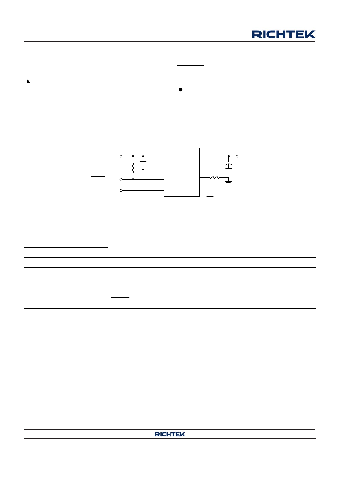
Typical Application Circuit
DNN : Date Code
RT9728CHGQW
3WW
3W : Product Code
W : Date Code
V
FAULT Signal
Chip Enable
IN
R
FAULT
100k
C
IN
10µF
VIN
FAULT
EN
VOUT
RT9728C
Functional Pin Description
Pin No.
SOT-23-6 WDFN-6L 2x2
1 6 VIN Input Voltage.
2
7 (Exposed Pad)
5,
3 4 EN Chip Enable.
4 3
5 2 ILIM
6 1
Pin Name Pin Function
GND
FAULT
Ground. The exposed pad must be soldered to a large PCB and
connected to GND for maximum power dissipation.
Active-Low Open-Drain Output. Asserted during over current, over
temperature, or reverse-voltage conditions.
Current Limit Set Pin. External resistor used to set current limit
threshold. Recommend 19.1k R
VOUT Power Switch Output.
ILIM
GND
V
OUT
150µF
R
ILIM
232k.
ILIM
Copyright 2015 Richtek Technology Corporation. All rights reserved. is a registered trademark of Richtek Technology Corporation.
2
©
DS9728C-00 October 2015www.richtek.com
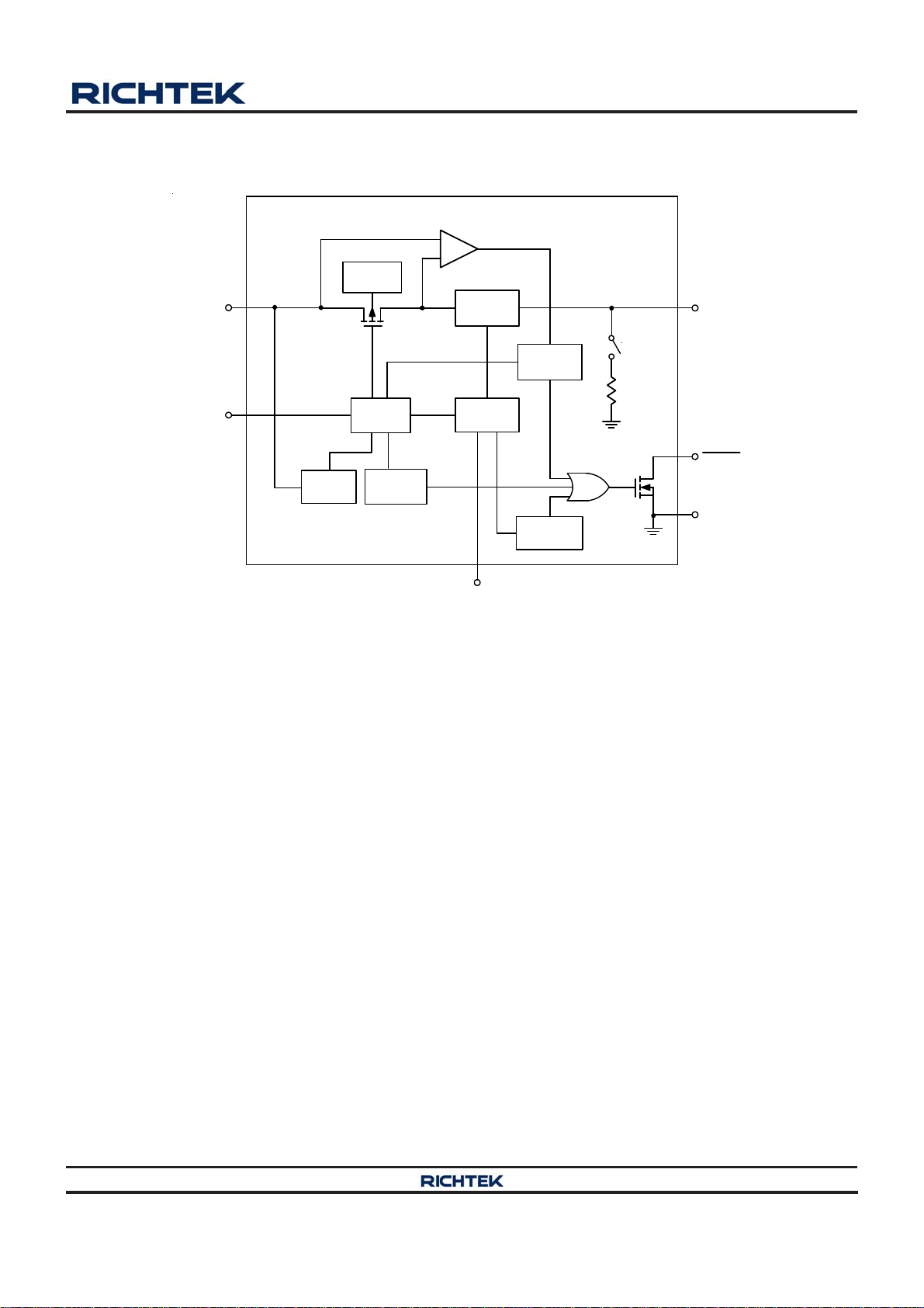
Function Block Diagram
VIN
Switch
well
+
Current
Sense
RT9728C
Reverse Voltage
Comparator
VOUT
EN
UVLO
Drive
Thermal
Sense
Operation
The RT9728C are current-limited, power-distribution
switches using P-channel MOSFETs for applications
where short circuits or heavy capacitive loads will be
encountered. These devices allow the user to program
the current-limit threshold between 75mA and 1.3A (typ)
via an external resistor. Additional device shutdown features
include over temperature protection and reverse-voltage
protection.
Current
Limit
ILIM
4ms
Deglitch
7.5ms
Deglitch
≒60
FAULT
GND
The driver controls the gate voltage of the power switch.
The driver incorporates circuitry that controls the rise and
fall times of the output voltage to limit large current and
voltage surges and provides built-in soft-start functionality.
The RT9728C enters the constant-current mode when the
load exceeds the current-limit threshold.
Copyright 2015 Richtek Technology Corporation. All rights reserved. is a registered trademark of Richtek Technology Corporation.
DS9728C-00 October 2015 www.richtek.com
©
3
RT9728C
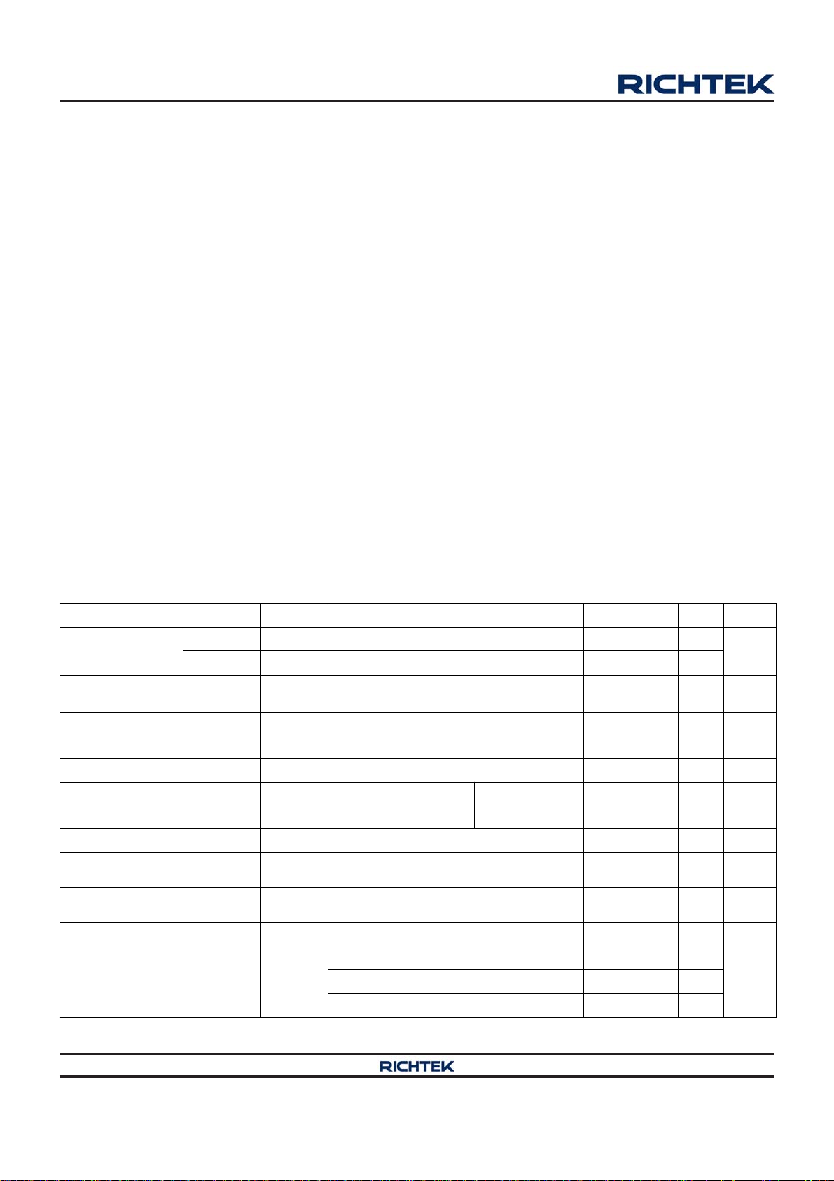
Absolute Maximum Ratings (Note 1)
Supply Input Voltage ------------------------------------------------------------------------------------------------------ −0.3V to 6V
Other Pin Voltage --------------------------------------------------------------------------------------------------------- −0.3V to 6V
Power Dissipation, P
SOT-23-6 -------------------------------------------------------------------------------------------------------------------- 0.4W
WDFN-6L 2x2 -------------------------------------------------------------------------------------------------------------- 0.606W
Package Thermal Resistance (Note 2)
SOT-23-6, θJA--------------------------------------------------------------------------------------------------------------- 250°C/W
WDFN-6L 2x2, θJA--------------------------------------------------------------------------------------------------------- 165°C/W
WDFN-6L 2x2, θJC-------------------------------------------------------------------------------------------------------- 7°C/W
Lead Temperature (Soldering, 10 sec.)------------------------------------------------------------------------------- 260°C
Junction Temperature ----------------------------------------------------------------------------------------------------- 150°C
Storage Temperature Range -------------------------------------------------------------------------------------------- −65°C to 150°C
ESD Susceptibility (Note 3)
HBM (Human Body Model)---------------------------------------------------------------------------------------------- 2kV
Recommended Operating Conditions (Note 4)
@ T
D
= 25°C
A
Supply Input Voltage, VIN ----------------------------------------------------------------------------------------------- 2.5V to 5.5V
Junction Temperature Range -------------------------------------------------------------------------------------------- −40°C to 125°C
Ambient Temperature Range -------------------------------------------------------------------------------------------- −40°C to 85°C
Electrical Characteristics
(VIN = 3.6V, 19.1kΩ ≤ R
Parameter Symbol Test Conditions Min Typ Max Unit
EN Input Voltage
Current Limit Threshold
Resistor Range
Under Voltage Lockout
Threshold
Shutdown Current I
Quiescent Current IQ
Reverse Leakage Current I
Thermal Shutdown
Temperature
Static Drain-Source On-State
Resistance
Current Limit I
≤ 232kΩ, T
ILIM
Logic-High V
= 25°C, unless otherwise specified)
A
1.1 -- --
IH
V
Logic- Low VIL -- -- 0.66
R
(nominal 1%) from I
ILIM
V
Rising -- 2.3 --
V
UVLO
SHDN
V
REV
T
-- 160 -- °C
SD
R
DS(ON)
LIM
IN
VIN Falling -- 2.1 --
VIN = 5.5V, No Load on V
= 5.5V,
V
IN
No Load on V
= 5.5V, VIN = 0V -- 1 3 A
OUT
OUT
ISW = 0.2A -- 120 -- m
= 20k 1190 1295 1400
R
ILIM
R
= 49.9k 468 520 572
ILIM
R
= 210k 110 130 150
ILIM
to GND 19.1 -- 232 k
LIM
, VEN = 0V -- 1 3 A
OUT
R
= 20k -- 120 170
ILIM
R
= 210k -- 120 170
ILIM
V
A
mA
ILIM Shorted to VIN 50 75 100
Copyright 2015 Richtek Technology Corporation. All rights reserved. is a registered trademark of Richtek Technology Corporation.
4
©
DS9728C-00 October 2015www.richtek.com
RT9728C
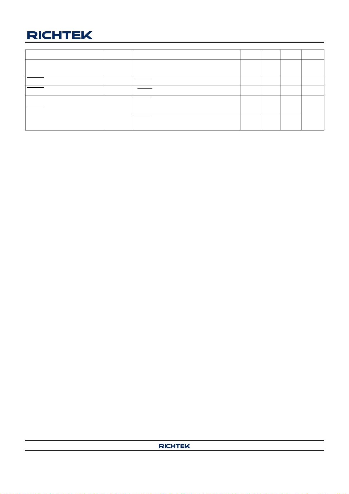
Parameter Symbol Test Conditions Min Typ Max Unit
Reverse Voltage Comparator
Trip Point (V
OUT
VIN)
FAULT Output Low Voltage
FAULT Off State Leakage
FAULT Deglitch
Note 1. Stresses beyond those listed “Absolute Maximum Ratings” may cause permanent damage to the device. These are
stress ratings only, and functional operation of the device at these or any other conditions beyond those indicated in
the operational sections of the specifications is not implied. Exposure to absolute maximum rating conditions may
affect device reliability.
Note 2. θ
Note 3. Devices are ESD sensitive. Handling precaution is recommended.
Note 4. The device is not guaranteed to function outside its operating conditions.
is measured at T
JA
measured at the exposed pad of the package.
-- 135 -- mV
I
= 1mA
V
OL
= 25°C on a low effective thermal conductivity single-layer test board per JEDEC 51-3. θJC is
A
FAULT
V
FAULT
= 5.5V
FAULT assertion or de-assertion due to
over current condition
FAULT assertion or de-assertion due to
reverse voltage condition
-- 180 -- mV
-- 1 -- A
5 7.5 10
ms
2 4 6
Copyright 2015 Richtek Technology Corporation. All rights reserved. is a registered trademark of Richtek Technology Corporation.
DS9728C-00 October 2015 www.richtek.com
©
5

RT9728C
)
)
)
Typical Operating Characteristics
Supply Current vs. Temperature
150
140
130
120
110
100
Supply Current (μA
90
80
-50 -25 0 25 50 75 100 125
Temperature (°C)
On- Resistance vs. Temperature
150
140
130
Ω
120
110
100
90
On-Resistance (m )
80
70
60
-50-25 0 255075100125
VIN = 3.6V
VIN = 5V
Temperature (°C)
Fault Deglitch Timing vs. Temperature
10
9
8
7
6
Fault Deglitch Timing (ms
5
-50 -25 0 25 50 75 100 125
Temperature (°C)
Current Limit vs. Te m perature
1.6
1.5
1.4
1.3
Current Limit (A)
1.2
R
1.1
-50 -25 0 25 50 75 100 125
Temp erature (°C)
ILIM
= 20kΩ
EN Threshold Voltage vs. Temperature
1.5
1.4
1.3
1.2
1.1
1.0
0.9
0.8
0.7
EN Threshold Voltage (V) 1
0.6
0.5
-50 -25 0 25 50 75 100 125
Copyright 2015 Richtek Technology Corporation. All rights reserved. is a registered trademark of Richtek Technology Corporation.
©
Temperature (°C)
Rising
Falling
Under Voltage Lockout vs. Temperature
3.0
2.8
2.6
2.4
2.2
2.0
1.8
1.6
1.4
Under Voltage Lockout (V
1.2
1.0
-50 -25 0 25 50 75 100 125
Temperature (°C)
Rising
Falling
DS9728C-00 October 2015www.richtek.com
6

RT9728C
V
EN
(10V/Div)
V
OUT
(5V/Div)
I
IN
(1A/Div)
V
OUT
(2V/Div)
Fault
(5V/Div)
I
IN
(1A/Div)
Power On from EN
RT9728C, VIN = 5V, C
R
= 20kΩ, R
ILIM
OUT
= 5Ω
Time (500μs/Div)
Current Limit
Full Load (5Ω) to Short Circuit
VIN = 5V, C
R
= 20kΩ
ILIM
OUT
OUT
= 150μF,
= 150μF,
V
EN
(10V/Div)
V
OUT
(5V/Div)
I
IN
(1A/Div)
V
OUT
(2V/Div)
Fault
(5V/Div)
I
IN
(1A/Div)
Power Off from EN
RT9728C, VIN = 5V, C
R
= 20kΩ, R
ILIM
OUT
= 5Ω
Time (500μs/Div)
Current Limit
Short Circuit to Full Load (5Ω)
VIN = 5V, C
R
= 20kΩ
ILIM
= 150μF,
OUT
= 150μF,
OUT
Time (2.5ms/Div)
Current Limit
Short Circuit to No Load
VIN = 5V, C
R
= 20kΩ
ILIM
= 150μF,
OUT
V
OUT
(2V/Div)
Time (2.5ms/Div)
Current Limit
No Load to Short Circuit
VIN = 5V, C
R
= 20kΩ
ILIM
= 150μF,
OUT
V
OUT
(2V/Div)
Fault
Fault
(5V/Div)
(5V/Div)
I
I
IN
(1A/Div)
Time (2.5ms/Div)
Copyright 2015 Richtek Technology Corporation. All rights reserved. is a registered trademark of Richtek Technology Corporation.
©
IN
(1A/Div)
Time (2.5ms/Div)
DS9728C-00 October 2015 www.richtek.com
7

RT9728C
Static Drain-Source Current vs. V
1600
1400
1200
1000
800
600
400
200
Static Drain-Source Current (mA)1
0
0 200 400 600 800 1000
VIN - V
VIN = 5.5V, R
(mV)
OUT
ILIM
- V
IN
= 20kΩ
OUT
Static Drain-Source Current vs. V
160
140
120
100
80
60
40
20
Static Drain-Source Current (mA) 1
0
0 200 400 600 800 1000
VIN - V
VIN = 5.5V, R
(mV)
OUT
ILIM
- V
IN
= 200kΩ
OUT
Copyright 2015 Richtek Technology Corporation. All rights reserved. is a registered trademark of Richtek Technology Corporation.
©
DS9728C-00 October 2015www.richtek.com
8

Applications Information
)
RT9728C
The RT9728C is a single P-MOSFET high-side power
switch with active-high/low enable input, optimized for self-
powered and bus-powered Universal Serial Bus (USB)
applications. The switch's low R
meets USB voltage
DS(ON)
drop requirements and a flag output is available to indicate
fault conditions to the local USB controller.
Current Limiting and Short Circuit Protection
When a heavy load or short circuit situation occurs while
the switch is enabled, large transient current may flow
through the device. The RT9728C includes a current-limit
circuitry to prevent these large currents from damaging
the MOSFET switch and the hub downstream ports. The
RT9728C provides an adjustable current limit threshold
between 120mA and 1.3A (typ) via an external resistor,
R
, between 19.1kΩ and 232kΩ. However, if the ILIM
ILIM
pin is connected to VIN, the current limit threshold will be
75mA (typ). Once the current limit threshold is exceeded,
the device enters constant-current mode until either
thermal shutdown occurs or the fault is removed. The
table1 shows a recommended current limit value vs. R
resistor.
1600
1400
1200
1000
800
600
400
200
Current Limit Threshold (mA
Current Limit Threshold vs. R
0
20 50 80 110 140 170 200 230
R
(k )
Ω
ILIM
Figure 1. Current Limit Threshold vs R
ILIM
ILIM
ILIM
Desired Nominal
Current Limit
(mA)
Table 1. Recommended R
Ide al R esi sto r
(k)
Closet 1%
Resistor (k)
Resistor Selections
ILIM
Actual Limits (Include R Tolerance)
IOS Min (mA) I OS Nom (m A) IOS Max (mA )
75 Short ILI M to VIN 50.0 75.0 100.0
120 226. 1 22 6.0 101. 3 120 .0 142.1
200 134. 0 13 3.0 173. 7 201 .5 233.9
300 88.5 88.7 262. 1 299.4 342.3
400 65.9 66.5 351. 1 396.7 448.7
500 52.5 52.3 443. 9 501.6 562.4
600 43.5 43.2 535. 1 604.6 674.1
700 37.2 37.4 616. 0 696.0 776.0
800 32.4 32.4 708. 7 800.8 892.9
900 28.7 28.7 797. 8 901 .5 1005. 2
1000 25.8 26.1 875. 4 989.1 1102.8
1100 2 3.4 23.2 982. 1 1109.7 1237.3
1200 2 1.4 21.5 1057.9 11 95. 4 13 32. 9
1300 1 9.7 19.6 1178.0 1308.5 1439.0
Copyright 2015 Richtek Technology Corporation. All rights reserved. is a registered trademark of Richtek Technology Corporation.
DS9728C-00 October 2015 www.richtek.com
©
9

RT9728C
Fault Flag
The RT9728C provides a FAULT signal pin which is an N-
channel open drain MOSFET output. This open drain output
goes low when current exceeds current limit threshold,
V
− VIN exceeds reverse voltage trip level, or the die
OUT
temperature exceeds 160°C approximately. The FAULT
output is capable of sinking a 1mA load to typically 180mV
above ground. The FAULT pin requires a pull-up resistor;
this resistor should be large in value to reduce energy
drain. A 100kΩ pull-up resistor works well for most
applications. In case of an over current condition, FAULT
will be asserted only after the flag response delay time,
tD, has elapsed. This ensures that FAULT is asserted upon
valid over current conditions and that erroneous error
reporting is eliminated. For example, false over current
conditions may occur during hot-plug events when
extremely large capacitive loads are connected, which
induces a high transient inrush current that exceeds the
current limit threshold. The FAULT response delay time,
tD, is typically 7.5ms.
Supply Filter/Bypass Ca pa citor
A 10μF low ESR ceramic capacitor connected from VIN to
GND and located close to the device is strongly
recommended to prevent input voltage drooping during hot-
plug events. However, higher capacitor values may be used
to further reduce the voltage droop on the input. Without
this bypass capacitor, an output short may cause sufficient
ringing on the input (from source lead inductance) to
destroy the internal control circuitry. Note that the input
transient voltage must never exceed 6V as stated in the
Absolute Maximum Ratings.
Output Filter Capacitor
A low ESR 150μF aluminum electrolytic capacitor
connected between V
recommended to meet the USB standard maximum droop
requirement for the hub, VBUS. Standard bypass methods
should be used to minimize inductance and resistance
between the bypass capacitor and the downstream
connector to reduce EMI and decouple voltage droop
caused by hot-insertion transients in downstream cables.
Ferrite beads in series with VBUS, the ground line and
the 0.1μF bypass capacitors at the power connector pins
and GND is strongly
OUT
are recommended for EMI and ESD protection. The bypass
capacitor itself should have a low dissipation factor to allow
decoupling at higher frequencies.
Chip Enable Input
The RT9728C will be disabled when the EN pin is in a
logic-low/high condition. During this condition, the internal
circuitry and MOSFET are turned off, reducing the supply
current to 1μA typical. The maximum guaranteed voltage
for a logic-low at the EN pin is 0.66V. A minimum
guaranteed voltage of 1.1V at the EN pin will turn off the
RT9728C. Floating the input may cause unpredictable
operation. EN should not be allowed to go negative with
respect to GND.
Under Voltage Lockout
Under voltage lockout (UVLO) prevents the MOSFET
switch from turning on until input voltage exceeds
approximately 2.3V. If input voltage drops below
approximately 2.1V, UVLO turns off the MOSFET switch
and FAULT will be asserted accordingly. The under voltage
lockout detection functions only when the switch is
enabled.
Thermal Considerations
For continuous operation, do not exceed absolute
maximum junction temperature. The maximum power
dissipation depends on the thermal resistance of the IC
package, PCB layout, rate of surrounding airflow, and
difference between junction and ambient temperature. The
maximum power dissipation can be calculated by the
following formula :
P
where T
the ambient temperature, and θ
D(MAX)
= (T
J(MAX)
− TA) / θ
J(MAX)
JA
is the maximum junction temperature, TA is
is the junction to ambient
JA
thermal resistance.
For recommended operating condition specifications, the
maximum junction temperature is 125°C. The junction to
ambient thermal resistance, θJA, is layout dependent. For
SOT-23-6 packages, the thermal resistance, θJA, is 250°C/
W on a standard JEDEC 51-3 single-layer thermal test
board. For WDFN-6L 2x2 packages, the thermal
resistance, θJA, is 165°C/W on a standard JEDEC 51-3
Copyright 2015 Richtek Technology Corporation. All rights reserved. is a registered trademark of Richtek Technology Corporation.
10
©
DS9728C-00 October 2015www.richtek.com

single-layer thermal test board. The maximum power
dissipation at TA = 25°C can be calculated by the following
formula :
RT9728C
P
= (125°C − 25°C) / (250°C/W) = 0.4W for
D(MAX)
SOT-23-6 package
P
= (125°C − 25°C) / (165°C/W) = 0.606W for
D(MAX)
WDFN-6L 2x2 package
The maximum power dissipation depends on the operating
ambient temperature for fixed T
and thermal
J(MAX)
resistance, θJA. The derating curves in Figure 2 allow the
designer to see the effect of rising ambient temperature
on the maximum power dissipation.
0.65
0.60
0.55
0.50
0.45
0.40
0.35
0.30
0.25
0.20
0.15
0.10
0.05
Maximum Power Dissipation (W) 1
0.00
0 25 50 75 100 125
SOT-23-6
WDFN-6L 2x2
Ambient Temperature (°C)
Single-Layer PCB
Figure 2. Derating Curve of Maximum Power Dissipation
Copyright 2015 Richtek Technology Corporation. All rights reserved. is a registered trademark of Richtek Technology Corporation.
DS9728C-00 October 2015 www.richtek.com
©
11

RT9728C
Outline Dimension
H
D
L
C
b
A
e
Dimensions In Millimeters Dimensions In Inches
Symbol
Min Max Min Max
A 0.889 1.295 0.031 0.051
A1 0.000 0.152 0.000 0.006
B 1.397 1.803 0.055 0.071
b 0.250 0.560 0.010 0.022
C 2.591 2.997 0.102 0.118
B
A1
D 2.692 3.099 0.106 0.122
e 0.838 1.041 0.033 0.041
H 0.080 0.254 0.003 0.010
L 0.300 0.610 0.012 0.024
SOT-23-6 Surface Mount Package
Copyright 2015 Richtek Technology Corporation. All rights reserved. is a registered trademark of Richtek Technology Corporation.
12
©
DS9728C-00 October 2015www.richtek.com

RT9728C
D
E
A
A3
A1
D2
L
E2
SEE DETAIL A
1
e
b
2
1
1
2
DETAIL A
Pin #1 ID and Tie Bar Mark Options
Note : The configuration of the Pin #1 identifier is optional,
but must be located within the zone indicated.
Dimensions In Millimeters Dimensions In Inches
Symbol
Min Max Min Max
A 0.700 0.800 0.028 0.031
A1 0.000 0.050 0.000 0.002
A3 0.175 0.250
b 0.200 0.350 0.008 0.014
D 1.950 2.050 0.077 0.081
D2 1.000 1.450 0.039 0.057
E 1.950 2.050 0.077 0.081
E2 0.500 0.850 0.020 0.033
e 0.650 0.026
L 0.300 0.400
Richtek Technology Corporation
14F, No. 8, Tai Yuen 1st Street, Chupei City
Hsinchu, Taiwan, R.O.C.
Tel: (8863)5526789
0.007 0.010
0.012 0.016
W-Type 6L DFN 2x2 Package
Richtek products are sold by description only. Richtek reserves the right to change the circuitry and/or specifications without notice at any time. Customers should
obtain the latest relevant information and data sheets before placing orders and should verify that such information is current and complete. Richtek cannot
assume responsibility for use of any circuitry other than circuitry entirely embodied in a Richtek product. Information furnished by Richtek is believed to be
accurate and reliable. However, no responsibility is assumed by Richtek or its subsidiaries for its use; nor for any infringements of patents or other rights of third
parties which may result from its use. No license is granted by implication or otherwise under any patent or patent rights of Richtek or its subsidiaries.
DS9728C-00 October 2015 www.richtek.com
13

 Loading...