

RT9715
90m
ΩΩ
Ω, 2A/1.5A/1.1A/0.7A High-Side Power Switches
ΩΩ
with Flag
General Description
The RT9715 is a cost-effective, low-voltage, single
N-MOSFET high-side Power Switch IC for USB application.
Low switch-on resistance (typ. 90mΩ) and low supply
current (typ. 50uA) are realized in this IC.
The RT9715 integrates an over-current protection circuit,
a short fold back circuit, a thermal shutdown circuit and an
under-voltage lockout circuit for overall protection. Besides,
a flag output is available to indicate fault conditions to the
local USB controller. Furthermore, the chip also integrates
an embedded delay function to prevent miss-operation from
happening due to inrush-current. The RT9715 is an ideal
solution for USB power supply and can support flexible
applications since it is available in various packages such
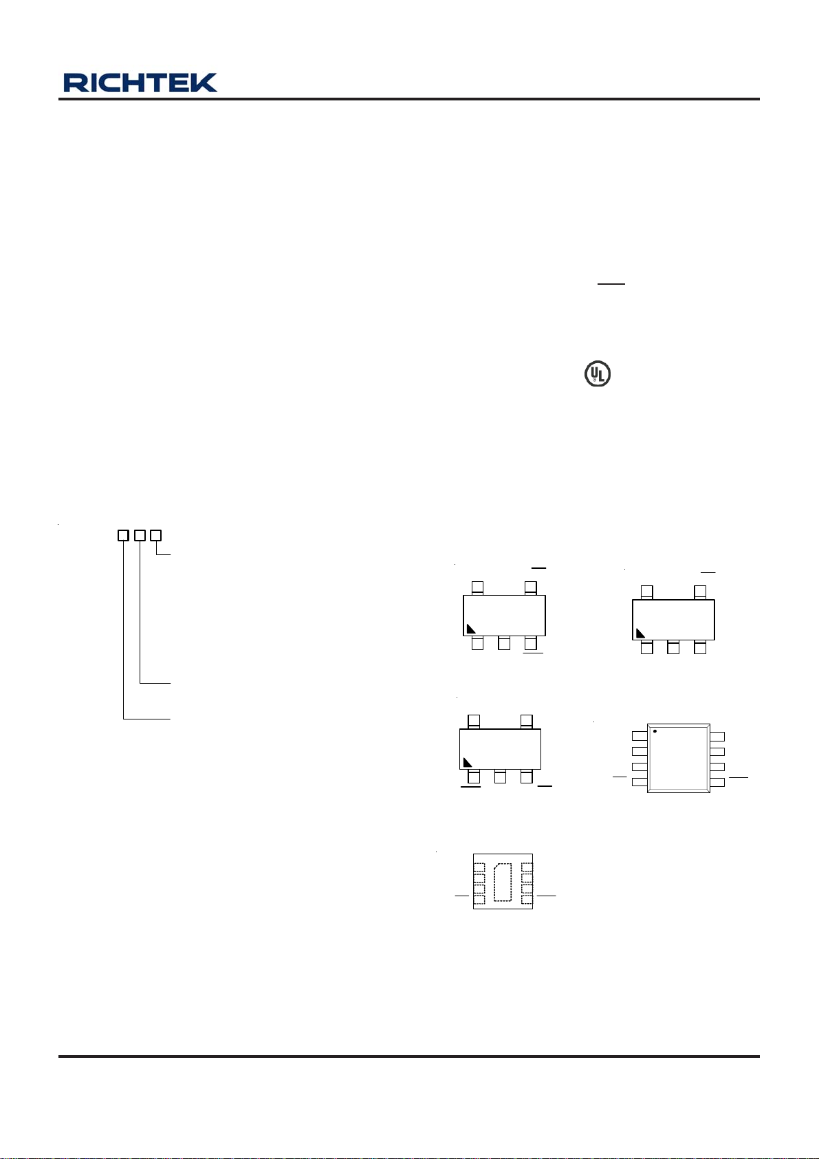
as SOT-23-5, SOP-8, MSOP-8 and WDFN-8L 3x3.
Ordering Information
RT9715
Package Type
B : SOT-23-5
BG : SOT-23-5 (G-Type)
BR : SOT-23-5 (R-Type)
S : SOP-8
F : MSOP-8
QW : WDFN-8L 3x3 (W-Type)
Lead Plating System
G : Green (Halogen Free and Pb Free)
Output Current/EN Function
A : 2A/Active High
B : 2A/Active Low
C : 1.5A/Active High
D : 1.5A/Active Low
E : 1.1A/Active High
F : 1.1A/Active Low
G : 0.7A/Active High
Note :
Richtek products are :
` RoHS compliant and compatible with the current require-
ments of IPC/JEDEC J-STD-020.
` Suitable for use in SnPb or Pb-free soldering processes.
H : 0.7A/Active Low
Features
Ω Ω
zz
90m
Ω (typ.) N-MOSFET Switch
z
zz
Ω Ω
zz
z Operating Range : 2.7V to 5.5V
zz
zz
z Reverse Blocking Current
zz
zz
z Under Voltage Lockout
zz
zz
z Deglitched Fault Report (FLG)
zz
zz
z Thermal Protection with Foldback
zz
zz
z Over Current Protection
zz
zz
z Short Circuit Protection
zz
zz
z UL Approved
zz
zz
z Nemko Approved
zz
zz
z RoHS Compliant and Halogen Free
zz
−−
−E219878
−−
−−
−NO49621
−−
Applications
z USB Peripherals
z Notebook PCs
Pin Configurations
(TOP VIEW)
5
23
SOT-23-5
5
23
GND
1
2
GND
3
9
4
EN/EN
4
FLG
VIN
4
EN/EN
8
7
6
5
VIN
5
VOUT GND
SOT-23-5 (G-Type)
GND
VIN
VIN
EN/EN
SOP-8/MSOP-8
VOUT
VOUT
VOUT
FLG
VIN
VOUT GND
VOUT
FLG
SOT-23-5 (R-Type)
GND
VIN
VIN
EN/EN
WDFN-8L 3x3
Marking Information
EN/EN
23
2
3
4
4
NC
8
7
6
5
VOUT
VOUT
VOUT
FLG
For marking information, contact our sales representative
directly or through a Richtek distributor located in your
area.
DS9715-03 April 2011 www.richtek.com
1

RT9715
Typical Application Circuit
Pull-Up Resistor (10K to 100K)
USB Controller
Supply Voltage
2.7V to 5.5V
RT9715A/C/E/G
Chip Enable
RT9715B/D/F/H
Chip Enable
C
1uF
VIN
IN
EN/EN
Note : A low-ESR 150uF aluminum electrolytic or tantalum between V
the 330mV maximum droop requirement in the hub V
BUS
FLG
RT9715
VOUT
GND
Ferrite
Beads
OUT
. (see Application Information Section for further details)
Functional Pin Description
Pin No .
SOT-23-5
SOT-23-5
(G-Type)
SOT-23-5
(R-Type)
SOP-8 /
MSOP-8
WDFN-8L
3X3
Pin Name Pin Function
1 1 5 6 , 7 , 8 6 , 7 , 8 VOUT Output Voltage.
2 2 2 1 1 GND Ground.
3 -- 1 5 5 FLG Fault FLAG Output.
4 4 3 4 4 EN/EN Chip Enable (Active High/Low).
5 5 4 2 , 3 2 , 3 VIN Power Input Voltage.
-- 3 -- -- -- NC No Internal Connection.
-- -- -- --
9 (Exposed
Pad)
The exposed pad must be soldered to a large
PCB and connected to GND for maximum
power dissipation.
Function Block Diagram
Over -Current
C
OUT
10uF
+
150uF
Data
V
BUS
D+
D-
GND
and GND is strongly recommended to meet
VIN
EN/EN
Bias
Oscillator
UVLO
Charge
Pump
Thermal
Protection
Gate
Control
Current
Limiting
Output Voltage
Detection
Auto Discharge
Delay
VOUT
FLG
GND
DS9715-03 April 2011www.richtek.com
2

Absolute Maximum Ratings (Note 1)
RT9715
z Supply Input Voltage, V
z EN Voltage -------------------------------------------------------------------------------------------------------------- −0.3V to 6V
z FLAG Voltage ---------------------------------------------------------------------------------------------------------- 6V
z Power Dissipation, P
-------------------------------------------------------------------------------------------- 6V
IN
@ TA = 25°C
D
SOT-23-5 ---------------------------------------------------------------------------------------------------------------- 300mW
SOP-8 -------------------------------------------------------------------------------------------------------------------- 469mW
MSOP-8 ----------------------------------------------------------------------------------------------------------------- 469mW
WDFN-8L 3x3 ---------------------------------------------------------------------------------------------------------- 694mW
z Package Thermal Resistance (Note 2)
SOT-23-5, θJA----------------------------------------------------------------------------------------------------------- 250°C/W
SOP-8, θJA-------------------------------------------------------------------------------------------------------------- 160°C/W
MSOP-8, θJA------------------------------------------------------------------------------------------------------------ 160°C/W
WDFN-8L 3x3, θJA----------------------------------------------------------------------------------------------------- 108°C/W
z Junction Temperature ------------------------------------------------------------------------------------------------- 150°C
z Lead Temperature (Soldering, 10 sec.) --------------------------------------------------------------------------- 260°C
z Storage Temperature Range ---------------------------------------------------------------------------------------- −65°C to 150°C
z ESD Susceptibility (Note 3)
HBM (Human Body Mode) ------------------------------------------------------------------------------------------ 2kV
MM (Machine Mode) -------------------------------------------------------------------------------------------------- 200V
Recommended Operating Conditions (Note 4)
z Supply Input Voltage, V
z EN Voltage -------------------------------------------------------------------------------------------------------------- 0V to 5.5V
z Junction Temperature Range ---------------------------------------------------------------------------------------- −40°C to 100°C
z Ambient Temperature Range ---------------------------------------------------------------------------------------- −40°C to 85°C
-------------------------------------------------------------------------------------------- 2.7V to 5.5V
IN
Electrical Characteristics
(VIN = 5V, C
Input Quiescent Current IQ Switch On, V
Input Shutdown Current I
Switch On
Resistance
Current
Limit
Short
Current
= 1uF, C
IN
= 10uF, T
OUT
= 25°C, unless otherwise specified)
A
Parameter Symbol Test Conditions Min Typ Max Unit
= Open -- 50 70
OU T
Switch Off, V
SHDN
RT9715A/B VIN = 5V, I
RT9715C/D VIN = 5V, I
R
RT9715E/F VIN = 5V, I
RT9715G/H
DS(ON)
V
= 5V, I
IN
= Open -- 0.1 1
OUT
= 1.5A -- 90 110
OU T
=1.3A -- 90 110
OU T
= 1A -- 90 110
OU T
= 0.6A -- 90 110
OU T
mΩ
RT9715A/B 2 2.5 3.2
RT9715C/D 1.5 2 2.8
RT9715E/F 1.1 1.5 2.1
RT9715G/H
V
I
LIM
OUT
= 4V
0.7 1 1.4
RT9715A/B -- 1.7 -RT9715C/D -- 1.4 -RT9715E/F -- 1 --
I
SC_FB
RT9715G/H
V
= 0V, Measured Prior to
OUT
Thermal Shutdown
-- 0.7 --
uA
A
A
To be continued
DS9715-03 April 2011 www.richtek.com
3
RT9715
Parameter Symbol Test Conditions Min Typ Max Unit
EN/EN
Thr eshold
EN/EN Input Current I
Output Leakage Current I
Output Turn-On Rise Time T
FLG Output Resistance
FLG Off Current I
Logic_High Voltage VIH V
Logic_Low Voltage V
V
IL
V
EN/EN
LEAKAGE
ON_RISE
R
FLG
FLG_OFF
FLG Delay Time TD
Shutdown Auto-Discharge
Resistance
Under-Voltage Lockout V
Under-Voltage Hysteresis ΔV
R
Discharge
VIN Rising 1.3 1.7 -- V
UVLO
VIN Decreasing -- 0.1 -- V
UVLO
Thermal Shutdown Protection TSD
Thermal Shutdown Hysteresis V
Note 1. Stresses beyond those listed under “Absolute Maximum Ratings” may cause permanent damage to the device.
These are stress ratings only, and functional operation of the device at these or any other conditions beyond those
indicated in the operational sections of the specifications is not implied. Exposure to absolute maximum rating
conditions for extended periods may affect device reliability.
Note 2. θ
Note 3. Devices are ESD sensitive. Handling precaution is recommended.
Note 4. The device is not guaranteed to function outside its operating conditions.
is measured in the natural convection at TA = 25°C on a low effective single layer thermal conductivity test board of
JA
JEDEC 51-3 thermal measurement standard.
= 2.7V to 5.5V 2 -- -- V
IN
= 2.7V to 5.5V -- -- 0.8 V
IN
= 5V
EN
= 0V, R
V
EN
1 0% to 90% of V
I
= 1mA -- 20 -- Ω
SI NK
V
FLG
= 5V
LOAD
= 0Ω
OUT
From fault condition to FLG
assertion
V
= 0V, V
EN
V
> 1V -- 120 -- °C
OUT
V
= 0V -- 100 -- °C
OUT
= 0V -- 20 -- °C
OUT
EN
= 5V
Rising -- 200 -- us
-- 0.01 0.1 uA
-- 0.5 1 uA
-- 0.01 1 uA
5 12 20 ms
-- 100 150 Ω
DS9715-03 April 2011www.richtek.com
4

Typical Operating Characteristics
RT9715
On Resistance vs. Input Voltage
108
I
= 2A
OUT
106
104
102
100
98
96
On Resistance (mΩ)
94
92
90
2.7 3.1 3.5 3.9 4.3 4.7 5.1 5.5
SOP-8
SOT-23-5
Input Voltage (V)
Quiescent Current vs. Input Voltage
60
No Load
58
56
54
52
50
48
46
44
Quiescent Current (uA)
42
40
2.7 3.1 3.5 3.9 4.3 4.7 5.1 5.5
Input Voltage (V)
On Resistance vs. Temperature
125
VIN = 5V, I
120
115
110
105
100
95
90
85
On Resistance (mΩ)
80
75
70
-40 -25 -10 5 20 35 50 65 80
OUT
= 2A
SOP-8
Temperature
SOT-23-5
(°C)
Quiescent Current vs. Temperature
60
VIN = 5V,No Load
59
58
57
56
55
54
53
52
Quiescent Current (uA)
51
50
-40 -25 -10 5 20 35 50 65 80 95 110
Temperature
(°C)
Shutdown Current vs. Input Voltage
1.0
No Load
0.9
0.8
0.7
0.6
0.5
0.4
0.3
0.2
Shutdown Current (uA)
0.1
0.0
2.7 3.1 3.5 3.9 4.3 4.7 5.1 5.5
Input Voltage (V)
Shutdown Current (uA)
Shutdown Current vs. Temperature
1.0
VIN = 5V
0.9
0.8
0.7
0.6
0.5
0.4
0.3
0.2
0.1
0.0
-40 -25 -10 5 20 35 50 65 80 95 110
Temperature
(°C)
DS9715-03 April 2011 www.richtek.com
5

RT9715
Output Voltage vs. Output Current
6.0
5.5
VIN = 5V
5.0
4.5
4.0
VIN = 3.3V
3.5
3.0
2.5
2.0
1.5
Output Voltage (V)
1.0
0.5
0.0
0 0.25 0.5 0.75 1 1.25 1.5 1.75 2 2.25 2.5
Output Current (A)
Current Limit vs. Input Voltage
2.4
2.3
2.2
2.1
UVLO Threshold vs. Temperature
2.2
2.0
1.8
1.6
1.4
Rising
Falling
UVLO Threshold (V)
1.2
1.0
-40 -25 -10 5 20 35 50 65 80 95 110
Temperature
(°C)
Current Limit vs. Temperature
2.40
VIN = 5V
2.35
2.30
2.25
2.0
1.9
Current Limit (A)
1.8
1.7
1.6
2.7 3.1 3.5 3.9 4.3 4.7 5.1 5.5
Input Voltage (V)
Short Current vs . Input Voltage
2.0
1.9
1.8
1.7
1.6
1.5
1.4
1.3
Short Current (A)
1.2
1.1
1.0
2.7 3.1 3.5 3.9 4.3 4.7 5.1 5.5
Input Voltage (V)
2.20
2.15
Current Limit (A)
2.10
2.05
2.00
-40 -25 -10 5 20 35 50 65 80 95 110
Temperature
(°C)
Short Current vs . Te m perature
2.00
VIN = 5V
1.90
1.80
1.70
1.60
1.50
1.40
1.30
Short Current (A)
1.20
1.10
1.00
-40 -25 -10 5 20 35 50 65 80 95 110
Temperature
(°C)
DS9715-03 April 2011www.richtek.com
6

RT9715
FLG Delay Time vs. Input Voltage
12
11
10
9
8
7
6
FLG Delay Time (ms)
5
4
2.7 3.1 3.5 3.9 4.3 4.7 5.1 5.5
Input Voltage (V)
Power On from V
EN = 0V, No Load
IN
FLG Delay Time vs. Temperature
12.0
VIN = 5V
11.5
11.0
10.5
10.0
9.5
9.0
FLG Delay Time (ms)
8.5
8.0
-40 -25 -10 5 20 35 50 65 80 95 110
Temperature
Power Off from V
EN = 0V, No Load
(°C)
IN
V
IN
(2V/Div)
V
OUT
(2V/Div)
V
OUT
(2V/Div)
EN
(5V/Div)
I
IN
(1A/Div)
VIN = 5V, R
Time (25ms/Div)
Power On from EN
= 2.7Ω
LOAD
V
IN
(2V/Div)
V
OUT
(2V/Div)
V
OUT
(2V/Div)
I
IN
(1A/Div)
EN
(5V/Div)
FLG
(5V/Div)
VIN = 5V, R
Time (25ms/Div)
FLG Response
= 0.5Ω
LOAD
Time (100us/Div)
Time (2.5ms/Div)
DS9715-03 April 2011 www.richtek.com
7

RT9715
Applications Information
The RT9715 is a single N-MOSFET high-side power
switches with enable input, optimized for self-powered and
bus-powered Universal Serial Bus (USB) applications. The
RT9715 is equipped with a charge pump circuitry to drive
the internal N-MOSFET switch; the switch's low R
90mΩ, meets USB voltage drop requirements; and a flag
output is available to indicate fault conditions to the local
USB controller.
Input and Output
VIN (input) is the power source connection to the internal
circuitry and the drain of the MOSFET. V
OUT
the source of the MOSFET. In a typical application, current
flows through the switch from VIN to V
If V
is greater than VIN, current will flow from V
OUT
V
since the MOSFET is bidirectional when on.
IN
toward the load.
OUT
Unlike a normal MOSFET, there is no parasitic body diode
between drain and source of the MOSFET, the RT9715
prevents reverse current flow if V
is externally forced to
OUT
a higher voltage than VIN when the chip is disabled (V
0.8V or V
D
Normal MOSFET RT9715
> 2V).
EN
D
S
G
G
Chip Enable Input
The switch will be disabled when the EN/EN pin is in a
logic low/high condition. During this condition, the internal
circuitry and MOSFET will be turned off, reducing the supply
current to 0.1uA typical. Floating the EN/EN may cause
unpredictable operation. EN should not be allowed to go
negative with respect to GND. The EN/EN pin may be
directly tied to V
(GND) to keep the part on.
IN
Soft Start for Hot Plug-In Applications
In order to eliminate the upstream voltage droop caused
by the large inrush current during hot-plug events, the “soft-
start” feature effectively isolates the power source from
extremely large capacitive loads, satisfying the USB voltage
droop requirements.
DS(ON)
(output) is
to
OUT
<
EN
S
Fault Flag
The RT9715 series provides a FLG signal pin which is an
N-Channel open drain MOSFET output. This open drain
output goes low when current limit or the die temperature
exceeds 120°C approximately. The FLG output is capable
,
of sinking a 10mA load to typically 200mV above ground.
The FLG pin requires a pull-up resistor, this resistor should
be large in value to reduce energy drain. A 100kΩ pull-up
resistor works well for most applications. In the case of an
over-current condition, FLG will be asserted only after the
flag response delay time, tD, has elapsed. This ensures
that FLG is asserted only upon valid over-current conditions
and that erroneous error reporting is eliminated.
For example, false over-current conditions may occur
during hot-plug events when extremely large capacitive
loads are connected and causes a high transient inrush
current that exceeds the current limit threshold. The FLG
response delay time t
is typically 12ms.
D
Under-Voltage Lockout
Under-voltage lockout (UVLO) prevents the MOSFET switch
from turning on until input the voltage exceeds
approximately 1.7V. If input voltage drops below
approximately 1.3V, UVLO turns off the MOSFET switch.
Under-voltage detection functions only when the switch is
enabled.
Current Limiting and Short-Circuit Protection
The current limit circuitry prevents damage to the MOSFET
switch and the hub downstream port but can deliver load
current up to the current limit threshold of typically 2A
through the switch of the RT9715A/B, 1.5A for
RT9715C/D, 1.1A for RT9715E/F and 0.7A for
RT9715G/H respectively. When a heavy load or short circuit
is applied to an enabled switch, a large transient current
may flow until the current limit circuitry responds. Once
this current limit threshold is exceeded, the device enters
constant current mode until the thermal shutdown occurs
or the fault is removed.
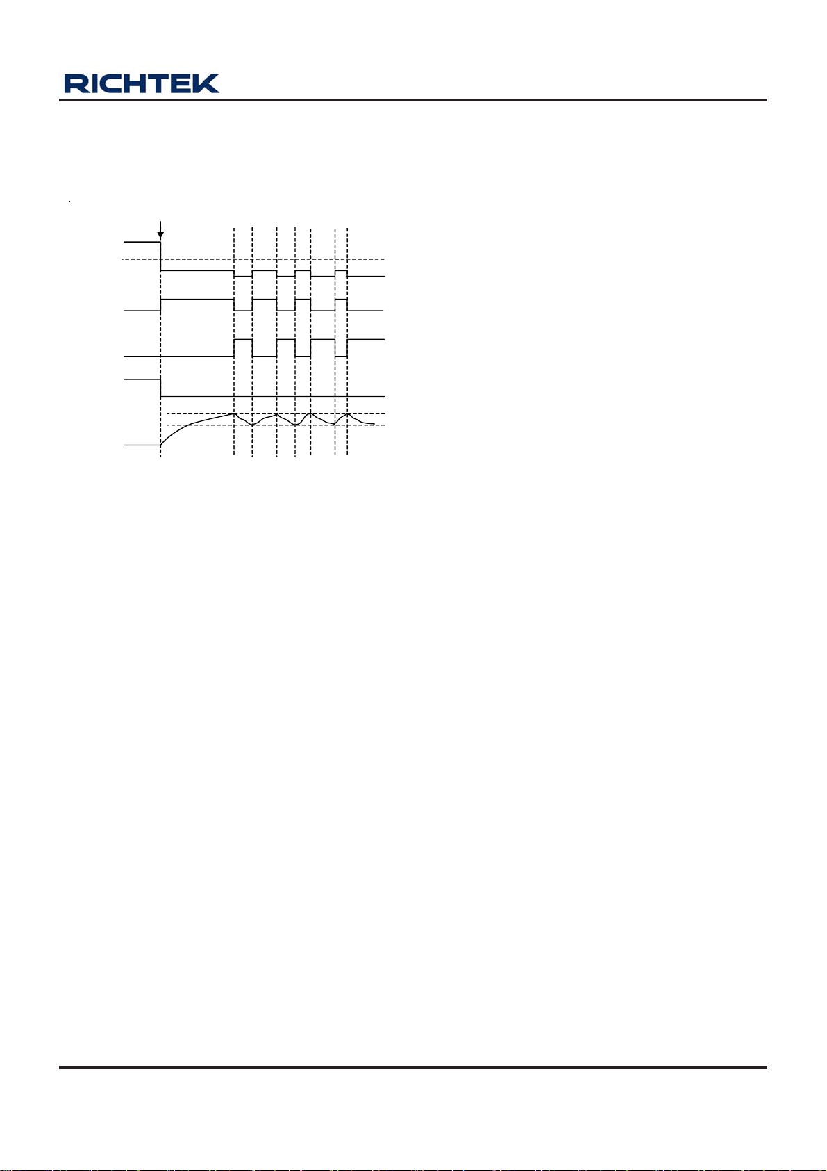
Thermal Shutdown
Thermal protection limits the power dissipation in RT9715.
When the operation junction temperature exceeds 120°C,
the OTP circuit starts the thermal shutdown function and
DS9715-03 April 2011www.richtek.com
8
RT9715
turns the pass element off. The pass element turn on again
after the junction temperature cools to 80°C. The RT9715
lowers its OTP trip level from 120°C to 100°C when output
short circuit occurs (V
V
Short to GND
OUT
V
OUT
I
OUT
Thermal
Shutdown
°
120 C
OTP Trip Point
IC Temperature
100 C
< 1V) as shown in Figure 1.
OUT
°
°
100 C
80 C°
1V
Figure 1. Short Circuit Thermal Folded Back Protection
when Output Short Circuit Occurs (Patent)
Power Dissipation
The junction temperature of the RT9715 series depend on
several factors such as the load, PCB layout, ambient
temperature and package type. The output pin of the
RT9715 can deliver the current of up to 2A (RT9715A/B),
1.5A (RT9715C/D), 1.1A (RT9715E/F) and 0.7A (RT9715G/
H) respectively over the full operating junction temperature
range. However, the maximum output current must be
derated at higher ambient temperature to ensure the
junction temperature does not exceed 100°C. With all
possible conditions, the junction temperature must be within
the range specified under operating conditions. Power
dissipation can be calculated based on the output current
and the R
PD = R
DS(ON)
of the switch as below.
DS(ON)
2
x I
OUT
Although the devices are rated for 2A, 1.5A, 1.1A and 0.7A
of output current, but the application may limit the amount
of output current based on the total power dissipation and
the ambient temperature. The final operating junction
temperature for any set of conditions can be estimated by
the following thermal equation :
P
Where T
D (MAX)
= ( T
J (MAX)
- TA ) / θ
J (MAX)
JA
is the maximum junction temperature of
the die (100°C) and TA is the maximum ambient temperature.
The junction to ambient thermal resistance (θJA) for
SOT-23-5/TSOT-23-5, SOP-8/MSOP-8 and WDFM-8L 3x3
packages at recommended minimum footprint are 250°C/
W, 160°C/W and 108°C/W respectively (θJA is layout
dependent).
Universal Serial Bus (USB) & Power Distribution
The goal of USB is to enable device from different vendors
to interoperate in an open architecture. USB features
include ease of use for the end user, a wide range of
workloads and applications, robustness, synergy with the
PC industry, and low-cost implementation. Benefits include
self-identifying peripherals, dynamically attachable and
reconfigurable peripherals, multiple connections (support
for concurrent operation of many devices), support for as
many as 127 physical devices, and compatibility with PC
Plug-and-Play architecture.
The Universal Serial Bus connects USB devices with a
USB host: each USB system has one USB host. USB
devices are classified either as hubs, which provide
additional attachment points to the USB, or as functions,
which provide capabilities to the system (for example, a
digital joystick). Hub devices are then classified as either
Bus-Power Hubs or Self-Powered Hubs.
A Bus-Powered Hub draws all of the power to any internal
functions and downstream ports from the USB connector
power pins. The hub may draw up to 500mA from the
upstream device. External ports in a Bus-Powered Hub
can supply up to 100mA per port, with a maximum of four
external ports.
Self-Powered Hub power for the internal functions and
downstream ports does not come from the USB, although
the USB interface may draw up to 100mA from its upstream
connect, to allow the interface to function when the
remainder of the hub is powered down. The hub must be
able to supply up to 500mA on all of its external
downstream ports. Please refer to Universal Serial
Specification Revision 2.0 for more details on designing
compliant USB hub and host systems.
Over-Current protection devices such as fuses and PTC
resistors (also called polyfuse or polyswitch) have slow
trip times, high on-resistance, and lack the necessary
circuitry for USB-required fault reporting.
DS9715-03 April 2011 www.richtek.com
9

RT9715
The faster trip time of the RT9715 power distribution allows
designers to design hubs that can operate through faults.
The RT9715 provides low on-resistance and internal fault-
reporting circuitry to meet voltage regulation and fault
notification requirements.
Because the devices are also power switches, the designer
of self-powered hubs has the flexibility to turn off power to
output ports. Unlike a normal MOSFET, the devices have
controlled rise and fall times to provide the needed inrush
current limiting required for the bus-powered hub power
switch.
Supply Filter/Bypass Ca pa citor
A 1uF low-ESR ceramic capacitor from V
to GND, located
IN
at the device is strongly recommended to prevent the input
voltage drooping during hot-plug events. However, higher
capacitor values will further reduce the voltage droop on
the input. Furthermore, without the bypass capacitor, an
output short may cause sufficient ringing on the input (from
source lead inductance) to destroy the internal control
circuitry. The input transient must not exceed 6V of the
absolute maximum supply voltage even for a short duration.
Output Filter Capacitor
A low-ESR 150uF aluminum electrolytic or tantalum
between V
the 330mV maximum droop requirement in the hub V
and GND is strongly recommended to meet
OUT
BUS
(Per USB 2.0, output ports must have a minimum 120uF
of low-ESR bulk capacitance per hub). Standard bypass
methods should be used to minimize inductance and
resistance between the bypass capacitor and the
downstream connector to reduce EMI and decouple voltage
droop caused when downstream cables are hot-insertion
transients. Ferrite beads in series with V
, the ground
BUS
line and the 0.1uF bypass capacitors at the power connector
pins are recommended for EMI and ESD protection. The
bypass capacitor itself should have a low dissipation factor
to allow decoupling at higher frequencies.
Voltage Drop
The USB specification states a minimum port-output voltage
in two locations on the bus, 4.75V out of a Self-Powered
Hub port and 4.40V out of a Bus-Powered Hub port. As
with the Self-Powered Hub, all resistive voltage drops for
the Bus-Powered Hub must be accounted for to guarantee
voltage regulation (see Figure 7-47 of Universal Serial
Specification Revision 2.0 ).
The following calculation determines V
ple ports (N
using one switch per port, N
V
OUT (MIN)
= 4.75V − [ II x ( 4 x R
(0.1A x N
) ganged together through one switch (if
PORTS
is equal to 1) :
PORTS
+ 2 x R
CONN
PORTS
x R
SWITCH
) − V
OUT (MIN)
CABLE
PCB
for multi-
) ] −
Where
R
= Resistance of connector contacts
CONN
(two contacts per connector)
R
= Resistance of upstream cable wires
CABLE
(one 5V and one GND)
R
= Resistance of power switch
SWITCH
(90mΩ typical for RT9715)
V
= PCB voltage drop
PCB
The USB specification defines the maximum resistance
per contact (R
) of the USB connector to be 30mΩ and
CONN
the drop across the PCB and switch to be 100mV. This
basically leaves two variables in the equation: the
resistance of the switch and the resistance of the cable.
If the hub consumes the maximum current (II) of 500mA,
the maximum resistance of the cable is 90mΩ.
The resistance of the switch is defined as follows :
R
= (200mV − V
= { 4.75V − 4.4V − [ 0.5A x ( 4 x 30mΩ + 2 x
SWITCH
90mΩ) ] − V
}÷( 0.1A x N
PCB
)÷( 0.1A x N
PCB
PORTS
PORTS
)
)
If the voltage drop across the PCB is limited to 100mV,
the maximum resistance for the switch is 250mΩ for four
ports ganged together. The RT9715, with its maximum
100mΩ on-resistance over temperature, can fit the demand
of this requirement.
Thermal Considerations
For continuous operation, do not exceed absolute
maximum operation junction temperature. The maximum
power dissipation depends on the thermal resistance of IC
package, PCB layout, the rate of surroundings airflow and
temperature difference between junction to ambient. The
10
DS9715-03 April 2011www.richtek.com

RT9715
maximum power dissipation can be calculated by following
formula :
P
Where T
temperature 100°C, T
θ
= (T
D(MAX)
J(MAX)
is the junction to ambient thermal resistance.
JA
− TA) / θ
J(MAX)
JA
is the maximum operation junction
is the ambient temperature and the
A
For recommended operating conditions specification of
RT9715, where T
is the maximum junction
J(MAX)
temperature of the die (100°C) and TA is the maximum
ambient temperature. The junction to ambient thermal
resistance θJA is layout dependent. For SOT-23-5
packages, the thermal resistance θJA is 250°C/W on the
standard JEDEC 51-3 single-layer thermal test board. And
for SOP-8 and MSOP-8 packages, the thermal resistance
θJA is 160°C/W. The maximum power dissipation at TA =
25°C can be calculated by following formula :
P
= (100°C - 25°C) / (250°C/W) = 0.3W for
D(MAX)
SOT-23-5 packages
P
= (100°C - 25°C) / (160°C/W) = 0.469W for
D(MAX)
SOP-8/MSOP-8 packages
P
= (100°C - 25°C) / (108°C/W) = 0.694W for
D(MAX)
WDFN-8L 3x3 packages
The maximum power dissipation depends on operating
ambient temperature for fixed T
and thermal resistance
J(MAX)
θJA. For RT9715 packages, the Figure 2 of derating curves
allows the designer to see the effect of rising ambient
temperature on the maximum power allowed.
PCB Layout Guide
In order to meet the voltage drop, droop, and EMI
requirements, careful PCB layout is necessary. The
following guidelines must be followed :
` Locate the ceramic bypass capacitors as close as
possible to the VIN pins of the RT9715.
` Place a ground plane under all circuitry to lower both
resistance and inductance and improve DC and transient
performance (Use a separate ground and power plans if
possible).
` Keep all V
least 50-mil, 2 ounce copper for all V
traces as short as possible and use at
BUS
traces.
BUS
` Avoid vias as much as possible. If vias are necessary,
make them as large as feasible.
` Place cuts in the ground plane between ports to help
reduce the coupling of transients between ports.
` Locate the output capacitor and ferrite beads as close to
the USB connectors as possible to lower impedance
(mainly inductance) between the port and the capacitor
and improve transient load performance.
` Locate the RT9715 as close as possible to the output
port to limit switching noise.
The input capacitor should
be placed as close as
possible to the IC.
V
BUS
V
OUT
V
IN
0.8
WDFN-8L 3x3
0.7
0.6
SOP-8/MSOP-8
0.5
0.4
SOT-23-5
0.3
0.2
0.1
Maximum Power Dissipation (W)
0
0 10203040 50607080 90100
Single Layer PCB
GND_BUS
Figure 3
GND
FLG
V
IN
EN
Ambient Temperature (°C)
Figure 2. Derating Curves for RT9715 Package
DS9715-03 April 2011 www.richtek.com
11

RT9715
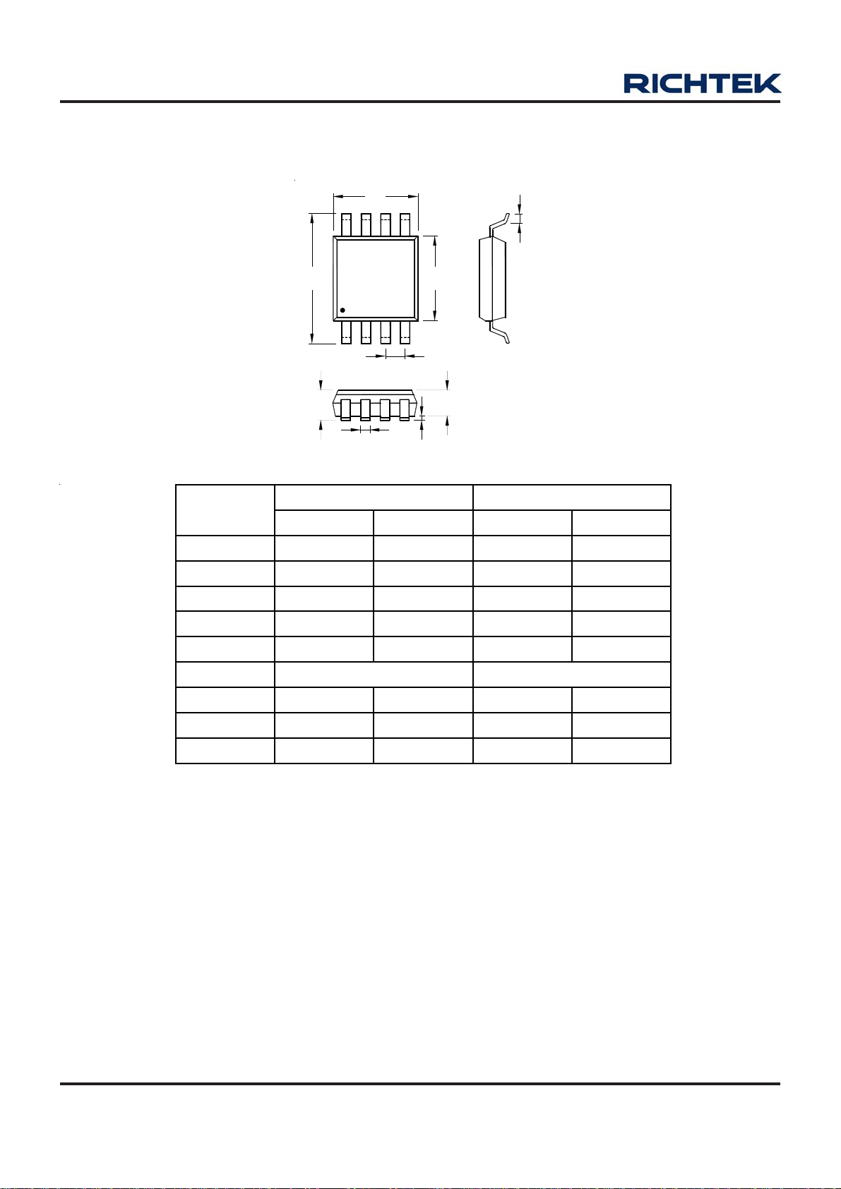
Outline Dimension
H
D
L
C
b
A
e
Dimensions In Millimeters Dimensions In Inches
Symbol
Min Max Min Max
A 0.889 1.295 0.035 0.051
A1 0.000 0.152 0.000 0.006
B 1.397 1.803 0.055 0.071
b 0.356 0.559 0.014 0.022
C 2.591 2.997 0.102 0.118
D 2.692 3.099 0.106 0.122
B
A1
12
e 0.838 1.041 0.033 0.041
H 0.080 0.254 0.003 0.010
L 0.300 0.610 0.012 0.024
SOT-23-5 Surface Mount Package
DS9715-03 April 2011www.richtek.com

RT9715
A
J
I
Dimensions In M illimeters Dimensions In Inches
Symbol
Min Max Min Max
A 4.801 5.004 0.189 0.197
B
F
C
D
H
M
B 3.810 3.988 0.150 0.157
C 1.346 1.753 0.053 0.069
D 0.330 0.508 0.013 0.020
F 1.194 1.346 0.047 0.053
H 0.170 0.254 0.007 0.010
I 0.050 0.254 0.002 0.010
J 5.791 6.200 0.228 0.244
M 0.400 1.270 0.016 0.050
8-Lead SOP Plastic Package
DS9715-03 April 2011 www.richtek.com
13
RT9715
D
L
E
A
b
Dimensions In M illimeters Dimensions In Inches
Symbol
Min Max Min Max
A 0.810 1.100 0.032 0.043
A1 0.000 0.150 0.000 0.006
A2 0.750 0.950 0.030 0.037
b 0.220 0.380 0.009 0.015
D 2.900 3.100 0.114 0.122
e 0.650 0.026
E1
e
A2
A1
14
E 4.800 5.000 0.189 0.197
E1 2.900 3.100 0.114 0.122
L 0.400 0.800
8-Lead MSOP Plastic Package
0.016 0.031
DS9715-03 April 2011www.richtek.com

RT9715
D
E
A
A3
A1
D2
L
E2
SEE DETAIL A
1
e
b
2
1
1
2
DETAIL A
Pin #1 ID and Tie Bar Mark Options
Note : The configuration of the Pin #1 identifier is optional,
but must be located within the zone indicated.
Dimensions In Millimeters Dimensions In Inches
Symbol
Min Max Min Max
A 0.700 0.800 0.028 0.031
A1 0.000 0.050 0.000 0.002
A3 0.175 0.250 0.007 0.010
b 0.200 0.300 0.008 0.012
D 2.950 3.050 0.116 0.120
D2 2.100 2.350 0.083 0.093
E 2.950 3.050 0.116 0.120
E2 1.350 1.600 0.053 0.063
e 0.650 0.026
L 0.425 0.525
Richtek Technology Corporation
Headquarter
5F, No. 20, Taiyuen Street, Chupei City
Hsinchu, Taiwan, R.O.C.
Tel: (8863)5526789 Fax: (8863)5526611
0.017 0.021
W-Type 8L DFN 3x3 Package
Richtek Technology Corporation
Taipei Office (Marketing)
5F, No. 95, Minchiuan Road, Hsintien City
Taipei County, Taiwan, R.O.C.
Tel: (8862)86672399 Fax: (8862)86672377
Email: marketing@richtek.com
Information that is provided by Richtek Technology Corporation is believed to be accurate and reliable. Richtek reserves the right to make any change in circuit design,
specification or other related things if necessary without notice at any time. No third party intellectual property infringement of the applications should be guaranteed
by users when integrating Richtek products into any application. No legal responsibility for any said applications is assumed by Richtek.
DS9715-03 April 2011 www.richtek.com
15

 Loading...