


RT9701
100m
ΩΩ
Ω Power Distribution Switches
ΩΩ
General Description
The RT9701 is an integrated 100mΩ power switch for
self-powered and bus-powered Universal Series Bus
(USB) applications. A built-in charge pump is used to
drive the N-Cha
nnel MOSFET that is free of parasitic
body diode to eliminate any reversed current flow across
the switch when it is powered off. Its low quiescent current
(23uA) and small package (SOT-23-5) is particularly
suitable in battery-powered portable equipment.
Several protection functions include soft start to limit inrush
current during plug-in, current limiting at 1.5A to meet
USB power requirement, and thermal shutdown to protect
damage under over current conditions.
Ordering Information
RT9701
Package Type
B : SOT-23-5
BL : SOT-23-5 (L-Type)
Lead Plating System
P : Pb Free
G : Green (Halogen Free and Pb Free)
Note :
Richtek products are :
` RoHS compliant and compatible with the current require-
ments of IPC/JEDEC J-STD-020.
` Suitable for use in SnPb or Pb-free soldering processes.
Features
zz
z
zz
zz
z Guaranteed 1.1A Continuous Current
zz
zz
z 1.5A Current Limit
zz
zz
z Small SOT-23-5 Package Minimizes Board Space
zz
zz
z Soft Start
zz
zz
z Thermal Protection
zz
zz
z Low 23uA Supply Current
zz
zz
z Wide Input Voltage Range : 2.2V to 6V
zz
zz
z UL Approved - #E219878
zz
zz
z RoHS Compliant and 100% Lead (Pb)-Free
zz
Ω Ω
100m
Ω T yp. High-Side NMOSFET (SOT-23-5)
Ω Ω
Applications
z Battery-Powered Equipment
z Motherboard USB Power Switch
z USB Device Power Switch
z Hot-Plug Power Supplies
z Battery-Charger Circuits
Pin Configurations
(TOP VIEW)
VOUT
5
VOUT
EN
23
GND
VIN
VOUT
4
5
VOUT
VIN
23
VIN
GND
4
SOT-23-5
SOT-23-5 (L-Type)
Marking Information
For marking information, contact our sales representative
directly or through a Richtek distributor located in your
area.
DS9701-16 April 2011 www.richtek.com
Typical Application Circuit
RT9701xBL
V
IN
C
IN
1uF
VIN
VIN
* 470uF, Low ESR Electrolytic
VOUT
VOUT
GND
* C
OUT
470uF
V
OUT
1
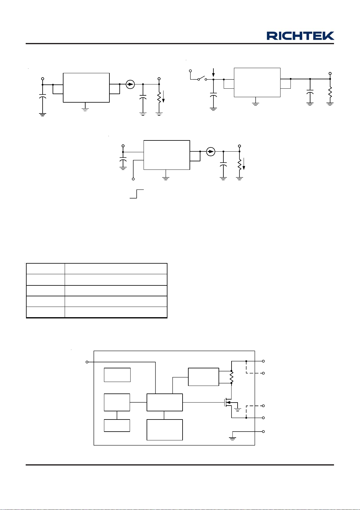
RT9701
Test Circuits
V
IN
VIN
C
1uF
+
IN
VIN
V
C
1uF
IN
IN-SW
+
RT9701xBL
VIN
VIN
GND
RT9701xBL
VOUT
VOUT
GND
I
OUT
V
IN
V
OUT
+
C
L
I
L
R
L
Switch Off
Test Circuit 1 Test Circuit 2
VOUT
VOUT
V
OUT
+
C
L
R
L
V
OUT
+
I
L
L
R
L
C
1uF
IN
V
IN
+
Chip Enable
RT9701xB
VIN
EN
GND
VOUT
VOUT
I
OUT
C
Test Circuit 3
Test Circuit 2 is performed by charging an external tank of bulk capacitor to the input then applying this voltage to the
input of the unit.
All typical operating characteristics curves showed are referred to Test Circuit 1, unless specified to Test Circuit 2 or
Test Circuit 3.
Functional Pin Description
Pin Name Pin Function
VIN Power Input Voltage
VOUT Output Voltage
GND Ground
EN Chip Enable (Active H igh)
Function Block Diagram
EN
Bias
Charge
Pump
Oscillator
2
Control
Thermal
Detection
Current
Limit
NMOSFET
RS
VIN
(VIN)
(VOUT)
VOUT
GND
DS9701-16 April 2011www.richtek.com
RT9701
Absolute Maximum Ratings
z Supply Voltage --------------------------------------------------------------------------------------------------------- 7V
z Chip Enable ------------------------------------------------------------------------------------------------------------- −0.3V to 7V
z Power Dissipation, P
SOT-23-5 ---------------------------------------------------------------------------------------------------------------- 0.25W
z Package Thermal Resistance
SOT-23-5, θJA----------------------------------------------------------------------------------------------------------- 250°C /W
z Lead Temperature (Soldering, 10 sec.) --------------------------------------------------------------------------- 260°C
z Operating Junction Temperature Range -------------------------------------------------------------------------- −20°C to 100°C
z Storage Temperature Range ---------------------------------------------------------------------------------------- −65°C to 150°C
z V
ESD Level
OUT
HBM (Human Body Mode) ------------------------------------------------------------------------------------------ 8kV
MM (Machine Mode) -------------------------------------------------------------------------------------------------- 800V
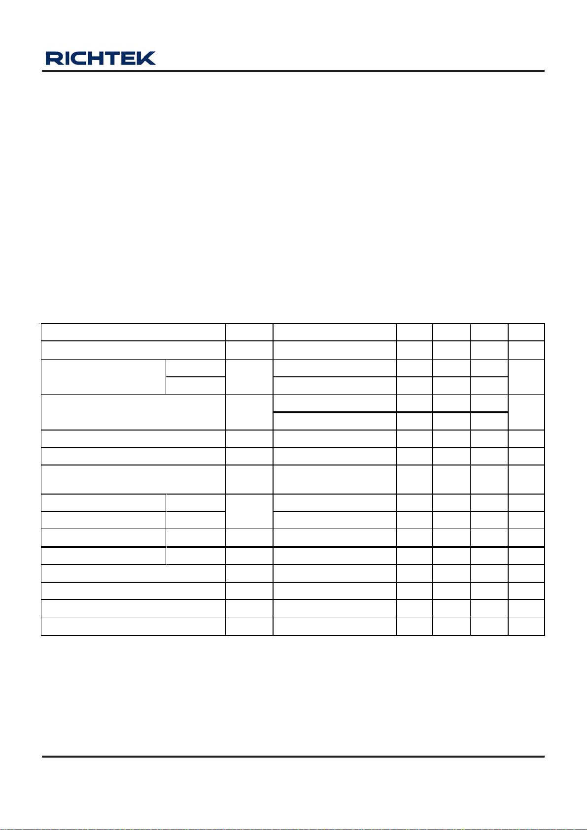
Electrical Characteristics
(V
= 5V, C
IN
= C
IN
OUT
Parameter Symbol Test Conditions Min Typ Max Units
@ T
= 25°C
D
A
= 1μF, TA = 25°C, unless otherwise specified)
Input Voltage Range
RT97 01xBL
Output NMOSFET R
DS(ON)
RT97 01xB
Quiescent Current
Output Turn-On Rising Time
Current Limit Threshold
Short-circuit Fo ld Back Current
EN Input High Threshold RT97 01xB
V
IN
R
DS(ON )
R
T
R
I
LIMIT
I
OS
2.2 -- 6 V
= 1A
I
L
= 1A
I
L
= 3 V
V
IN
VIN = 5 V
= 10Ω, 90% Settling
L
RL = 2Ω
= 0V, measured prior
V
OUT
to thermal shutdown
-- 85 100
mΩ
-- 87 100
-- 19 40
μA
-- 23 45
-- 400 -- μs
1.1 1.5 2 A
-- 1.0 -- A
2.0 -- -- V
EN Input Low Threshold RT97 01xB -- -- 0.8 V
Shutdown S upp ly Current RT97 01xB
Outpu t Lea kage Current RT97 01xB
VIN Under Voltage Lockout
VIN Under Voltage Hysteresis
Thermal Limit
Thermal Limit Hysteresis
I
OFF
I
LEAKAGE
UVLO 1.3 1.8 -- V
-- 100 -- mV
T
SD
ΔT
SD
EN = “0” -- 0.1 1
EN = “0”, V
OUT
= 0V
-- 0.5 10 μ A
-- 130 --
-- 20 --
μA
°C
°C
DS9701-16 April 2011 www.richtek.com
3
RT9701
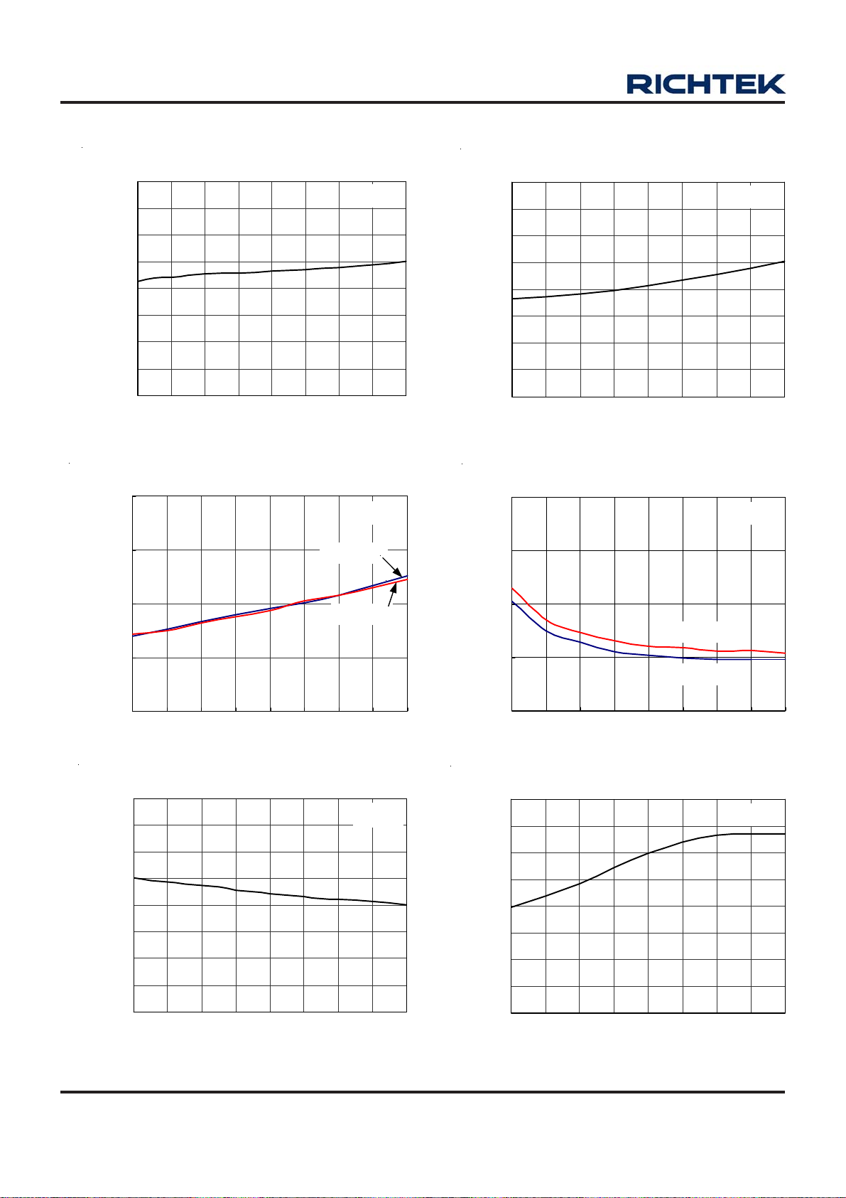
Typical Operating Characteristics
Quiescent Current vs. Temperature
40
35
30
25
20
15
10
Quiescent Current ( uA)
5
0
-40 -20 0 20 40 60 80 100 120
Temperature
(°C)
On-Resistance vs. Temperature
200
150
RT9701xBL
V
V
IN
IN
= 5V
= 5V
Quiescent Current vs. Input Voltage
40
T
35
30
25
20
15
10
Quiescent Current (uA)
5
0
2.0 2.5 3.0 3.5 4.0 4.5 5.0 5.5 6.0
Input Voltage (V)
On -Resistance vs. In put Volt age
100
T
95
= 25°C
A
= 25°C
A
100
50
On-Resistance (mΩ)
0
-40-20 0 20 40 60 80100120
Temperature (℃)
RT9701xB
(°C)
Current Limit vs. Temperature
2.20
2.00
1.80
1.60
1.40
1.20
Current Limit (A)
1.00
0.80
0.60
-40-20 0 20406080100120
Temperature
(°C)
V
IN
= 5V
90
RT9701xB
85
On-Resistance (mΩ)
80
2.0 2.5 3.0 3.5 4.0 4.5 5.0 5.5 6.0
RT9701xBL
Input Voltage(V)
Current Limit vs. Input Voltage
1.80
T
1.58
1.35
1.13
0.90
0.68
Current Limit (A)
0.45
0.23
0.00
2.02.53.03.54.04.55.05.56.0
Input Voltage (V)
A
= 25°C
DS9701-16 April 2011www.richtek.com
4

RT9701
Short Circuit Current vs . Te mp e rature
1400
1300
1200
1100
1000
900
800
700
Short Circuit Current (mA)1
600
500
-40-20 0 204060 80100120
Temperature ( C)
EN Pin Threshold Voltage vs.
EN Threshold vs. Temperature
2.4
2.0
1.6
1.2
0.8
(°C)
EN Threshold (V)
0.4
EN Pin Threshold Voltage (V)
0.0
-40 -20 0 20 40 60 80 100 120
Tempe rature
(°C)
V
V
Rising
Falling
*Test Circuit 3
IN
IN
= 5V
= 5V
Short Circuit Curre nt vs. Input Voltage
1950
T
= 25°C
1700
1450
1200
Short Circuit Current (mA)
EN Threshold (V)
EN Pin Threshold Voltage (V)
A
950
700
450
200
2.0 2.5 3.0 3.5 4.0 4.5 5.0 5.5 6.0
Input Voltage (V)
EN Pin Threshold Voltage vs. Input
EN Threshold vs. Input Voltage
2.4
2.0
1.6
1.2
0.8
0.4
0.0
2.0 2.5 3.0 3.5 4.0 4.5 5.0 5.5 6.0
Input Voltage (V)
T
= 25°C
A
Rising
Falling
*Test Circuit 3
Turn On Rising Time vs. Temperature
720
V
630
540
450
360
270
180
Turn-On Rising Time (us)
90
0
-40-20 0 20406080100120
Temperature
RL =30Ω
C
(°C)
IN
= 1uF Ceramic
L
*Test Circuit 3
= 5V
Turn Off Falling Tim e vs . Temperature
140
120
100
80
60
40
Turn-Off Falling Time (us)
R
= 30Ω
L
20
CL = 1uF Ceramic
0
-40 -20 0 20 40 60 80 100 120
Temperature
(°C)
V
= 5V
IN
*Test Circuit 3
DS9701-16 April 2011 www.richtek.com
5

RT9701
Shutdown Supply Current vs. Temperature
0.9
V
= 5V
IN
0.8
0.6
0.5
0.3
0.2
Shutdown Supply Current (uA)
0.0
-40 -20 0 20 40 60 80 100 120
Temperature
(°C)
*Test Circuit 3
UVLO Threshold vs. Tempe rature
3.50
V
= 5V
IN
3.00
2.50
2.00
Turn-Off Leakage Current vs. Temperature
3.5
V
IN
3.0
2.5
2.0
1.5
1.0
0.5
Turn-Off Leakage Current (uA) A
0.0
-40-200 20406080100120
Temperature
(°C)
*Test Circuit 3
Inrush Current Response
CL = 100uF
CL = 33uF
= 5V
1.50
1.00
UVLO Threshold (V)
0.50
0.00
-40 -20 0 20 40 60 80 100 120
Temperature
(°C)
Turn - On Response
CH1
CH2
CH1: VEN: 5V/Div
L
R
CH2: V
OUT
: 1V/Div
= 30Ω, CL = 1uF
CH1
CH2
CH3
CL = 1uF
IL = 1A/Div, RL = 1Ω, V
Time (100us/Div)
Turn - Off Response
CH1: VEN: 5V/Div
CH2: I
OUT
CH3: V
OUT
RL = 30Ω, CL = 1uF
= 5V
IN
: 100mA/Div
: 2V/Div
Time (100us/Div)
*Test Circuit 3
Time (50us/Div)
*Test Circuit 3
DS9701-16 April 2011www.richtek.com
6

RT9701
CH1
CH2
UVLO at Rising
CH1: VIN: 1V/Div
CH2: V
RL = 30Ω, CL = 1uF
OUT
: 1V/Div
Time (500us/Div)
Inrush Short Circuit Response
CH1: VIN: 2V/Div
V
=1.2V, depend on CIN ESR
DROP
CH1
CH2
CH1: VIN: 1V/Div
CH2: V
RL = 30Ω, CL = 1uF
Soft - start Short Circuit Response
UVLO at Falling
: 1V/ Div
OUT
Time (100ms/Div)
*Test Circuit 2
CH1: VIN: 2V/Div
CH1
CH2
CH1
CH2
CH2: IL: 10A/Div
Ramped Load Response
V
= 5V
OUT
Current Limit Threshold
CH2: I
: 500mA/Div
OUT
I
: depend on ESR & ESL
PEAK
C
= 1uF, CL = 1000uF
IN
Time (25us/Div)
4.9V
V
OUT
1.1V
V
= 5V, CL = 1uF
IN
= 4.6V
CH1
CH2
CH1
CH2
CH2: I
CH2: I
Time (5us/Div)
Current Limit Response
Loading trigger
V
= 5V, C
IN
R
= 1Ω
OUT
: 1A/Div
L
OUT
C
IN
L
: 1A/Div
= 1uF
= 0.1uF
Time (1ms/Div)
Time (5us/Div)
DS9701-16 April 2011 www.richtek.com
7

RT9701
Thermal Shut Dowm Response
CH1
CH3
Thermal Shut Down
CH2
CH1: V
CH2: I
= 5V/Div, CH3: I
EN
@short: 1A/DiV, V
OUT
OUT@RL
= 5V
IN
1Ω: 1A/Div
Time (50ms/Div)
Application Information
The RT9701 is a high-side single N-Channel MOSFET
switch with active-high enable input.
Input and Output
VIN (input) is the power supply connection to the circuitry
and the drain of the output MOSFET. VOUT (output) is
the source of the output MOSFET. In a typical circuit,
current flows through the switch from VIN to VOUT toward
the load. Both VOUT pins must be short on the board
and connected to the load and so do both VIN pins but
connected to the power source.
Current Limiting and Short Protection
The current limit circuit is designed to protect the system
supply, the MOSFET switch and the load from damage
caused by excessive currents. The current limit threshold
is set internally to allow a minimum of 1.1A through the
MOSFET but limits the output current to approximately
1.5A typical. When the output is short to ground, it will
limit to a constant current 1A until thermal shutdown or
short condition removed.
V
IN
C
IN
1uF
CIN = 1uF, C
C
= 1uF, C
IN
= 10uF, C
C
IN
RT9701xBL
VIN
VIN
OUT
OUT
OUT
VOUT
VOUT
GND
= 470uF (Low ESR) on M/B
= 330uF (Low ESR) on Notebook
= 1uF on USB device
V
C
OUT1
OUT
C
V
OUT
OUT2
Figure 1. High Side Power Switch
V
IN
Chip Enable
RT9701xB
C
VIN
IN
EN
GND
VOUT
VOUT
V
C
OUT1
OUT
C
OUT
V
OUT2
Thermal Shutdown
Thermal shutdown shuts off the output MOSFET if the
die temperature exceeds 130°C and 20°C of hysteresis
forces the switch turning off until the die temperature
drops to 110°C.
Soft Start
In order to eliminate the upstream voltage droop caused
by the large inrush current during hot-plug events, the
“soft-start” feature effectively isolates power supplies
from such highly capacitive loads.
Under-voltage Lockout
UVLO prevents the MOSFET switch from turning on until
input voltage exceeds 1.8V (typical). If input voltage drops
below 1.8V (typical), UVLO shuts off the MOSFET switch.
Figure 2. High Side Power Switch
with Chip Enable Control
Filtering
To limit the input voltage drop during hot-plug events,
connect a 1uF ceramic capacitor from VIN to GND.
However, higher capacitor values will further reduce the
voltage drop at the input.
Connect a sufficient capacitor from VOUT to GND. This
capacitor helps to prevent inductive parasitics from pulling
VOUT negative during turn-off or EMI damage to other
components during the hot-detachment. It is also
necessary for meeting the USB specification during hot
plug-in operation. If RT9701 is implanted in device end
application, minimum 1uF capacitor from VOUT to GND is
recommended and higher capacitor values are also
preferred.
DS9701-16 April 2011www.richtek.com
8

In choosing these capacitors, special attention must be
paid to the Effective Series Resistance, ESR, of the
capacitors to minimize the IR drop across the capacitor
ESR. A lower ESR on this capacitor can get a lower IR
drop during the operation.
Ferrite beads in series with all power and ground lines are
recommended to eliminate or significantly reduce EMI. In
selecting a ferrite bead, the DC resistance of the wire
used must be kept to a minimum to reduce the voltage
drop.
Reverse current preventing
The output MOSFET and driver circuitry are also designed
to allow the MOSFET source to be externally forced to a
higher voltage than the drain (VOUT > VIN ≥0). To prevent
reverse current from such condition, disable the switch
(RT9701xB) or connect VIN to a fixed voltage under 1.3V.
RT9701
Layout and Thermal Dissipation
z Place the switch as close to the USB connector as
possible. Keep all traces as short as possible to reduce
the effect of undesirable parasitic inductance.
z Place the ot capacitor and ferrite beads asclose to the
USB connector as possible.
z If ferrite beads are used, use wires with minimum
resistance and large solder pads to minimize
connection resistance.
z If the package is with dual VOUT or VIN pins, short
both the same function pins as Figure 1 or Figure 2 to
reduce the internal turn-on resistance. If the output
power will be delivered to two individual ports, it is
specially necessary to short both VOUT pin at the
switch output side in order to protect the switch when
each port are plug-in separately.
z Under normal operating conditions, the package can
dissipate the channel heat away. Wide power-bus
planes connected to VIN and VOUT and a ground plane
in contact with the device will help dissipate additional
heat.
DS9701-16 April 2011 www.richtek.com
9

RT9701
Outline Dimension
H
D
L
C
b
A
e
B
A1
Dimensions In Millimeters Dimensions In Inches
Symbol
Min Max Min Max
A 0.889 1.295 0.035 0.051
A1 0.000 0.152 0.000 0.006
B 1.397 1.803 0.055 0.071
b 0.356 0.559 0.014 0.022
C 2.591 2.997 0.102 0.118
D 2.692 3.099 0.106 0.122
e 0.838 1.041 0.033 0.041
H 0.080 0.254 0.003 0.010
L 0.300 0.610 0.012 0.024
SOT-23-5 Surface Mount Package
Richtek Technology Corporation
Headquarter
5F, No. 20, Taiyuen Street, Chupei City
Hsinchu, Taiwan, R.O.C.
Tel: (8863)5526789 Fax: (8863)5526611
Information that is provided by Richtek Technology Corporation is believed to be accurate and reliable. Richtek reserves the right to make any change in circuit
design, specification or other related things if necessary without notice at any time. No third party intellectual property infringement of the applications should be
guaranteed by users when integrating Richtek products into any application. No legal responsibility for any said applications is assumed by Richtek.
10
Richtek Technology Corporation
Taipei Office (Marketing)
5F, No. 95, Minchiuan Road, Hsintien City
Taipei County, Taiwan, R.O.C.
Tel: (8862)86672399 Fax: (8862)86672377
Email: marketing@richtek.com
DS9701-16 April 2011www.richtek.com

 Loading...