

查询RT9261B供应商
Preliminary
General Description
The RT9401A/B are digital to analog converters which
generate a reference
voltage for Intel VR10.x/AMD K8
5-bit VID code respectively. The parts are proposed to
pair with a series of RichTek’s general purpose PWM
controllers dedicated for the desktop microprocessor core
power voltage regulation. The reference voltage is within
1% high accuracy. These parts use a small footprint
package of SOT-23-8.
Ordering Information
RT9401A/B
Package Type
V8 : SOT-23-8
Operating Temperature Range
C : Commercial Standard
P : Pb Free with Commercial Standard
K8
VR10.X
Note :
RichTek Pb-free products are :
−RoHS compliant and compatible with the current require ments of IPC/JEDEC J-STD-020.
−Suitable for use in SnPb or Pb-free soldering processes.
−100%matte tin (Sn) plating.
RT9401A/B
5Bit VID Reference Generator
Features
zz
RT9401A Support 5bit DAC Voltage Conforming to
z
zz
Intel VRD10.x VID Table
zz
z RT9401B Support 5bit DAC Voltage Conforming to
zz
AMD K8 VID Table
zz
z 1% High Accuracy of V
zz
zz
z Small Footprint Package of SOT-23-8
zz
zz
z RoHS Compliant and 100% Lead (Pb)-Free
zz
Applications
z Desktop/Motherboard Microprocessor Core Power
Regulation
z High Accuracy and Programmable Voltage Power
Regulation
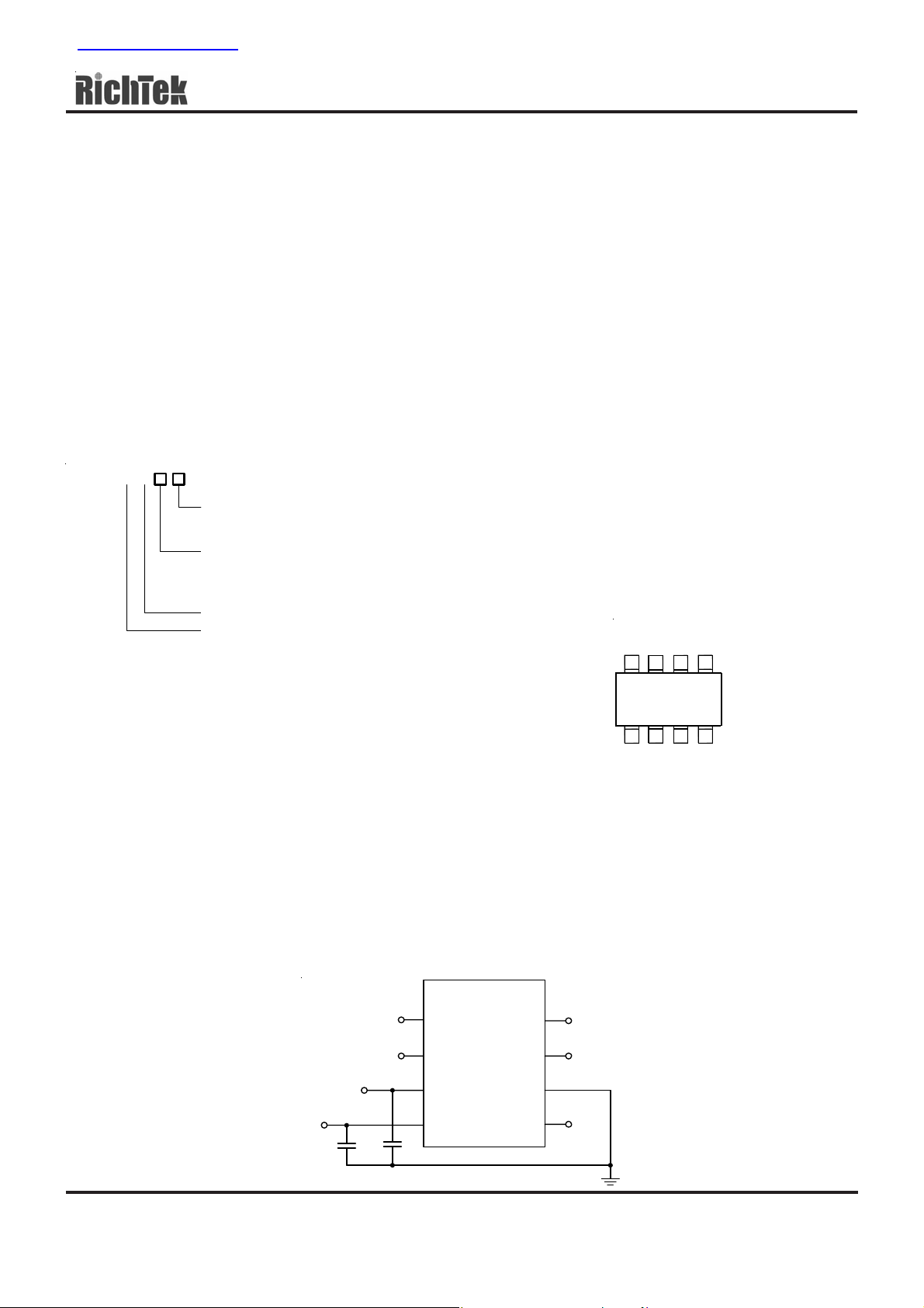
Pin Configurations
REF
(TOP VIEW)
VID3
1
VID2
SOT-23-8
VID4
7
2
VID1
GND
68
34
VDA
VID0
5
VDD
Marking Information
For marking information, contact our sales re presentative
directly or through a RichTek distributor located in your
Note : There is no pin1 indicator on top mark for SOT-23-8
type, and pin 1 will be lower left pin when reading top mark
from left to right.
area, otherwise visit our website for detail.
Typical Application Circuit
RT9401A/B
1
VID2
2
VID1
3
VDA
CL
4
VDD
5V
DS9401A/B-04 June 2005 www.richtek.com
VID3
VID4
GND
VID0
8
7
6
5
1
RT9401A/B
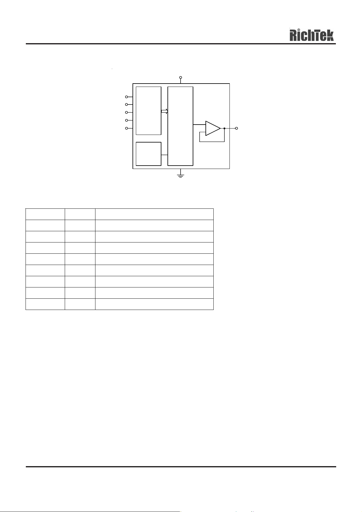
Function Block Diagram
VID4
VID3
VID2
VID1
VID0
Functional Pin Description
Preliminary
VID
Input
V
REF
VDD
MUX
+
-
VDA
Pin Number Pin Name Pin Function
1 VID2 DAC Voltage Identification Inputs
2 VID1 DAC Voltage Identification Inputs
3 VDA Digital - to - Analog Voltage Output
4 VDD Power Input Pin
5 VID0 DAC Voltage Identification Inputs
6 GND Ground
7 VID4 DAC Voltage Identification Inputs
8 VID3 DAC Voltage Identification Inputs
DS9401A/B-04 June 2005www.richtek.com
2
Preliminary
Absolute Maximum Ratings (Note 1)
RT9401A/B
z Supply Input V oltage, V
z Power Dissipation, P
------------------------------------------------------------------------------------------- 7V
DD
@ TA = 25°C
D
SOT-23-8 ---------------------------------------------------------------------------------------------------------------- 0.4W
z Package Thermal Resistance (Note 4)
SOT-23-8, θJA----------------------------------------------------------------------------------------------------------- 250°C/W
z Lead Temperature (Soldering, 10 sec.)--------------------------------------------------------------------------- 260°C
z Storage T emperature Range ---------------------------------------------------------------------------------------- −65°C to 150°C
z ESD Susceptibility (Note 2)
HBM (Human Body Mode) ------------------------------------------------------------------------------------------ 2kV
MM (Ma chine Mode)-------------------------------------------------------------------------------------------------- 200V
Recommended Operating Conditions (Note 3)
z Supply Input V oltage, V
z Junction T emperature Range---------------------------------------------------------------------------------------- −40°C to 125°C
------------------------------------------------------------------------------------------- 5V ±10%
DD
Electrical Characteristics
(V
= 5V, T
DD
VDD Supply Current
= 25° C, unless otherwise specified)
A
Parameter Symbol Test Conditions Min Typ Max Units
Nominal Supply Current IDD VDA open -- 2 5 mA
Reference & DAC
Output Voltage Program See Table 1 & Table 2
VDA ≥ 1V -1 -- +1 %
DAC Output Voltage Accuracy
VDA < 1V -10 -- +10 mV
VID(4:0) Input Low -- 0.65 -- V
VID(4:0) Input High 1.05 -- -- V
VID[4:0] Internal Pull-High Current
Source Capability
When select AMD CPU 2.2 2.4 2.5 V
18 -- -- μA
VID[4:0] Internal Pull-H igh Vol tag e
When select Intel CPU 1 1.1 1.2 V
Output Buffer
DC Gain Capacitor Load Only -- 70 -- dB
Bandwidth GBW CL=1nF -- 1.64 -- MHz
Slew Rate SR CL=0.1uF -- 9.5 -- mV/μs
Impedance R
60 -- 110 Ω
OUT
DS9401A/B-04 June 2005 www.richtek.com
3

RT9401A/B
Note 1. Stresses listed as the above "Absolute Maximum Ratings" may cause permanent damage to the device. These are for
stress ratings. Functional operation of the device at these or any other conditions beyond those indicated in the operational
sections of the specifications is not implied. Exposure to absolute maximum rating conditions for extended periods may
remain possibility to affect device reliability.
Note 2. Devices are ESD sensitive. Handling precaution recommended.
Note 3. The device is not guaranteed to function outside its operating conditions.
Note 4. θJA is measured in the natural convection at TA = 25°C on a low effective thermal conductivity test board of
JEDEC 51-3 thermal measurement standard.
Preliminary
DS9401A/B-04 June 2005www.richtek.com
4

Preliminary
Table 1. Output Voltage Program (VR 10)
RT9401A/B
Pin Name
VID4 VID3 VID2 VID1 VID0
1 1 1 1 1 OFF
0 1 0 0 1 0.850V
0 1 0 0 0 0.875V
0 0 1 1 1 0.900V
0 0 1 1 0 0.925V
0 0 1 0 1 0.950V
0 0 1 0 0 0.975V
0 0 0 1 1 1.000V
0 0 0 1 0 1.025V
0 0 0 0 1 1.050V
0 0 0 0 0 1.075V
1 1 1 1 0 1.100V
1 1 1 0 1 1.125V
1 1 1 0 0 1.150V
1 1 0 1 1 1.175V
Nominal Output Voltage VDA
1 1 0 1 0 1.200V
1 1 0 0 1 1.225V
1 1 0 0 0 1.250V
1 0 1 1 1 1.275V
1 0 1 1 0 1.300V
1 0 1 0 1 1.325V
1 0 1 0 0 1.350V
1 0 0 1 1 1.375V
1 0 0 1 0 1.400V
1 0 0 0 1 1.425V
1 0 0 0 0 1.450V
0 1 1 1 1 1.475V
0 1 1 1 0 1.500V
0 1 1 0 1 1.525V
0 1 1 0 0 1.550V
0 1 0 1 1 1.575V
0 1 0 1 0 1.600V
Note: (1) 0 : Connected to GND
(2) 1 : Open
DS9401A/B-04 June 2005 www.richtek.com
5

RT9401A/B
VID4 VID3 VID2 VID1 VID0 Nominal Output Voltage VDA
0 0 0 0 0 1.550
0 0 0 0 1 1.525
0 0 0 1 0 1.500
0 0 0 1 1 1.475
0 0 1 0 0 1.450
0 0 1 0 1 1.425
0 0 1 1 0 1.400
0 0 1 1 1 1.375
0 1 0 0 0 1.350
0 1 0 0 1 1.325
0 1 0 1 0 1.200
0 1 0 1 1 1.275
0 1 1 0 0 1.250
Preliminary
Table 2. Output Voltage Program (K8)
0 1 1 0 1 1.225
0 1 1 1 0 1.200
0 1 1 1 1 1.175
1 0 0 0 0 1.150
1 0 0 0 1 1.125
1 0 0 1 0 1.100
1 0 0 1 1 1.075
1 0 1 0 0 1.050
1 0 1 0 1 1.025
1 0 1 1 0 1.000
1 0 1 1 1 0.975
1 1 0 0 0 0.950
1 1 0 0 1 0.925
1 1 0 1 0 0.900
1 1 0 1 1 0.875
1 1 1 0 0 0.850
1 1 1 0 1 0.825
1 1 1 1 0 0.800
1 1 1 1 1 Shutdown
Note: (1) 0 : Connected to GND
(2) 1 : Open
DS9401A/B-04 June 2005www.richtek.com
6

Preliminary
Typical Operating Characteristics
RT9401A/B
V
vs. Tempe rature
1.21
1.205
1.2
1.195
VDA
(V)
1.19
VDA
V
1.185
1.18
1.175
-40 -20 0 20 40 60 80 100 120 140
Temperature
(°C)
VID on the Fly Falling
V
= 1.3V to 1.0625V
VDA
No Load
Error Between V
0.7
0.6
0.5
0.4
(%)
VDA
0.3
VID
& V
VDA
- V
0.2
VID
V
0.1
0
0.85 0.975 1.1 1.225 1.35 1.475 1.6
V
(V)
VID
VID on the Fly Rising
V
= 1.3V to 1.0625V
VDA
No Load
VDA (100mV/Div)
Time (25μs/Div)
VDA (100mV/Div)
VID0 (1V/Div)
VID0 (1V/Div)
Time (25μs/Div)
DS9401A/B-04 June 2005 www.richtek.com
7

RT9401A/B
Outline Dimension
Preliminary
H
D
L
C
b
A
e
Dimensions In Millimeters Dimensions In Inches
Symbol
Min Max Min Max
A 1.000 1.450 0.039 0.057
A1 0.000 0.150 0.000 0.006
B 1.500 1.700 0.059 0.067
b 0.220 0.500 0.009 0.020
C 2.600 3.000 0.102 0.118
D 2.800 3.000 0.110 0.118
e 0.585 0.715 0.023 0.028
B
A1
H 0.100 0.220 0.004 0.009
L 0.300 0.600 0.012 0.024
RICHTEK TECHNOLOGY CORP .
Headquarter
5F, No. 20, Taiyuen Street, Chupei City
Hsinchu, Taiwan, R.O.C.
Tel: (8863)5526789 Fax: (8863)5526611
8
SOT-23-8 Surface Mount Package
RICHTEK TECHNOLOGY CORP .
Taipei Office (Marketing)
8F-1, No. 137, Lane 235, Paochiao Road, Hsintien City
Taipei County, Taiwan, R.O.C.
Tel: (8862)89191466 Fax: (8862)89191465
Email: marketing@richtek.com
DS9401A/B-04 June 2005www.richtek.com
 Loading...