RT9230
1.5V Advanced Dual PWM and Dual Linear Power Controller
General Description
The RT9230 is a 4-in-one power controller optimized
for high-performance microprocessor and computer
applications. The IC integrates two PWM controller,
two linear controllers as well as monitoring and
protection functions into a 28-pin SOP package. The
first PWM controller regulates the microprocessor
core voltage with a synchronous buck converter,
while the second PWM controller supplies the
computer system’s AGP 1.5V or 3.3V bus power with
a standard buck converter. The first linear regulator
provides power for the 1.5V GTL bus and the second
linear regulator provides 1.8V power for the
North/South Bridge core voltage and/or cache
memory circuits.
The RT9230 features an Intel-compatible, TTL 5-bit
programmable DAC that adjusts the core voltage
from 2.1V to 3.5V in 0.1V increments and from 1.3V
to 2.05V in 0.05V steps. The 5-bit DAC has a typical
±1% tolerance. The second PWM controller is user-
selectable for output level of 1.5V and 3.3V with
±2.5% accuracy. The linear controllers drives
external N-MOSFET or NPN bipolar for the pass
transistor to provide fixed output voltages of 1.5V
±3% and 1.8V ±3%.
The RT9230 monitors all the output voltages. A
Power -good signal is issued when the core voltage
is within ±10% of the DAC setting and the other
levels are above their under-voltage levels.
Additional build-in over-voltage protection for the
core output uses the lower MOSFET to prevent
output voltage above 115% of the DAC setting. The
PWM over-current function monitors the output
current using the voltage drop across the MOSFET’s
R
, which eliminates the need for a current
DS(ON)
sensing resistor.
Ordering Information
RT9230
Package type
S : SOP-28
Operating temperature range
C: Commercial standard
Features
z
4-in-one Regulated Voltages for Microprocessor
Core, AGP Bus, North/South Bridge and/or
Cache Memory, GTL Bus Power
z
Compatible with HIP6020
z
Power-good Output Voltage Monitor
Switching section
z
5-bit DAC Programmable from 1.3V to 3.5V
z ±
±1% DAC Accuracy
±±
z
Fast Transient Response
z
Full 0% to 100% Duty Cycle Driver
z
Fixed 200kHz Switching Frequency
z
Adaptive Non-overlapping Gate Driver
z
Over-current Monitor Uses MOSFET R
z
Over-voltage Protection Uses Lower MOSFET
DS(ON)
Linear Section
z
Fixed Linear Regulator Output Voltage
z
MOSFET or NPN Driving Capability
z
Ultra Fast Response Speed
z
Under-voltage Protection
z
Internal Thermal Shutdown
Applications
Full Motherboard Power Regulation for Computer
z
Low-voltage Distributed Power Supplies
z
Pin Configurations
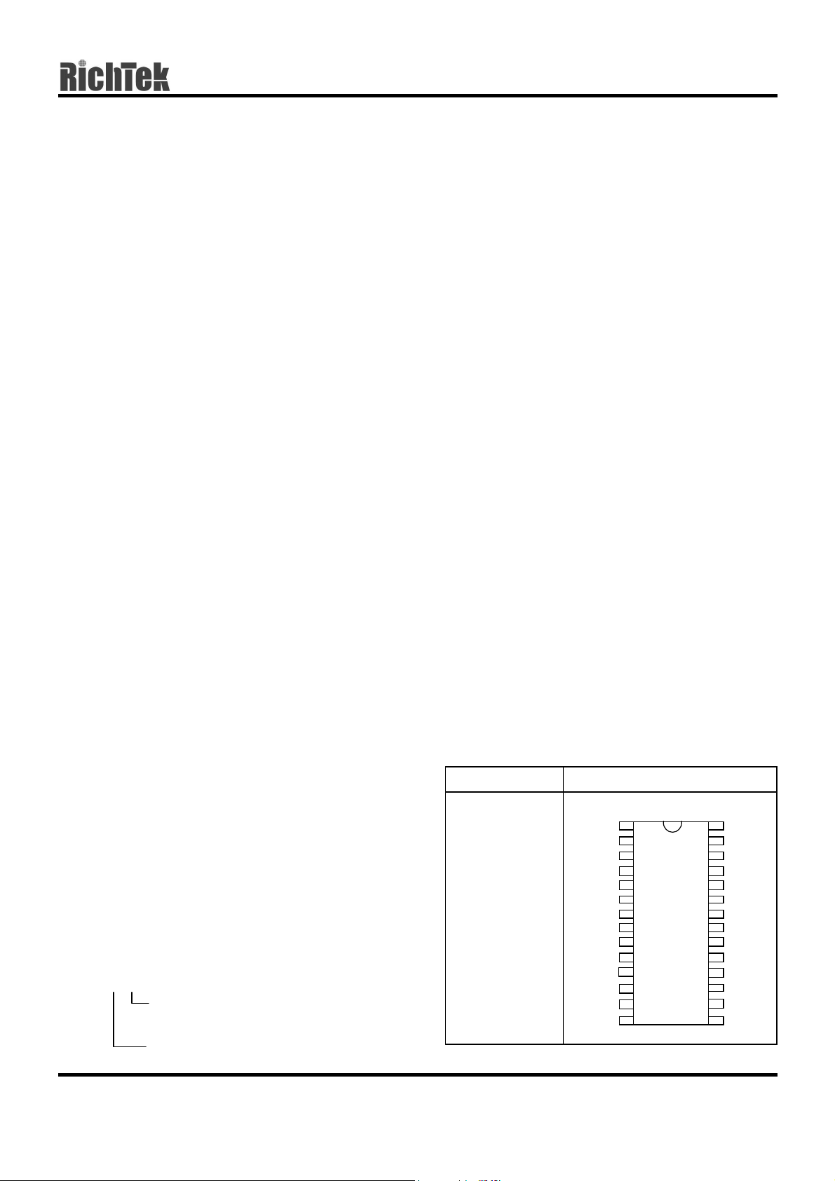
Part Number Pin Configurations
RT9230CS
(Plastic SOP-28)
UGATE2
PHASE2
VID4
VID3
VID2
VID1
VID0
PGOOD
OCSET2
VSEN2
SELECT
FAULT
VSEN4
TOP VIEW
1
2
3
4
5
6
7
8
9
10
11
12 17
SS
13
14
28
27
26
25
24
23
22
21
20
19
18
16
15
VCC
UGATE1
PHASE1
LGATE1
PGND
OCSET1
VSEN1
FB1
NC
VSEN3
DRIVE3
GND
VAUX
DRIVE4
DS9230-03 July 2001 www.richtek-ic.com.tw
1

RT9230
Absolute Maximum Ratings
z
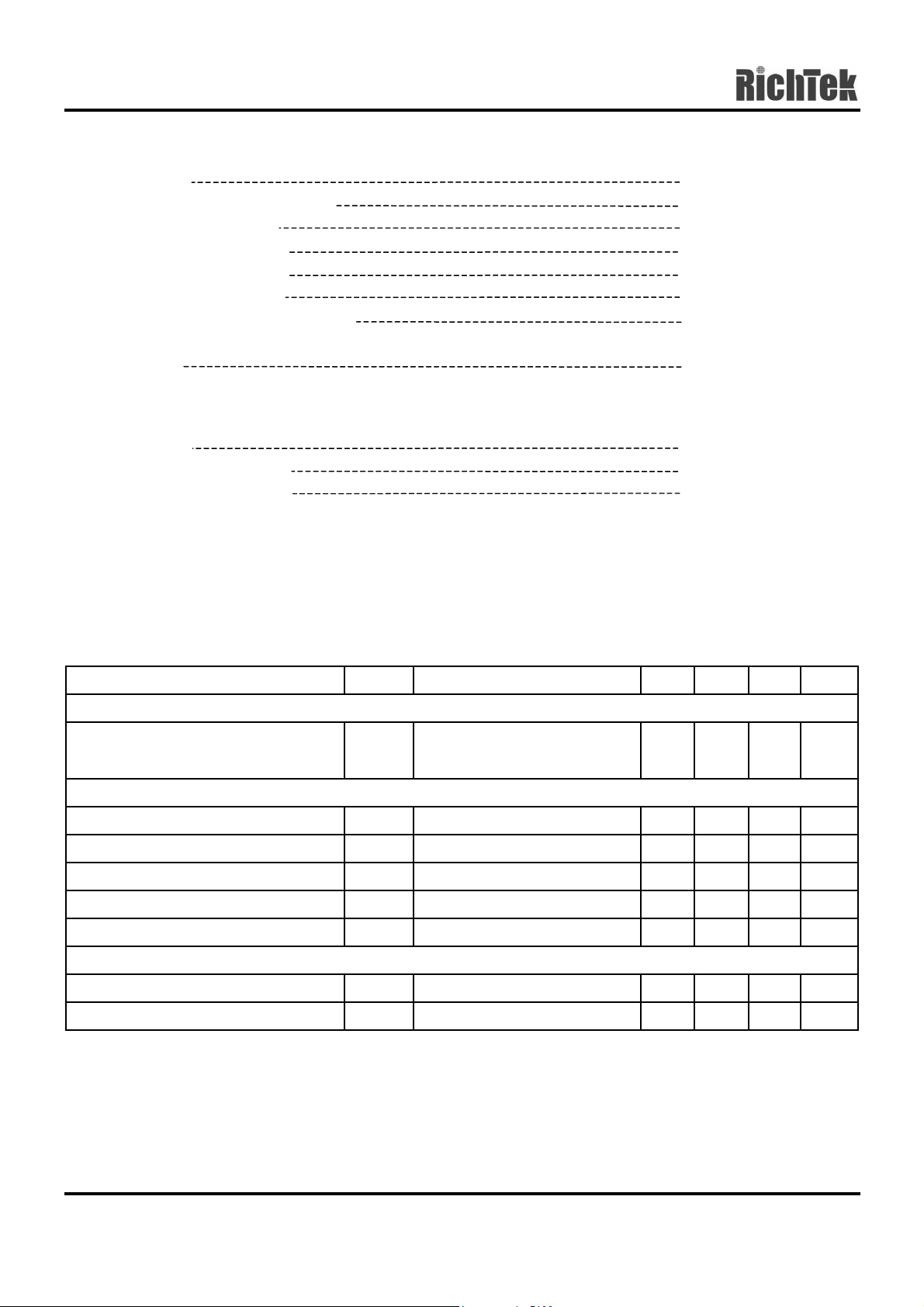
Supply Voltage +15V
z
PGOOD, FAULT and GATE Voltage GND−0.3V to VCC+0.3V
z
Input, Output or I/O Voltage GND−0.3V to 7V
z
Ambient Temperature Range 0°C to +70°C
z
Junction Temperature Range 0°C to +125°C
z
Storage Temperature Range −65°C to +150°C
z
Lead Temperature (Soldering, 10 sec.) 300°C
z
Package Thermal Resistance
SOP-28, θ
JA
Recommended Operating Conditions
z
Supply Voltage +12V ±10%
z
Ambient Temperature Range 0°C to 70°C
z
Junction Temperature Range 0°C to 125°C
CAUTION:
Stresses beyond the ratings specified in “Absolute Maximum Ratings” may cause permanent damage to the
device. This is a stress only rating and operation of the device at these or any other conditions above those
indicated in the operational sections of this specification is not implied.
60°C/W
Electrical Characteristics
(V
= 12V, PGND = 0V, TA = 25°C, unless otherwise specified)
CC
Parameter Symbol Test Conditions Min Typ Max Units
VCC Supply Current
Nominal Supply Current
I
CC
UGATE1, LGATE1, UGATE2,
DRIVE3, and DRIVE4 Open
Power-on Reset
VCC Rising Threshold
VCC Falling Threshold
Rising VAUX Threshold
VAUX Threshold Hysteresis
Rising V
OCSET1 (and 2)
Threshold
V
V
V
V
OCSET
OCSET
OCSET
OCSET
= 4.5V
= 4.5V
= 4.5V
= 4.5V
Oscillator
Free Running Frequency 180 200 225
Ramp Amplitude
∆V
OSC
-- 10 -- mA
7.5 -- 9.5 V
7--9V
-- 2.8 -- V
-- 0.5 --
-- 1.25 --
-- 1.9 --
To be continued
V
V
kHz
V
P-P
www.richtek-ic.com.tw DS9230-03 July 2001
2

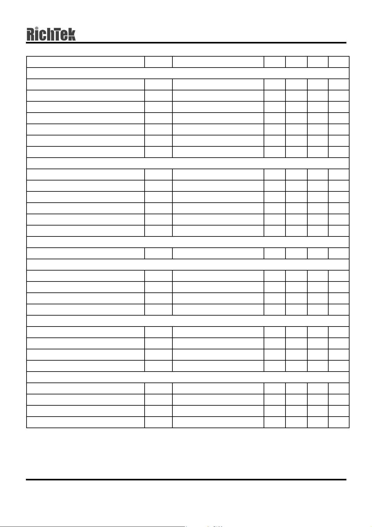
Parameter Symbol Test Conditions Min Typ Max Units
DAC and Standard Buck Regulator Reference
RT9230
DAC (VID0 ~ VID4) Input Low Voltage -- -- 0.8
DAC (VID0 ~ VID4) Input High Voltage 2 -- --
DACOUT Voltage Accuracy DACOUT = 2.05 ~ 3.50V -1 -- 1
DACOUT Voltage Accuracy DACOUT = 1.30 ~ 2.00V -1% -- 20mV
AGP PWM Reference Voltage
AGP PWM Reference Voltage
SELECT < 0.8V
SELECT > 2.0V
-- 1.5 --
-- 3.3 --
AGP PWM Reference Voltage Tolerance -2.5 -- 2.5
1.5V and 1.8V Linear Regulators (V
OUT3
and V
OUT4
)
Regulation -3 -- 3
VSEN3 Under-voltage Level VSEN3 Rising -- 1.125 --
VSEN3 Under-voltage Hysteresis VSEN3 Falling -- 100 --
VSEN4 Under-voltage Level VSEN4 Rising -- 1.350 --
VSEN4 Under-voltage Hysteresis VSEN4 Falling -- 100 --
Output Drive Current VAUX = 5V 20 40 --
Synchronous PWM Controller Error Amplifier
DC Gain -- 65 --
PWM Controller Gate Driver
V
V
%
--
V
V
%
%
V
mV
V
mV
mA
dB
UGATE 1 (and 2) Source
UGATE 1 (and 2) Sink
LGATE Source
LGATE Sink
R
UGATE
R
UGATEVUGATE
I
LGATE1
R
LGATE1VLGATE1
VCC = 12V, VCC-V
VCC = 12V, V
= 1V
= 1V
LGATE1
UGATE
= 2V
= 1V
-- 4 7
-- 3 7
-- 1 --
-- 2 6
Protection
VSEN1 Over-voltage (VSEN1/DACOUT) VSEN1 Rising 112 115 120
FAULT Sourcing Current
OCSET1, 2 Current Source
Soft-start Current
V
FAULT/RT
I
OCSETVOCSET
I
SS
= 2.0V
= 4.5V
10 14 --
170 200 230
-- 28 --
Power Good
V
Upper Threshold
OUT1
V
Under Voltage
OUT1
V
Hysteresis (VSEN1/DACOUT)
OUT1
PGOOD Voltage Low
V
PGOODIPGOOD
VSEN1 Rising 108 -- 112
VSEN1 Rising 87 -- 95
Upper/Lower Threshold -- 2 --
= -4mA
-- -- 0.5
Ω
Ω
A
Ω
%
mA
µA
µA
%
%
%
V
DS9230-03 July 2001 www.richtek-ic.com.tw
3
 Loading...