

RT9228
Advanced PWM and Dual Linear Power Controller
General Description
The RT9228 is a 3-in-one power controller optimized
for high-performance microprocessor and computer
applications. The IC integrates a synchronous buck
PWM controller, a linear regulator, and a linear
controller as well as monitoring and protection
functions into a 24-pin SOP package. The PWM
controller regulates the microprocessor core voltage.
The linear regulator provides power for the clock
driver circuit and the linear controller regulates power
for the GTL bus.
The RT9228 features an Intel-compatible, TTL 5-bit
programmable DAC that adjusts the core voltage
from 2.1V to 3.5V in 0.1V increments and from 1.3V
to 2.05V in 0.05V steps. The 5-bit DAC has a typical
±1% tolerance. The linear regulator uses an internal
drive device to provide 2.5V ±2.5% output voltage.
The linear controller drives an external N-channel
MOSFET or a low cost NPN bipolar transistor to
provide 1.5V ±2.5%.
Features
z
3-in-one Regulated Voltages for Microprocessor
Core, Clock, and GTL
z
Compatible with HIP6018B
z
Power-good Output Voltage Monitor
Switching section
z
5-bit DAC Programmable from 1.3V to 3.5V
±±±±1% DAC Accuracy
z
z
Fast Transient Response
z
Full 0% to 100% Duty Cycle Driver
z
Fixed 200kHz Switching Frequency
z
Adaptive Non-overlapping Gate Driver
z
Over-current Monitor Uses MOSFET R
z
Over-voltage Protection Uses Lower MOSFET
Linear Section
z
User-adjustable Linear Regulator Output Voltage
z
MOSFET or NPN Driving Capability
z
Ultra Fast Response Speed
z
Under-voltage Protection
z
Internal Thermal Shutdown
DS(ON)
The RT9228 monitors all the output voltages. A
Power-good signal is issued when the core voltage is
within ±10% of the DAC setting and the other levels
are above their under-voltage levels. Additional build-
in over-voltage protection for the core output uses
the lower MOSFET to prevent output voltage above
115% of the DAC setting. The PWM over-current
function monitors the output current using the voltage
drop across the upper MOSFET’s R
DS(ON)
, which
eliminates the need for a current sensing resistor.
Ordering Information
RT9228
Package type
S : SOP-24
Operating temperature range
C: Commercial standard
Applications
Full Motherboard Power Regulation for Computer
z
Low-voltage Distribution Power Supplies
z
Pin Configurations
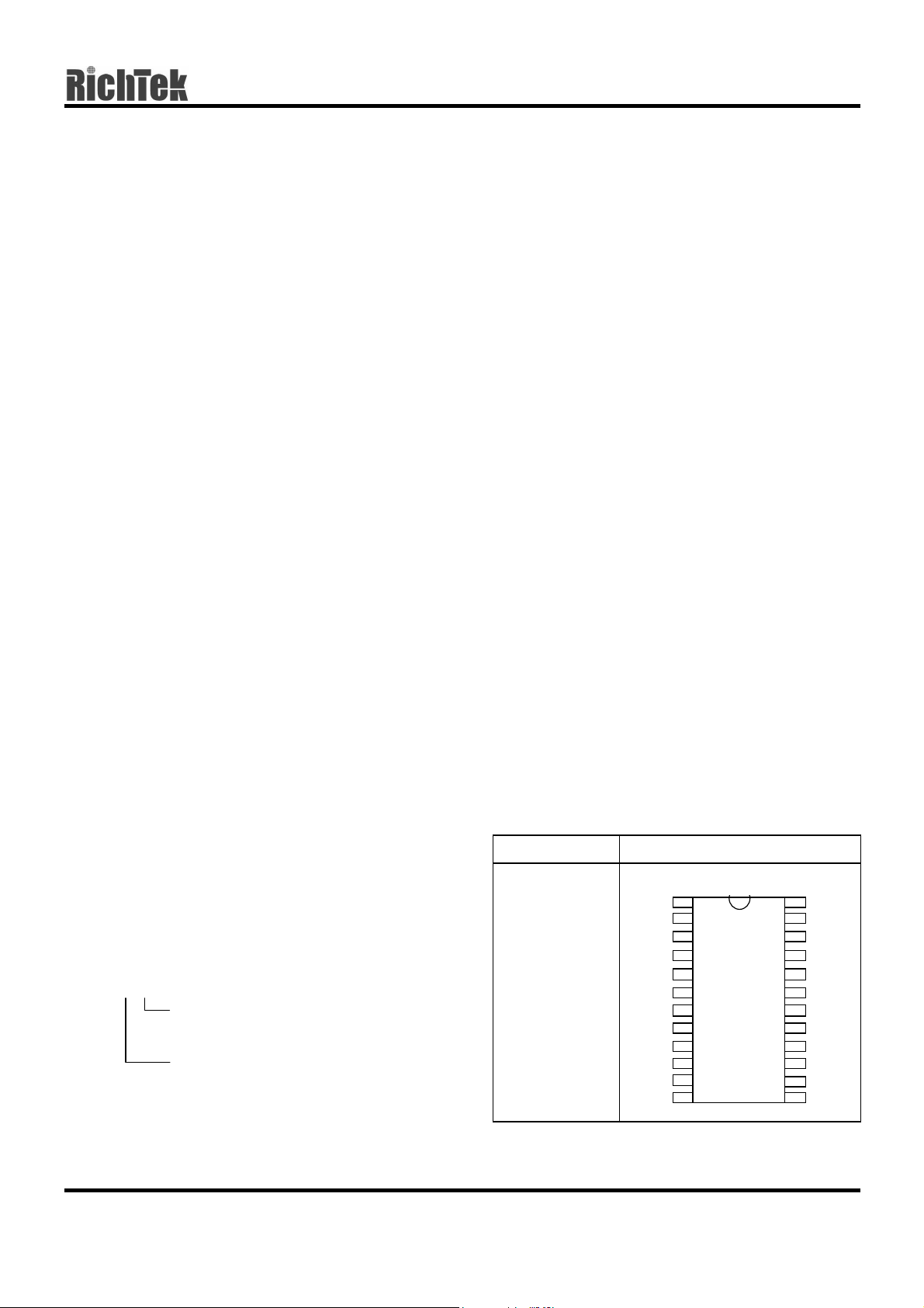
Part Number Pin Configurations
RT9228CS
(Plastic SOP-24)
VCC
VID4
VID3
VID2
VID1
VID0
PGOOD
FAULT
SS
NC
FB2 GND
VIN2
TOP VIEW
1
2
3
4
5
6
7
8
9
10
11
12 13
24
23
22
21
20
19
18
17
16
15
14
UGATE1
PHASE1
LGATE1
PGND
OCSET1
VSEN1
FB1
NC
FB3
GATE3
VOT2
DS9228-03 July 2001 www.richtek-ic.com.tw
1
RT9228
Absolute Maximum Ratings
z Supply Voltage +15V
z PGOOD, FAULT and GATE Voltage GND−0.3V to V
z Input, Output or I/O Voltage GND−0.3V to 7V
z Ambient Temperature Range 0°C to +70°C
z Junction Temperature Range 0°C to +125°C
z Storage Temperature Range −65°C to +150°C
z Lead Temperature (Soldering, 10 sec.) 300°C
z Package Thermal Resistance
SOP-24, θ
JA
Recommended Operating Conditions
z Supply Voltage +12V±10%
z Ambient Temperature Range 0°C to 70°C
z Junction Temperature Range 0°C to 125°C
CAUTION:
Stresses beyond the ratings specified in “Absolute Maximum Ratings” may cause permanent damage to the
device. This is a stress only rating and operation of the device at these or any other conditions above those
indicated in the operational sections of this specification is not implied.
75°C/W
CC
+0.3V
Electrical Characteristics
(V
= 12V, PGND = 0V, TA = 25°C, unless otherwise specified)
CC
Parameter Symbol Test Conditions Min Typ Max Units
VCC Supply Current
Nominal Supply Current
I
CC
Power-On Reset
VCC Rising Threshold
VCC Falling Threshold
Rising VIN2 Under-voltage Threshold -- 2.8 -- V
VIN2 Under-voltage Hysteresis -- 0.5 --
Rising V
OCSET1
Threshold
Oscillator
Free Running Frequency 180 200 225
Ramp Amplitude
∆V
OSC
UGATE1, GATE3, LGATE1,
and VOUT2 Open
V
OCSET1
V
OCSET1
= 4.5V
= 4.5V
-- 10 -- mA
7.5 -- 9.5 V
7--9V
-- 1.25 --
-- 1.9 --
To be continued
V
V
kHz
V
P-P
www.richtek-ic.com.tw DS9228-03 July 2001
2
Parameter Symbol Test Conditions Min Typ Max Units
Reference and DAC
RT9228
DAC (VID0-VID4) Input Low Voltage -- -- 0.8
DAC (VID0-VID4) Input High Voltage 2.0 -- --
DACOUT Voltage Accuracy DACOUT = 2.05 ~ 3.50V -1 -- 1
DACOUT Voltage Accuracy DACOUT = 1.30 ~ 2.00V -1% -- 20mV
Reference Voltage (Pin FB2 and FB3)
V
REF
1.240 1.265 1.290
Linear Regulator
Regulation
10mA < I
VOUT2
< 150mA
-2.5 -- 2.5
Under-voltage Level FB2 Rising -- 75 87
Under-voltage Hysteresis -- 100 --
Over-current Protection
I
OVP
180 230 --
Over-current Protection During Start-up -- 700 --
Linear Controller
Regulation
VSEN3 = GATE3
GATE3
< 20mA
0 < I
-2.5 -- 2.5
Under-voltage Level FB3 Rising -- 75 87
Under-voltage Hysteresis -- 100 --
Output Drive Current
VIN2 – VOUT3 > 1.5V
20 40 --
V
V
%
-
V
%
%
mV
mA
mA
%
%
mV
mA
PWM Controller Error Amplifier
DC Gain -- 65 --
PWM Controller Gate Driver
UGATE Source
UGATE Sink
LGATE Source
LGATE Sink
R
UGATE1
R
UGATE1VUGATE1
VCC - V
VCC = 12V
I
VCC = 12V
LGATE1
R
LGATE1VLGATE1
V
LGATE1
UGATE1
= 1V
= 2V
= 1V
= 1V
-- 3 7
-- 3 7
-- 1 --
-- 2 6
Protection
V
Over-voltage Trip
OUT1
FAULT Souring Current
OCSET1 Current Source
Soft-start Current
I
OVP
I
OCSET
I
SS
VSEN1 Rising 112 115 120
V
V
FAULT
OCSET1
= 8V
VSS = 1V
= 4.5V
10 14 --
170 200 230
-- 11 --
Power Good
V
Upper Threshold
OUT1
V
Under Voltage
OUT1
V
Hysteresis (VSEN1/DACOUT)
OUT1
PGOOD Voltage Low
V
PGOOD
VSEN1 Rising 108 -- 112
VSEN1 Rising 89 -- 95
Upper/Lower Threshold -- 2 --
I
PGOOD
= -4mA
-- -- 0.5
dB
Ω
Ω
A
Ω
%
mA
µA
µA
%
%
%
V
DS9228-03 July 2001 www.richtek-ic.com.tw
3
RT9228
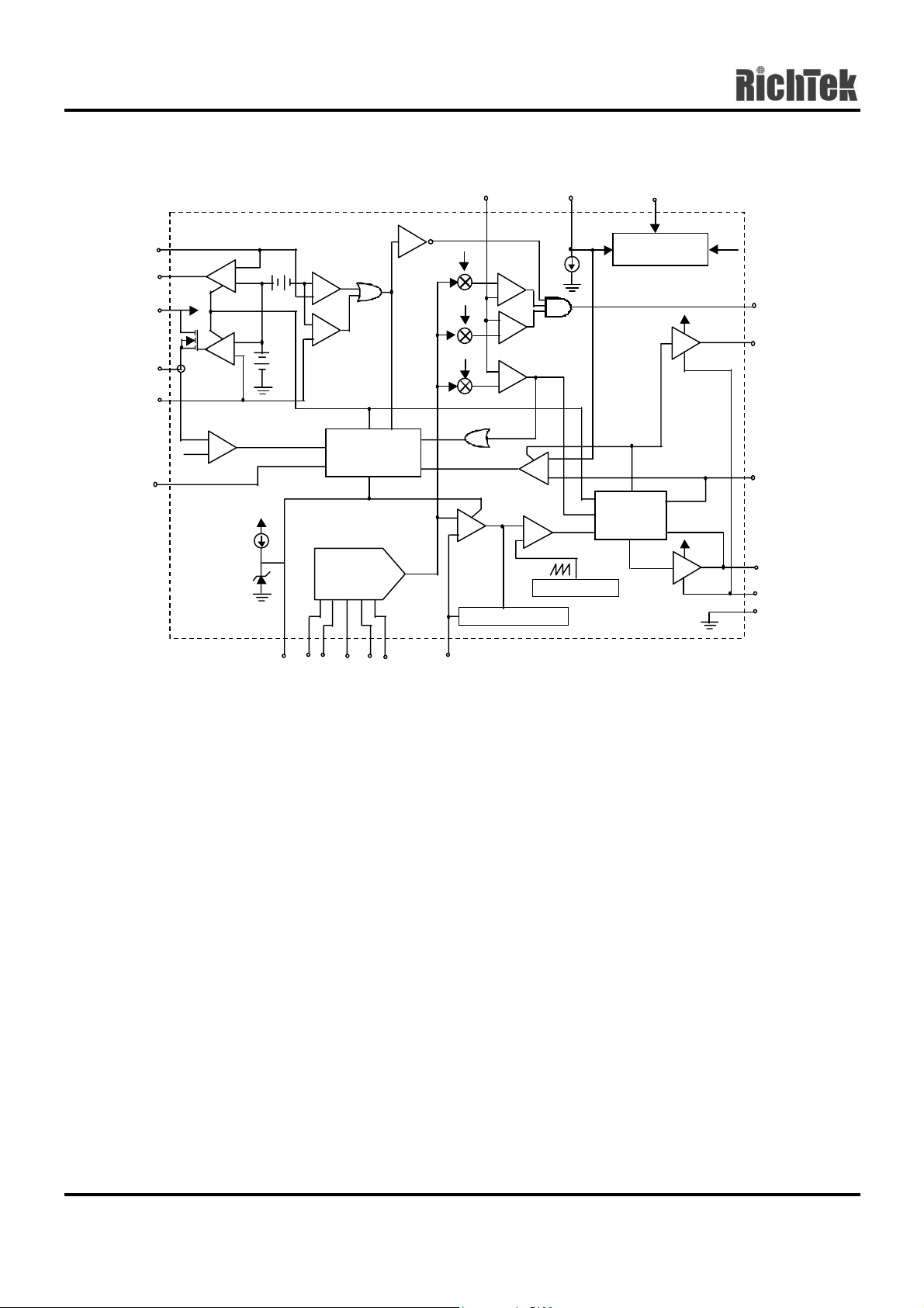
Function Block Diagram
FB3
GATE3
VIN2
VOUT2
FB2
FAULT
3.3V
0.25A
OCSET1VSEN1
+
_
+
_
+
_
OC1
+
_
OSCILLATOR
200µA
+
_
INHIBIT
PWM
PWM COMP
LINEAR
_
0.3V
+
1.26V
+
_
+
_
VCC
11µA
5V
UNDER
VOLTAGE
+
_
+
_
OC2
SOFT-START
& FAULT
LOGIC
DACO UT
TTL D/A
CONVERTER
(DAC)
110%
90%
115%
LUV
0V
+
_
ERRO R
AMP
COMPENSATION
VCC
POWER-ON
RESET (POR)
UPPER
DRIVE
GATE
CONTROL
LOGIC
LOWER
DRIVE
3.3V
PGOOD
VCC
UGATE1
PHASE1
VCC
LGATE1
PGND
GND
SS
VID1
VID4
VID3
VID2
VID0
Functional Pin Description
VCC (Pin 1)
Provide a 12V bias supply for the IC to this pin. This
pin also provides the gate bias charge for all the
MOSFETs controlled by the IC.
VID0, VID1, VID2, VID3, VID4 (Pin 6, 5, 4, 3, and 2)
VID0~4 are the input pins to the 5-bit DAC. The
states of these five pins program the internal voltage
reference, DACOUT. The level of DACOUT sets the
core converter output voltage. It also sets the core
PGOOD and OVP thresholds. Table 1 specifies the
DACOUT voltage of 32 combinations of VID levels.
PGOOD (Pin 7)
PGOOD is an open collector output used to indicate
the status of the output voltage. This pin is pulled low
when the core output is not within ±10% of the
FB1
DACOUT reference voltage and the other outputs are
below their under-voltage thresholds.
The PGOOD output is open for ‘11111’ VID codes
that inhibit operation. See table 1.
FAULT (Pin 8)
This pin is low during normal operation, but it is
pulled to about 8V (V
= 12V) in the event of an
CC
over-voltage or over-current condition.
SS (Pin 9)
Connect a capacitor from this pin to ground. This
capacitor, along with an internal 11µA (V
SS
>1V)
current source, sets the soft-start interval of the
converter.
www.richtek-ic.com.tw DS9228-03 July 2001
4

RT9228
FB2 (Pin 11)
Connect this pin to a resistor divider to set the linear
regulator output voltage. VIN2 (Pin 12) this pin
supplies power to the internal regulator. Connect this
pin to a suitable 3.3V source.
Additionally, this pin is used to monitor the 3.3V
supply. If, following a startup cycle, the voltage drops
below 2.8V (typically), the chip shuts down. A new
soft-start cycle is initiated upon return of the 3.3V
supply above the under-voltage threshold.
VOUT2 (Pin 13)
Output of the linear regulator. Supplies current up to
230mA.
GND (Pin 14)
Signal ground for the IC. All voltage levels are
measured with respect to this pin.
GATE3 (Pin 15)
Connect this pin to drive gate of an external
MOSFET or NPN. This pin provides the drive for the
linear controller’s pass transistor.
converter over-current (OC) trip point according to
the following equation:
I
PEAK
=
I
OCSET1
R
×R
DS (ON)
OCSET1
An over-current trip cycles the soft-start function.
Sustaining an over-current for 2 soft-start intervals
shuts down the controller.
PGND (Pin 21)
This is the power ground of UGATE1 and LGATE1.
Tie the PWM converter’s lower MOSFET source to
this pin.
LGATE1 (Pin 22)
Connect LGATE1 to the PWM converter’s lower
MOSFET gate. This pin provides the gate drive for
the lower MOSFET.
PHASE1 (Pin 23)
Connect the PHASE1 pin to the PWM converter’s
upper MOSFET source. This pin is used to monitor
the voltage drop across the upper MOSFET for over-
current protection.
FB3 (Pin 16)
Connect this pin to a resistor divider to set the linear
controller output voltage.
FB1 (Pin 18)
The FB1 pin is the inverting input of the error
amplifier.
VSEN1 (Pin 19)
This pin is connected to the PWM converter’s output
voltage. The PGOOD and OVP comparator circuits
use this signal to report output voltage status and for
over voltage protection.
OCSET1 (Pin 20)
Connect a resistor (R
OCSET1
drain of the upper MOSFET. R
200µA current source (I
MOSFET on-resistance (R
) from this pin to the
, an internal
OCSET
OCSET1
DS(ON)
), and the upper
) set the PWM
UGATE1 (Pin 24)
Connect UGATE1 pin to the PWM converter’s upper
MOSFET gate. This pin provides the gate drive for
the upper MOSFET.
DS9228-03 July 2001 www.richtek-ic.com.tw
5

RT9228
Table 1. VOUT1 Voltage Program
Pin Name
VID4 VID3 VID2 VID1 VID0
01111 1.30
01110 1.35
01101 1.40
01100 1.45
01011 1.50
01010 1.55
01001 1.60
01000 1.65
00111 1.70
00110 1.75
00101 1.80
00100 1.85
00011 1.90
00010 1.95
00001 2.00
Normal OUT1 Voltage
DACOUT
00000 2.05
11111 INHIBIT
11110 2.10
11101 2.20
11100 2.30
11011 2.40
11010 2.50
11001 2.60
11000 2.70
10111 2.80
10110 2.90
10101 3.00
10100 3.10
10011 3.30
10010 3.30
10001 3.40
10000 3.50
www.richtek-ic.com.tw DS9228-03 July 2001
6
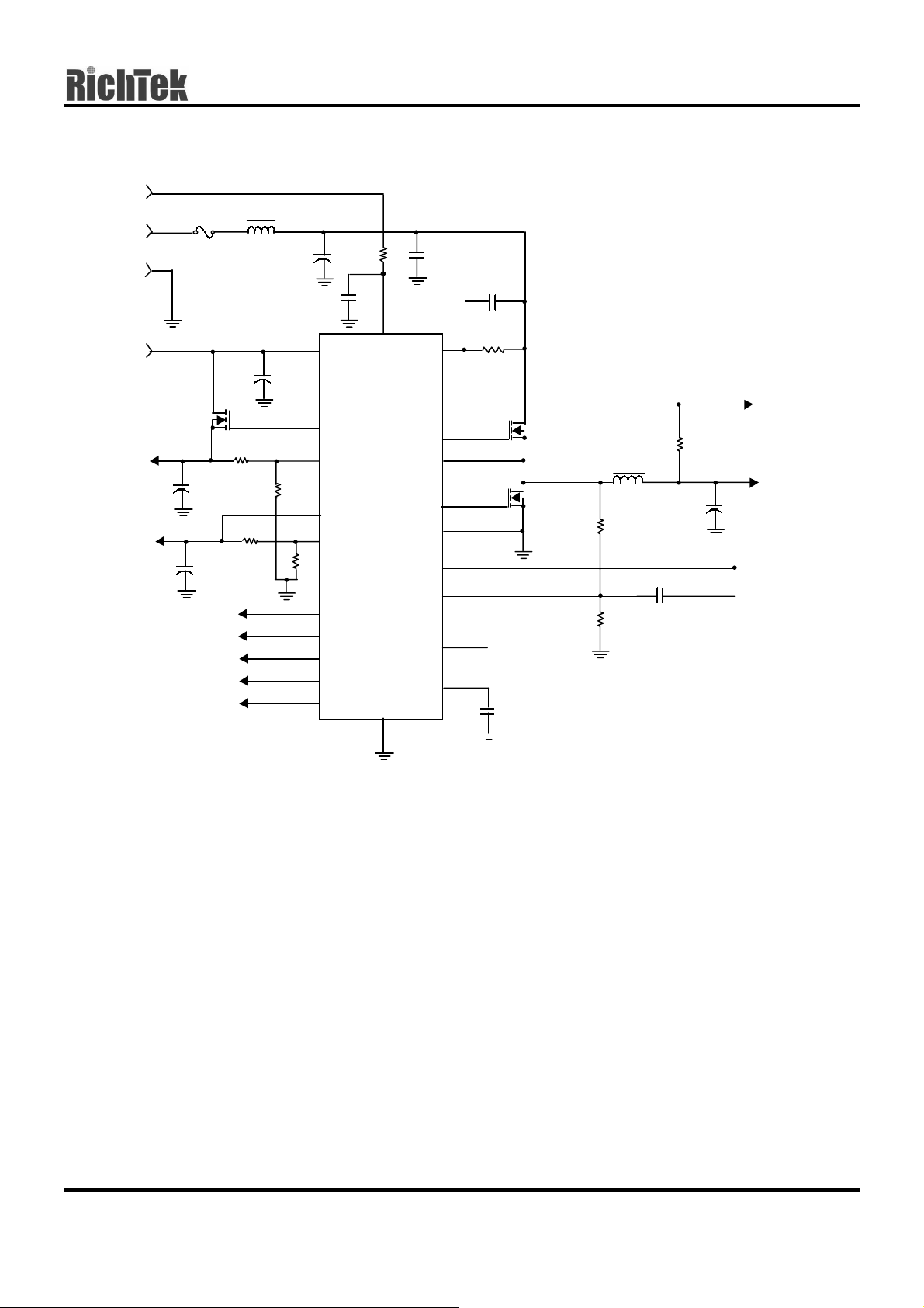
Typical Application Circuit
12V
L1
1µH
4x1000µF
R6
187
R8
1K
C1-4
+
C8
1000µF
R7
1K
12
15
16
13
11
R9
1K
5
4
3
2
6
+
GATE3
FB3
FB2
VID0
5V
GND
3.3V
V
OUT3
1.5V
V
OUT2
2.5V
Q3
RFD3055
+
+
F1
15A
C9
1000µF
C10
270µF
C20
1µF
VIN2
RT9228
VOUT2
VID1
VID2
VID3
VID4
R1
10
1
VCC
OCSET1
OCSET1
PGOOD
UGATE1
PHASE1
LGATE1
GND
14
PGND
VSEN1
FB1
FAULT
SS
C5-6
2x1µF
20
7
24
23
22
21
19
18
8
9
C7
1000pF
R2
1.21k
C12
0.039µF
Q1
PHB83N03LT
PHB95N03LT
Q2
L2
3.5µH
R4
4.99K
R5
732K
POWERGOOD
R3
10K
C13-1 9
7x1000µF
C11
0.68µF
RT9228
V
OUT1
1.3 to 3.5V
+
DS9228-03 July 2001 www.richtek-ic.com.tw
7

RT9228
Package Information
H
M
B
A
C
FD
Dimensions In Millimeters Dimensions In Inches
Symbol
Min Max Min Max
A 15.189 15.596 0.598 0.614
B 7.391 7.595 0.291 0.299
C 2.362 2.642 0.093 0.104
D 0.330 0.508 0.013 0.020
I
B
J
F 1.194 1.346 0.047 0.053
H 0.229 0.330 0.009 0.013
I 0.102 0.305 0.004 0.012
J 10.008 10.643 0.394 0.419
M 0.381 1.270
www.richtek-ic.com.tw DS9228-03 July 2001
0.015 0.050
8

RT9228
DS9228-03 July 2001 www.richtek-ic.com.tw
9

RT9228
RICHTEK TECHNOLOGY CORP.
Headquarter
6F, No. 35, Hsintai Road, Chupei City
Hsinchu, Taiwan, R.O.C.
Tel: (8863)5510047 Fax: (8863)5537749
www.richtek-ic.com.tw DS9228-03 July 2001
RICHTEK TECHNOLOGY CORP.
Taipei Office (Marketing)
8F-1, No. 137, Lane 235, Paochiao Road, Hsintien City
Taipei County, Taiwan, R.O.C.
Tel: (8862)89191466 Fax: (8862)89191465
Email: marketing@richtek-ic.com.tw
10
 Loading...